EP0935292A2 - Method of manufacturing a MOSFET - Google Patents
Method of manufacturing a MOSFET Download PDFInfo
- Publication number
- EP0935292A2 EP0935292A2 EP99107808A EP99107808A EP0935292A2 EP 0935292 A2 EP0935292 A2 EP 0935292A2 EP 99107808 A EP99107808 A EP 99107808A EP 99107808 A EP99107808 A EP 99107808A EP 0935292 A2 EP0935292 A2 EP 0935292A2
- Authority
- EP
- European Patent Office
- Prior art keywords
- film
- semiconductor layer
- germanium
- insulating film
- silicon
- Prior art date
- Legal status (The legal status is an assumption and is not a legal conclusion. Google has not performed a legal analysis and makes no representation as to the accuracy of the status listed.)
- Ceased
Links
- 238000004519 manufacturing process Methods 0.000 title description 11
- 239000004065 semiconductor Substances 0.000 claims abstract description 69
- 230000001590 oxidative effect Effects 0.000 claims abstract description 8
- 229910020751 SixGe1-x Inorganic materials 0.000 claims description 9
- 239000010408 film Substances 0.000 abstract description 125
- 239000000758 substrate Substances 0.000 abstract description 47
- 239000010409 thin film Substances 0.000 abstract description 37
- 229910052732 germanium Inorganic materials 0.000 abstract description 22
- GNPVGFCGXDBREM-UHFFFAOYSA-N germanium atom Chemical compound [Ge] GNPVGFCGXDBREM-UHFFFAOYSA-N 0.000 abstract description 22
- 229910052710 silicon Inorganic materials 0.000 abstract description 12
- 239000010703 silicon Substances 0.000 abstract description 12
- 230000003647 oxidation Effects 0.000 description 29
- 238000007254 oxidation reaction Methods 0.000 description 29
- 239000011521 glass Substances 0.000 description 28
- 238000000034 method Methods 0.000 description 28
- VYPSYNLAJGMNEJ-UHFFFAOYSA-N silicon dioxide Inorganic materials O=[Si]=O VYPSYNLAJGMNEJ-UHFFFAOYSA-N 0.000 description 27
- 229910000577 Silicon-germanium Inorganic materials 0.000 description 25
- LEVVHYCKPQWKOP-UHFFFAOYSA-N [Si].[Ge] Chemical compound [Si].[Ge] LEVVHYCKPQWKOP-UHFFFAOYSA-N 0.000 description 22
- 229910021420 polycrystalline silicon Inorganic materials 0.000 description 15
- 229910052681 coesite Inorganic materials 0.000 description 12
- 229910052906 cristobalite Inorganic materials 0.000 description 12
- 239000000377 silicon dioxide Substances 0.000 description 12
- 229910052682 stishovite Inorganic materials 0.000 description 12
- 229910052905 tridymite Inorganic materials 0.000 description 12
- XUIMIQQOPSSXEZ-UHFFFAOYSA-N Silicon Chemical compound [Si] XUIMIQQOPSSXEZ-UHFFFAOYSA-N 0.000 description 11
- 230000005587 bubbling Effects 0.000 description 11
- PZPGRFITIJYNEJ-UHFFFAOYSA-N disilane Chemical compound [SiH3][SiH3] PZPGRFITIJYNEJ-UHFFFAOYSA-N 0.000 description 10
- 239000007789 gas Substances 0.000 description 10
- 238000005229 chemical vapour deposition Methods 0.000 description 9
- 239000012535 impurity Substances 0.000 description 9
- 150000002500 ions Chemical class 0.000 description 9
- 230000008569 process Effects 0.000 description 9
- IJGRMHOSHXDMSA-UHFFFAOYSA-N Atomic nitrogen Chemical compound N#N IJGRMHOSHXDMSA-UHFFFAOYSA-N 0.000 description 8
- 238000005530 etching Methods 0.000 description 8
- 229910000078 germane Inorganic materials 0.000 description 8
- 238000010438 heat treatment Methods 0.000 description 7
- 239000000463 material Substances 0.000 description 7
- 239000011651 chromium Substances 0.000 description 6
- 238000000206 photolithography Methods 0.000 description 6
- XLYOFNOQVPJJNP-UHFFFAOYSA-N water Substances O XLYOFNOQVPJJNP-UHFFFAOYSA-N 0.000 description 6
- 229910052581 Si3N4 Inorganic materials 0.000 description 4
- 229910052782 aluminium Inorganic materials 0.000 description 4
- XAGFODPZIPBFFR-UHFFFAOYSA-N aluminium Chemical compound [Al] XAGFODPZIPBFFR-UHFFFAOYSA-N 0.000 description 4
- QVGXLLKOCUKJST-UHFFFAOYSA-N atomic oxygen Chemical compound [O] QVGXLLKOCUKJST-UHFFFAOYSA-N 0.000 description 4
- 238000000151 deposition Methods 0.000 description 4
- 238000009792 diffusion process Methods 0.000 description 4
- QUZPNFFHZPRKJD-UHFFFAOYSA-N germane Chemical compound [GeH4] QUZPNFFHZPRKJD-UHFFFAOYSA-N 0.000 description 4
- 229910052986 germanium hydride Inorganic materials 0.000 description 4
- 239000004973 liquid crystal related substance Substances 0.000 description 4
- 229910052757 nitrogen Inorganic materials 0.000 description 4
- 239000001301 oxygen Substances 0.000 description 4
- 229910052760 oxygen Inorganic materials 0.000 description 4
- 229910007264 Si2H6 Inorganic materials 0.000 description 3
- 239000000370 acceptor Substances 0.000 description 3
- 229910045601 alloy Inorganic materials 0.000 description 3
- 239000000956 alloy Substances 0.000 description 3
- 229910021417 amorphous silicon Inorganic materials 0.000 description 3
- 238000001505 atmospheric-pressure chemical vapour deposition Methods 0.000 description 3
- 229910052796 boron Inorganic materials 0.000 description 3
- 238000004140 cleaning Methods 0.000 description 3
- 239000013078 crystal Substances 0.000 description 3
- 238000002425 crystallisation Methods 0.000 description 3
- 230000008025 crystallization Effects 0.000 description 3
- 239000010453 quartz Substances 0.000 description 3
- HQVNEWCFYHHQES-UHFFFAOYSA-N silicon nitride Chemical compound N12[Si]34N5[Si]62N3[Si]51N64 HQVNEWCFYHHQES-UHFFFAOYSA-N 0.000 description 3
- 125000006850 spacer group Chemical group 0.000 description 3
- ZOXJGFHDIHLPTG-UHFFFAOYSA-N Boron Chemical compound [B] ZOXJGFHDIHLPTG-UHFFFAOYSA-N 0.000 description 2
- VYZAMTAEIAYCRO-UHFFFAOYSA-N Chromium Chemical compound [Cr] VYZAMTAEIAYCRO-UHFFFAOYSA-N 0.000 description 2
- KRHYYFGTRYWZRS-UHFFFAOYSA-N Fluorane Chemical compound F KRHYYFGTRYWZRS-UHFFFAOYSA-N 0.000 description 2
- 229910004205 SiNX Inorganic materials 0.000 description 2
- BLRPTPMANUNPDV-UHFFFAOYSA-N Silane Chemical compound [SiH4] BLRPTPMANUNPDV-UHFFFAOYSA-N 0.000 description 2
- -1 aluminum (Al) Chemical class 0.000 description 2
- 229910052804 chromium Inorganic materials 0.000 description 2
- 229910021419 crystalline silicon Inorganic materials 0.000 description 2
- 230000007423 decrease Effects 0.000 description 2
- 230000008021 deposition Effects 0.000 description 2
- 239000001257 hydrogen Substances 0.000 description 2
- 229910052739 hydrogen Inorganic materials 0.000 description 2
- 238000005984 hydrogenation reaction Methods 0.000 description 2
- 238000002513 implantation Methods 0.000 description 2
- 238000001465 metallisation Methods 0.000 description 2
- 238000000926 separation method Methods 0.000 description 2
- 238000004544 sputter deposition Methods 0.000 description 2
- 229910052715 tantalum Inorganic materials 0.000 description 2
- GUVRBAGPIYLISA-UHFFFAOYSA-N tantalum atom Chemical compound [Ta] GUVRBAGPIYLISA-UHFFFAOYSA-N 0.000 description 2
- 239000010936 titanium Substances 0.000 description 2
- UFHFLCQGNIYNRP-UHFFFAOYSA-N Hydrogen Chemical compound [H][H] UFHFLCQGNIYNRP-UHFFFAOYSA-N 0.000 description 1
- ZOKXTWBITQBERF-UHFFFAOYSA-N Molybdenum Chemical compound [Mo] ZOKXTWBITQBERF-UHFFFAOYSA-N 0.000 description 1
- GRYLNZFGIOXLOG-UHFFFAOYSA-N Nitric acid Chemical compound O[N+]([O-])=O GRYLNZFGIOXLOG-UHFFFAOYSA-N 0.000 description 1
- 229910003070 TaOx Inorganic materials 0.000 description 1
- RTAQQCXQSZGOHL-UHFFFAOYSA-N Titanium Chemical compound [Ti] RTAQQCXQSZGOHL-UHFFFAOYSA-N 0.000 description 1
- OQNXPQOQCWVVHP-UHFFFAOYSA-N [Si].O=[Ge] Chemical compound [Si].O=[Ge] OQNXPQOQCWVVHP-UHFFFAOYSA-N 0.000 description 1
- 238000000137 annealing Methods 0.000 description 1
- 229910052785 arsenic Inorganic materials 0.000 description 1
- RQNWIZPPADIBDY-UHFFFAOYSA-N arsenic atom Chemical compound [As] RQNWIZPPADIBDY-UHFFFAOYSA-N 0.000 description 1
- 230000015572 biosynthetic process Effects 0.000 description 1
- 229910052799 carbon Inorganic materials 0.000 description 1
- 239000000969 carrier Substances 0.000 description 1
- 230000008859 change Effects 0.000 description 1
- 238000001312 dry etching Methods 0.000 description 1
- 230000000694 effects Effects 0.000 description 1
- 230000005684 electric field Effects 0.000 description 1
- 239000007772 electrode material Substances 0.000 description 1
- 230000002708 enhancing effect Effects 0.000 description 1
- 230000005669 field effect Effects 0.000 description 1
- BHEPBYXIRTUNPN-UHFFFAOYSA-N hydridophosphorus(.) (triplet) Chemical compound [PH] BHEPBYXIRTUNPN-UHFFFAOYSA-N 0.000 description 1
- 150000002431 hydrogen Chemical class 0.000 description 1
- 125000004435 hydrogen atom Chemical group [H]* 0.000 description 1
- 230000006872 improvement Effects 0.000 description 1
- 239000011261 inert gas Substances 0.000 description 1
- 238000009413 insulation Methods 0.000 description 1
- 239000012212 insulator Substances 0.000 description 1
- 229910052751 metal Inorganic materials 0.000 description 1
- 239000002184 metal Substances 0.000 description 1
- 150000002739 metals Chemical class 0.000 description 1
- 239000000203 mixture Substances 0.000 description 1
- 230000004048 modification Effects 0.000 description 1
- 238000012986 modification Methods 0.000 description 1
- 229910052750 molybdenum Inorganic materials 0.000 description 1
- 239000011733 molybdenum Substances 0.000 description 1
- 229910017604 nitric acid Inorganic materials 0.000 description 1
- 230000003071 parasitic effect Effects 0.000 description 1
- 238000000059 patterning Methods 0.000 description 1
- 230000001698 pyrogenic effect Effects 0.000 description 1
- 230000009467 reduction Effects 0.000 description 1
- 229910000077 silane Inorganic materials 0.000 description 1
- 239000007787 solid Substances 0.000 description 1
- 239000007790 solid phase Substances 0.000 description 1
- 229910052719 titanium Inorganic materials 0.000 description 1
Images


Classifications
-
- H—ELECTRICITY
- H01—ELECTRIC ELEMENTS
- H01L—SEMICONDUCTOR DEVICES NOT COVERED BY CLASS H10
- H01L29/00—Semiconductor devices adapted for rectifying, amplifying, oscillating or switching, or capacitors or resistors with at least one potential-jump barrier or surface barrier, e.g. PN junction depletion layer or carrier concentration layer; Details of semiconductor bodies or of electrodes thereof ; Multistep manufacturing processes therefor
- H01L29/66—Types of semiconductor device ; Multistep manufacturing processes therefor
- H01L29/66007—Multistep manufacturing processes
- H01L29/66075—Multistep manufacturing processes of devices having semiconductor bodies comprising group 14 or group 13/15 materials
- H01L29/66227—Multistep manufacturing processes of devices having semiconductor bodies comprising group 14 or group 13/15 materials the devices being controllable only by the electric current supplied or the electric potential applied, to an electrode which does not carry the current to be rectified, amplified or switched, e.g. three-terminal devices
- H01L29/66409—Unipolar field-effect transistors
- H01L29/66477—Unipolar field-effect transistors with an insulated gate, i.e. MISFET
- H01L29/66568—Lateral single gate silicon transistors
- H01L29/66575—Lateral single gate silicon transistors where the source and drain or source and drain extensions are self-aligned to the sides of the gate
- H01L29/6659—Lateral single gate silicon transistors where the source and drain or source and drain extensions are self-aligned to the sides of the gate with both lightly doped source and drain extensions and source and drain self-aligned to the sides of the gate, e.g. lightly doped drain [LDD] MOSFET, double diffused drain [DDD] MOSFET
-
- H—ELECTRICITY
- H01—ELECTRIC ELEMENTS
- H01L—SEMICONDUCTOR DEVICES NOT COVERED BY CLASS H10
- H01L21/00—Processes or apparatus adapted for the manufacture or treatment of semiconductor or solid state devices or of parts thereof
- H01L21/02—Manufacture or treatment of semiconductor devices or of parts thereof
- H01L21/04—Manufacture or treatment of semiconductor devices or of parts thereof the devices having at least one potential-jump barrier or surface barrier, e.g. PN junction, depletion layer or carrier concentration layer
- H01L21/18—Manufacture or treatment of semiconductor devices or of parts thereof the devices having at least one potential-jump barrier or surface barrier, e.g. PN junction, depletion layer or carrier concentration layer the devices having semiconductor bodies comprising elements of Group IV of the Periodic System or AIIIBV compounds with or without impurities, e.g. doping materials
- H01L21/28—Manufacture of electrodes on semiconductor bodies using processes or apparatus not provided for in groups H01L21/20 - H01L21/268
- H01L21/28008—Making conductor-insulator-semiconductor electrodes
- H01L21/28017—Making conductor-insulator-semiconductor electrodes the insulator being formed after the semiconductor body, the semiconductor being silicon
- H01L21/28026—Making conductor-insulator-semiconductor electrodes the insulator being formed after the semiconductor body, the semiconductor being silicon characterised by the conductor
- H01L21/2807—Making conductor-insulator-semiconductor electrodes the insulator being formed after the semiconductor body, the semiconductor being silicon characterised by the conductor the final conductor layer next to the insulator being Si or Ge or C and their alloys except Si
-
- H—ELECTRICITY
- H01—ELECTRIC ELEMENTS
- H01L—SEMICONDUCTOR DEVICES NOT COVERED BY CLASS H10
- H01L29/00—Semiconductor devices adapted for rectifying, amplifying, oscillating or switching, or capacitors or resistors with at least one potential-jump barrier or surface barrier, e.g. PN junction depletion layer or carrier concentration layer; Details of semiconductor bodies or of electrodes thereof ; Multistep manufacturing processes therefor
- H01L29/40—Electrodes ; Multistep manufacturing processes therefor
- H01L29/43—Electrodes ; Multistep manufacturing processes therefor characterised by the materials of which they are formed
- H01L29/49—Metal-insulator-semiconductor electrodes, e.g. gates of MOSFET
- H01L29/4908—Metal-insulator-semiconductor electrodes, e.g. gates of MOSFET for thin film semiconductor, e.g. gate of TFT
-
- H—ELECTRICITY
- H01—ELECTRIC ELEMENTS
- H01L—SEMICONDUCTOR DEVICES NOT COVERED BY CLASS H10
- H01L29/00—Semiconductor devices adapted for rectifying, amplifying, oscillating or switching, or capacitors or resistors with at least one potential-jump barrier or surface barrier, e.g. PN junction depletion layer or carrier concentration layer; Details of semiconductor bodies or of electrodes thereof ; Multistep manufacturing processes therefor
- H01L29/66—Types of semiconductor device ; Multistep manufacturing processes therefor
- H01L29/66007—Multistep manufacturing processes
- H01L29/66075—Multistep manufacturing processes of devices having semiconductor bodies comprising group 14 or group 13/15 materials
- H01L29/66227—Multistep manufacturing processes of devices having semiconductor bodies comprising group 14 or group 13/15 materials the devices being controllable only by the electric current supplied or the electric potential applied, to an electrode which does not carry the current to be rectified, amplified or switched, e.g. three-terminal devices
- H01L29/66409—Unipolar field-effect transistors
- H01L29/66477—Unipolar field-effect transistors with an insulated gate, i.e. MISFET
- H01L29/66742—Thin film unipolar transistors
-
- H—ELECTRICITY
- H01—ELECTRIC ELEMENTS
- H01L—SEMICONDUCTOR DEVICES NOT COVERED BY CLASS H10
- H01L29/00—Semiconductor devices adapted for rectifying, amplifying, oscillating or switching, or capacitors or resistors with at least one potential-jump barrier or surface barrier, e.g. PN junction depletion layer or carrier concentration layer; Details of semiconductor bodies or of electrodes thereof ; Multistep manufacturing processes therefor
- H01L29/66—Types of semiconductor device ; Multistep manufacturing processes therefor
- H01L29/68—Types of semiconductor device ; Multistep manufacturing processes therefor controllable by only the electric current supplied, or only the electric potential applied, to an electrode which does not carry the current to be rectified, amplified or switched
- H01L29/76—Unipolar devices, e.g. field effect transistors
- H01L29/772—Field effect transistors
- H01L29/78—Field effect transistors with field effect produced by an insulated gate
- H01L29/786—Thin film transistors, i.e. transistors with a channel being at least partly a thin film
- H01L29/78684—Thin film transistors, i.e. transistors with a channel being at least partly a thin film having a semiconductor body comprising semiconductor materials of Group IV not being silicon, or alloys including an element of the group IV, e.g. Ge, SiN alloys, SiC alloys
-
- H—ELECTRICITY
- H01—ELECTRIC ELEMENTS
- H01L—SEMICONDUCTOR DEVICES NOT COVERED BY CLASS H10
- H01L2924/00—Indexing scheme for arrangements or methods for connecting or disconnecting semiconductor or solid-state bodies as covered by H01L24/00
- H01L2924/0001—Technical content checked by a classifier
- H01L2924/0002—Not covered by any one of groups H01L24/00, H01L24/00 and H01L2224/00
Definitions
- the present invention relates to a thin film semiconductor device, and a method for fabricating such a thin film semiconductor device.
- the present invention relates to a thin film semiconductor device used for a liquid crystal display device (hereinafter, abbreviated as "LCD") for driving liquid crystal, a sensor for reading images, a load of RAM (Random Access Memory) and the like, and a method for fabricating such a thin film semiconductor device.
- LCD liquid crystal display device
- RAM Random Access Memory
- a thin film semiconductor device includes a thin film semiconductor layer formed on a substrate having an insulating surface such as a quartz substrate or a glass substrate.
- a thin film transistor (TFT) is utilized in various fields.
- TFT thin film transistor
- a conventional example of a polycrystalline silicon thin film transistor, which has been developed for the use for a liquid crystal display (LCD) will be described.
- a polycrystalline silicon thin film transistor (hereinafter, referred to as a "low-temperature poly-Si TFT"), which can be fabricated at a relatively low temperature (about 600°C or less) at which inexpensive glass substrates can be used instead of expensive quartz substrates, has attracted attention.
- a relatively low temperature about 600°C or less
- one of the important problems to be solved of the low-temperature poly-Si TFT is the improvement in quality of a gate insulating film. Therefore, various gate insulating films have been examined.
- the low-temperature poly Si TFT is fabricated as follows.
- an amorphous silicon film is deposited on a top surface of a substrate 12 , and then it is irradiated with a laser light so as to locally heat and melt the amorphous silicon film. As a result, the amorphous silicon film is crystallized, thereby obtaining a polycrystalline silicon film 13 . Thereafter, the polycrystalline silicon film 13 is patterned into an island shape by photolithography and etching ( Figure 4A ).
- a gate insulating film 14 which consists of an SiO 2 layer is formed on the polycrystalline silicon film 13 by using an ECR-CVD method ( Figure 4B )
- a gate electrode 15 made of tantalum (Ta) is formed on the gate insulating film 14 .
- impurities serving as donors or acceptors are introduced into the polycrystalline silicon film 13 by ion doping in which mass separation is not conducted, thereby forming a source region 16 and a drain region 17 ( Figure 4C ).
- a source electrode 19 and a drain electrode 20 are formed on the insulating film 18 .
- a low-temperature poly-Si TFT shown in Figure 4D is fabricated.
- the gate insulating film 14 which consists of an SiO 2 film is deposited by the ECR-CVD (Electron Cyclotron Resonance Chemical Vapor Deposition) method. Therefore, it has been reported that the low-temperature poly-Si TFT has good characteristics as compared with SiO 2 deposited by an AP-CVD (Atmospheric Pressure Chemical Vapor Deposition) method or LTO (low temperature oxide).
- AP-CVD atmospheric Pressure Chemical Vapor Deposition
- LTO low temperature oxide
- the reason for this is that the SiO 2 layer functioning as the gate insulating film 14 is deposited after the polycrystalline silicon layer 13 is formed and the substrate is subjected to processes such as a cleaning process.
- the state of the interface between the insulating film deposited by a CVD method and the semiconductor may greatly change due to various conditions such as a cleaning condition before depositing the insulating film, waiting time after the cleaning until deposition, an atmosphere immediately before the deposition.
- the interfacial states at the semiconductor/insulating film interface may be remarkably degraded.
- characteristics of a thin film transistor are prone to be degraded.
- this method is not suitable for mass production.
- the method has another problem that the production yield is low due to pin holes of the insulating film and the like since the gate insulating film is obtained by a CVD method.
- a thermal oxide film made of silicon is generally utilized as a gate insulating film in order that the interfacial states density is controlled at a predetermined level or a lower level.
- growth of such a thermal oxide film requires high temperature process. Therefore, it is necessary to use an expensive quartz substrate which induces no strain even in a high-temperature process, resulting in an increase in the fabrication cost.
- the semiconductor device includes a semiconductor layer made of Si x Ge 1-x (0 ⁇ x ⁇ 1) and an insulating film formed on the semiconductor layer, wherein the insulating film includes an Si x Ge 1-x O 2 thermal oxide film formed by thermally oxidizing a surface of the semiconductor layer.
- the semiconductor layer functions as an interconnection line.
- the semiconductor layer functions as a gate electrode.
- a glass substrate (glass #1737, fabricated by Corning Inc.) 1 on which an SiO 2 film acting as a buffer layer (not shown) is deposited in order to prevent the diffusion of impurities from the glass substrate, is used.
- the glass substrate 1 has a strain point of 667°C. From the viewpoint of reduction in cost, it is preferable to use an inexpensive glass having a strain point as low as possible as the glass substrate 1 . Considering expansion or warp of the glass substrate 1 due to heat, it is preferable that the strain point of the glass substrate 1 is about +50°C or more of the process maximum temperature.
- an amorphous silicon-germanium film containing germanium at a concentration of 25% (hereinafter, referred to as an "a-Si 0.75 Ge 0.25 " film) is grown on the glass substrate 1 to a thickness of 100 nm.
- the a-Si 0.75 Ge 0.25 film is formed by a CVD method using, for example, disilane (Si 2 H 6 ) and germane (GeH 4 ) as material gases.
- the flow rate of disilane is in the range of 20 to 50 sccm
- the flow rate of germane is 10 to 30 sccm. It goes without saying that the flow rate of the gas changes depending on the size of the chamber and the like.
- the temperature of the glass substrate 1 during growth of the film is set to be in the range of 450°C to 600°C.
- the a-Si 0.75 Ge 0.25 film is patterned to form an island region having the size in accordance with the size of a transistor to be formed.
- the size of one island region is, for example, 10 ⁇ m ⁇ 50 ⁇ m.
- FIG 1A only one island region is shown. In actual, however, a plurality of island regions can be simultaneously formed.
- the patterning of the a-Si 0.75 Ge 0.25 film can be carried out using normal photolithography and etching.
- an etchant for example, a mixture of hydrofluoric acid and nitric acid and the like can be used. In the case where dry etching is conducted, CF 4 or SF 6 to which O 2 is added is used.
- an excimer laser light having a wavelength of 308 nm is radiated onto the a-Si 0.75 Ge 0.25 film so as to melt/solidify (crystallize) the a-Si 0.75 Ge 0.25 film.
- a semiconductor layer 2 made of polycrystalline silicon-germanium hereinafter, referred to as "poly-Si 0.75 Ge 0.25 " is obtained. While the a-Si 0.75 Ge 0.25 film is crystallized after being patterned in Example 1, the a-Si 0.75 Ge 0.25 film may be crystallized before being patterned.
- a preferred thickness of the thermal oxide film is in the range of 50 nm to 200 nm.
- pyrogenic oxidation or dry oxidation may be used instead of steam oxidation.
- an oxidation method using the steam obtained by bubbling is suitable for obtaining a thermal oxide film having good quality at a relatively low temperature, for example, at about 600°C or lower.
- the oxidation temperature is preferably 700°C or lower, more preferably, 600°C or lower.
- a chromium (Cr) film having a thickness of about 200 nm is deposited onto the gate insulating film 3 by, for example, sputtering, the Cr film is patterned by photolithography and etching, thereby forming a gate electrode 4 as shown in Figure 1C .
- impurity ions 5 acting as donors or acceptors are implanted into the semiconductor layer 2 .
- the impurity implantation is conducted by ion doping in which mass separation is not performed (alternatively, by bucket type ion doping method described in, for example, Extended Abstracts of the 22nd (1990) International Conference on Solid State Devices and Materials, p. 971 or p.1197).
- Plasma doping may be used instead of ion doping. Thereafter, a heat treatment (annealing) is conducted at a temperature in the range of about 300°C to 600°C so as to activate the impurities implanted into the semiconductor layer 2 , thereby forming a source region 6 and a drain region 6 as shown in Figure 1C .
- annealing is conducted at a temperature in the range of about 300°C to 600°C so as to activate the impurities implanted into the semiconductor layer 2 , thereby forming a source region 6 and a drain region 6 as shown in Figure 1C .
- an interlevel insulating film 8 which consists of an SiO 2 film by an Atmospheric-Pressure CVD method
- contact holes are formed in the interlevel insulating film 8 .
- a conductive film such as an aluminum (Al) film is formed on the interlevel insulating film 8 by sputtering.
- the conductive film is patterned by photolithography and etching so as to form a source electrode 9 and a drain electrode 10 , thereby forming a thin film transistor as shown in Figure 1D .
- the semiconductor layer 2 is made of silicon-germanium alloy
- the gate insulating film 3 is made of the thermal oxide film obtained by thermally oxidizing the surface of the semiconductor layer 2 . With this process, a cleaned interface of semiconductor/insulating film is formed. Therefore, a thin film transistor having excellent performance and high reliability can be fabricated. Furthermore, since the thin film transistor can be fabricated at a relatively low temperature, i.e., 600°C or lower, not only a low-cost glass substrate can be used, but also the production yield can be enhanced.
- the hydrogenation process is carried out by exposing the substrate to hydrogen plasma or hydrogen atoms at a substrate temperature of about 300°C, at any stage from the formation step of the source region 6 and the drain region 7 to the completion of the thin film transistor.
- the semiconductor layer of the present invention is not limited to the concentration.
- the oxidation temperature is about 600°C
- the oxidation rate is increased as the germanium concentration increases.
- the oxidation time period is shortened. Therefore, it is preferable that the semiconductor layer 2 is made of Si x Ge 1-x (0 ⁇ x ⁇ 0.8).
- the germanium concentration is high. According to the present invention, a thin film transistor having the electron mobility of 50 cm 2 /V ⁇ sec or more and the hole mobility of 30 cm 2 /V ⁇ sec or more can be obtained.
- Example 1 a polycrystalline silicon-germanium layer, which is subjected to a crystallization process using a laser light, is used as the semiconductor layer 2 .
- a single-crystalline silicon-germanium layer, which is epitaxially grown on a single-crystalline semiconductor substrate, or a single-crystalline silicongermanium layer having an SOI (Semiconductor On Insulator) structure may also be used.
- Cr is used as a material of the gate electrode 4 and Al is used as a material of the source electrode 9 and the drain electrode 10 in Example 1, metals such as aluminum (Al), tantalum (Ta), molybdenum (Mo), chromium (Cr) and titanium (Ti), and alloys thereof may be used as electrode materials.
- metals such as aluminum (Al), tantalum (Ta), molybdenum (Mo), chromium (Cr) and titanium (Ti), and alloys thereof may be used as electrode materials.
- heavily doped polycrystalline silicon, a polycrystalline silicon-germanium alloy, or transparent conductive layers such as ITO may also be used.
- LDD lightly doped drain
- N-channel type transistor by selectively using, as impurities, boron, arsenic and the like acting as acceptors and phosphorous, aluminum and the like acting as donors.
- a CMOS circuit is integrated on the substrate.
- a glass substrate for example, glass #1733, fabricated by Corning Inc. 1 , on which an SiO 2 film acting as a buffer layer (not shown) is deposited in order to prevent the diffusion of impurities from the glass substrate, is used.
- an amorphous silicon-germanium film containing germanium at a concentration of 50% (hereinafter, referred to as an "a-Si 0.50 Ge 0.50 " film) is formed on the glass substrate 1 to a thickness of 100 nm.
- the a-Si 0.50 Ge 0.50 film is formed by CVD method using, for example, disilane (Si 2 H 6 ) and germane (GeH 4 ) as material gases.
- the flow rate of disilane is in the range of 20 to 50 sccm
- the flow rate of germane is 20 to 50 sccm. It goes without saying that the flow rate of the gas changes depending on the size of the chamber and the like.
- the temperature of the glass substrate 1 during growth of the film is set to be in the range of 450°C to 600°C.
- a heat treatment is conducted at, for example, 550°C, thereby obtaining a semiconductor layer 2a made of polycrystalline silicon-germanium (hereinafter, referred to as "poly-Si 0.50 Ge 0.50 ").
- This heat treatment can be conducted by using a conventional electric furnace in a vacuum atmosphere or an inert gas atmosphere.
- the glass substrate 1 is inserted into a furnace at 550°C. Pure water held at 95°C is subjected to bubbling with nitrogen or gaseous oxygen. By using steam obtained by the bubbling, the surface of the semiconductor layer 2a is thermally oxidized for two hours in the furnace. By the thermal oxidation, a thermal oxide film having a thickness of about 100 nm is formed. The thus obtained thermal oxide film, which is made of Si 0.50 Ge 0.50 O 2 , is used as a gate insulating film 3 .
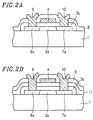
- a gate electrode 4 , a source region 6a , a drain region 7a , an insulating film 8 , a source electrode 9 and a drain electrode 10 are formed in the same manner as that of Example 1, thereby obtaining a thin film transistor shown in Figure 2A .
- the polycrystalline silicon-germanium layer which is crystallized by heat treatment, is used as the semiconductor layer 2a , a single-crystalline silicon-germanium layer may also be used. Moreover, the polycrystalline silicon-germanium layer, which is crystallized by laser irradiation, may also be used.
- the gate insulating film 3 is formed by thermally oxidizing the semiconductor layer 2 containing germanium at a concentration of 25% at 600°C for two hours in Example 1, and is formed by thermally oxidizing the semiconductor layer 2a containing germanium at a concentration of 50% at 550°C for two hours in Example 2.
- the oxidation temperature of Example 2 is lower than that of Example 1. When the oxidation temperature is low, the oxidation rate also decreases. However, the decrease in the oxidation rate is compensated by enhancing the germanium concentration, thereby holding the same oxidation time period.
- a glass substrate for example, glass #1733, fabricated by Corning Inc. 1 , on which an SiO 2 film acting as a buffer layer (not shown) is deposited in order to prevent the diffusion of an impurity from the glass substrate, is used.
- the thin film transistor of Example 3 differs from those described in the preceding examples in that the thin film transistor of Example 3 has a gate insulating film having a double-layered structure. More specifically, a second gate insulating film 11 which consists of a silicon nitride (SiN x ) layer is formed on a first gate insulating film 3a (Si 0.50 Ge 0.50 O 2 ) serving as a thermal oxide film.
- a second gate insulating film 11 which consists of a silicon nitride (SiN x ) layer is formed on a first gate insulating film 3a (Si 0.50 Ge 0.50 O 2 ) serving as a thermal oxide film.
- an amorphous silicon-germanium film containing germanium at a concentration of 50% (hereinafter, referred to as an "a-Si 0.50 Ge 0.50 " film) is formed on the glass substrate 1 to a thickness of 100 nm.
- the a-Si 0.50 Ge 0.50 film is formed by a CVD method using, for example, disilane (Si 2 H 6 ) and germane (GeH 4 ) as material gases.
- the flow rate of disilane is in the range of 20 to 50 sccm
- the flow rate of germane is 20 to 50 sccm. It goes without saying that the flow rate of the gas changes depending on the size of the chamber and the like.
- the temperature of the glass substrate 1 during growth of the film is set to be in the range of 450°C to 600°C.
- the a-Si 0.50 Ge 0.50 film is patterned to form an island region having the size in accordance with the size of a transistor element to be formed.
- FIG 2B only one island region is shown. In actual, however, a plurality of island regions may be simultaneously formed.
- the a-Si 0.50 Ge 0.50 thin film can be carried out using the same photolithography and etching as those of the preceding examples.
- a heat treatment is conducted at, for example, 550°C, thereby obtaining a semiconductor layer 2 made of polycrystalline silicon-germanium (hereinafter, referred to as "poly-Si 0.50 Ge 0.50 ").
- the glass substrate 1 is inserted into a furnace at 550°C. Pure water held at 95°C is subjected to bubbling with nitrogen or gaseous oxygen. By using steam obtained by the bubbling, the surface of the semiconductor layer 2 is thermally oxidized for two hours in the furnace. By the thermal oxidation, a thermal oxide film having a thickness of about 100 nm is formed.
- the thus obtained thermal oxide film which is made of Si 0.50 Ge 0.50 O 2 , is used as a first gate insulating film 3a .
- the thickness of the thermal oxide film changes depending on the conditions such as the concentration of germanium in silicon-germanium, the substrate temperature, the temperature of pure water serving as a steam source, the flow rate of bubbling gas, and oxidation time period.
- a silicon nitride (SiN x ) layer is formed to a thickness of 100 nm by a CVD method, thereby obtaining the second insulating film 11 .
- the same steps as those of Examples 1 and 2 are carried out, thereby forming the thin film transistor shown in Figure 2B.
- the insulation properties of the gate insulating films are improved, and therefore, the production yield is further improved.
- the thermal oxide film (first gate insulating film) can be thinned.
- a time period required for thermal oxidation can be reduced.
- the thermal oxidation time may be shortened to about an hour. If the oxidation time is shortened, the processing throughput is improved.
- a silicon nitride film is used as the second gate insulating film 11 in Example 3, other insulating films such as an SiO 2 film, a TaO x film may also be used.
- the semiconductor layer 2a can also be obtained by crystallization with laser irradiation. Moreover, a single-crystalline silicon-germanium layer may also be used as the semiconductor layer 2a .
- the germanium concentration is preferably 20% or higher in terms of mobility.
- carriers electron or holes
- the germanium concentration is high.
- the crystal grain size cannot be formed so large.
- the semiconductor layer 2 or 2a is formed by laser irradiation, although the crystallization can be advantageously performed at room temperature, the crystal grain size cannot be formed so large.
- the semiconductor layer 2 or 2a is formed by heat treatment, although a relatively high temperature (about 550°C) is required, the crystal grain has a large size, i.e., about one to several tens ⁇ m. As the crystal grain size becomes large, the mobility is further improved.
- any substrate can be used as long as it has an insulating surface.
- a normal single-crystalline silicon substrate whose upper surface is covered with an insulating film, may also be used.
- a device in which a transistor formed on the single-crystalline silicon substrate and the thin film semiconductor device according to the present invention are integrated on the same substrate, is provided.
- the Si x Ge 1-x layer is used as an active layer of the thin film transistor and the Si x Ge 1-x O 2 thermal oxide film is used as a gate insulating film is described.
- the Si x Ge 1-x layer is also possible to use the Si x Ge 1-x layer as a conductive part of the gate electrode or the wiring in the semiconductor device, and the Si x Ge 1-x O 2 thermal oxide film as an insulating covering part of the conductive part. In such a case, appropriate impurities are doped into the semiconductor layer.
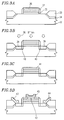
- a field oxide film 33 with an n + -channel stopper 34 is formed on an n - -type silicon substrate 32 by a LOCOS (Local Oxidation Of Silicon) method so as to surround an active region on which an MOS transistor is to be formed.
- a gate oxide film 35 is formed by thermal oxidation to a thickness of 10 to 30 nm.
- a polycrystalline silicon-germanium film is deposited to a thickness of 300 nm by using, for example, silane (SiH 4 ) and germane (GeH 4 ) as material gases.
- the flow rate of disilane is in the range of 20 to 50 sccm
- the flow rate of germane is 20 to 50 sccm. It goes without saying that the flow rate of the gas changes depending on the size of the chamber and the like.
- the temperature of the silicon substrate 32 during growth of the film is set to be in the range of 600°C to 650°C.
- gate oxide film 35 is selectively removed by etching using a gate electrode as a mask.
- sidewall spacers 37 are formed by etching back the SiO 2 film ( Figure 3A ).
- boron (B) ions 38 are implanted into the substrate 32 to form a p + -region (source/drain region) 39 by using the gate electrode and the spacer as masks ( Figure 3B ).
- the dose of ions is reduced below the spacers 37 to form p - -regions 40 .
- an LDD Lightly Doped Drain
- the silicon substrate 32 is inserted into a furnace at 600°C. Pure water held at 95°C is subjected to bubbling with nitrogen or gaseous oxygen. By using steam obtained by the bubbling, the surface of the polycrystalline silicon-germanium film layer is thermally oxidized for two hours in the furnace. By the thermal oxidation, a silicon-germanium oxide film 41 is formed ( Figure 3C ). Silicon is hardly oxidized at the oxidation temperature. Only the polycrystalline silicon-germanium serving as the gate electrode is selectively oxidized. As a result, the gate electrode is electrically isolated without forming the interlevel insulating layer.
- the through hole 42 is formed and the metallization for forming source/drain regions is conducted immediately after the polycrystalline silicongermanium film is oxidized, the following process is also applicable. After the polycrystalline silicon-germanium film is oxidized, an insulating layer made of SiO 2 and Si 3 N 4 is deposited by a CVD method. Thereafter, a through hole is formed. In this way, the production yield is further improved.
- Example 4 The method for forming the p-channel MOS transistor alone is described in Example 4. However, an n-channel MOS transistor or a CMOS structure can be produced by the same method. Furthermore, the method is also applicable to semiconductor devices other than the MOS transistor.
- the layer containing silicon and germanium is used as a gate electrode or a wiring, since the surface of the electrode or the wiring is covered with a thermal oxide film of high quality, the electrode or the wiring, which is hardly short-circuited, can be obtained.
Abstract
Description
- The present invention relates to a thin film semiconductor device, and a method for fabricating such a thin film semiconductor device. In particular, the present invention relates to a thin film semiconductor device used for a liquid crystal display device (hereinafter, abbreviated as "LCD") for driving liquid crystal, a sensor for reading images, a load of RAM (Random Access Memory) and the like, and a method for fabricating such a thin film semiconductor device.
- A thin film semiconductor device includes a thin film semiconductor layer formed on a substrate having an insulating surface such as a quartz substrate or a glass substrate. A thin film transistor (TFT) is utilized in various fields. Hereinafter, a conventional example of a polycrystalline silicon thin film transistor, which has been developed for the use for a liquid crystal display (LCD), will be described.
- Recently, in the field of the liquid crystal display using the thin film transistor, a polycrystalline silicon thin film transistor (hereinafter, referred to as a "low-temperature poly-Si TFT"), which can be fabricated at a relatively low temperature (about 600°C or less) at which inexpensive glass substrates can be used instead of expensive quartz substrates, has attracted attention. However, one of the important problems to be solved of the low-temperature poly-Si TFT is the improvement in quality of a gate insulating film. Therefore, various gate insulating films have been examined.
- A low-temperature poly-Si TFT described in "Society of Information Display International symposium Digest of Technical Papers / Volume XXIV (1993) pp. 387 - 390" will be briefly described as a conventional example, with reference to Figures 4A to 4D.
- The low-temperature poly Si TFT is fabricated as follows.
- First, an amorphous silicon film is deposited on a top surface of a
substrate 12, and then it is irradiated with a laser light so as to locally heat and melt the amorphous silicon film. As a result, the amorphous silicon film is crystallized, thereby obtaining apolycrystalline silicon film 13. Thereafter, thepolycrystalline silicon film 13 is patterned into an island shape by photolithography and etching (Figure 4A). - Next, after a
gate insulating film 14 which consists of an SiO2 layer is formed on thepolycrystalline silicon film 13 by using an ECR-CVD method (Figure 4B), agate electrode 15 made of tantalum (Ta) is formed on thegate insulating film 14. Thereafter, by using thegate electrode 15 as a mask, impurities serving as donors or acceptors are introduced into thepolycrystalline silicon film 13 by ion doping in which mass separation is not conducted, thereby forming asource region 16 and a drain region 17 (Figure 4C). After forming an interlevelinsulating film 18, asource electrode 19 and adrain electrode 20 are formed on theinsulating film 18. As a result, a low-temperature poly-Si TFT shown in Figure 4D is fabricated. - In the conventional low-temperature poly-Si TFT shown in Figures 4A to 4D, the
gate insulating film 14 which consists of an SiO2 film is deposited by the ECR-CVD (Electron Cyclotron Resonance Chemical Vapor Deposition) method. Therefore, it has been reported that the low-temperature poly-Si TFT has good characteristics as compared with SiO2 deposited by an AP-CVD (Atmospheric Pressure Chemical Vapor Deposition) method or LTO (low temperature oxide). However, even if the ECR-CVD method is used, the most important interface of semiconductor/insulating film, which affects device characteristics, becomes remarkably unstable. The reason for this is that the SiO2 layer functioning as thegate insulating film 14 is deposited after thepolycrystalline silicon layer 13 is formed and the substrate is subjected to processes such as a cleaning process. The state of the interface between the insulating film deposited by a CVD method and the semiconductor may greatly change due to various conditions such as a cleaning condition before depositing the insulating film, waiting time after the cleaning until deposition, an atmosphere immediately before the deposition. As a result, the interfacial states at the semiconductor/insulating film interface may be remarkably degraded. Thus, characteristics of a thin film transistor are prone to be degraded. Moreover, in order to perfectly control the interfacial states density, it is necessary to strictly control the fabrication conditions. Therefore, this method is not suitable for mass production. Furthermore, the method has another problem that the production yield is low due to pin holes of the insulating film and the like since the gate insulating film is obtained by a CVD method. - In the field of LSI, a thermal oxide film made of silicon is generally utilized as a gate insulating film in order that the interfacial states density is controlled at a predetermined level or a lower level. However, growth of such a thermal oxide film requires high temperature process. Therefore, it is necessary to use an expensive quartz substrate which induces no strain even in a high-temperature process, resulting in an increase in the fabrication cost.
- According to the present invention, the semiconductor device includes a semiconductor layer made of SixGe1-x (0 < x < 1) and an insulating film formed on the semiconductor layer, wherein the insulating film includes an SixGe1-xO2 thermal oxide film formed by thermally oxidizing a surface of the semiconductor layer.
- In one embodiment of the invention, the semiconductor layer functions as an interconnection line.
- In another embodiment of the invention, the semiconductor layer functions as a gate electrode.
- The advantages of the present invention will become apparent to those skilled in the art upon reading and understanding the following detailed description with reference to the accompanying figures.
-
- Figures 1A to 1D are schematic cross-sectional views each showing a main step of a fabrication method of a thin film transistor according to the present invention.
- Figure 2A is a schematic cross-sectional view showing another thin film transistor according to the present invention.
- Figure 2B is a schematic cross-sectional view showing still another thin film transistor according to the present invention.
- Figures 3A to 3D are schematic cross-sectional view showing still another thin film transistor according to the present invention.
- Figures 4A to 4D are schematic cross-sectional views each showing a main step of a fabrication method of a conventional thin film transistor.
-
- Hereinafter, the present invention will be described by way of illustrative examples with reference to the drawings.
- With reference to Figures 1A to 1D, a first example of a thin film semiconductor device according to the present invention will be described. In this example, a glass substrate (glass #1737, fabricated by Corning Inc.) 1, on which an SiO2 film acting as a buffer layer (not shown) is deposited in order to prevent the diffusion of impurities from the glass substrate, is used. The
glass substrate 1 has a strain point of 667°C. From the viewpoint of reduction in cost, it is preferable to use an inexpensive glass having a strain point as low as possible as theglass substrate 1. Considering expansion or warp of theglass substrate 1 due to heat, it is preferable that the strain point of theglass substrate 1 is about +50°C or more of the process maximum temperature. - First, an amorphous silicon-germanium film containing germanium at a concentration of 25% (hereinafter, referred to as an "a-Si0.75Ge0.25" film) is grown on the
glass substrate 1 to a thickness of 100 nm. The a-Si0.75Ge0.25 film is formed by a CVD method using, for example, disilane (Si2H6) and germane (GeH4) as material gases. Typically, the flow rate of disilane is in the range of 20 to 50 sccm, and the flow rate of germane is 10 to 30 sccm. It goes without saying that the flow rate of the gas changes depending on the size of the chamber and the like. It is preferable that the temperature of theglass substrate 1 during growth of the film is set to be in the range of 450°C to 600°C. - Next, the a-Si0.75Ge0.25 film is patterned to form an island region having the size in accordance with the size of a transistor to be formed. The size of one island region is, for example, 10 µm × 50 µm. In Figure 1A, only one island region is shown. In actual, however, a plurality of island regions can be simultaneously formed. The patterning of the a-Si0.75Ge0.25 film can be carried out using normal photolithography and etching. As an etchant, for example, a mixture of hydrofluoric acid and nitric acid and the like can be used. In the case where dry etching is conducted, CF4 or SF6 to which O2 is added is used.
- Thereafter, an excimer laser light having a wavelength of 308 nm is radiated onto the a-Si0.75Ge0.25 film so as to melt/solidify (crystallize) the a-Si0.75Ge0.25 film. In this way, a
semiconductor layer 2 made of polycrystalline silicon-germanium (hereinafter, referred to as "poly-Si0.75Ge0.25") is obtained. While the a-Si0.75Ge0.25 film is crystallized after being patterned in Example 1, the a-Si0.75Ge0.25 film may be crystallized before being patterned. - Next, the
glass substrate 1 is inserted into a furnace at 600°C. Pure water held at 95°C is subjected to bubbling with nitrogen or gaseous oxygen. By using steam obtained by the bubbling, the surface of thesemiconductor layer 2 is thermally oxidized for two hours in the furnace. By the thermal oxidation, as shown in Figure 1B, a thermal oxide film having a thickness of about 100 nm is formed. The thus obtained thermal oxide film, which is made of Si0.75Ge0.25O2, is used as agate insulating film 3. The thickness of the thermal oxide film changes depending on the conditions such as the concentration of germanium in silicon-germanium, the substrate temperature, the temperature of pure water serving as a steam source, the flow rate of bubbling gas and oxidation time period. In the case where the thermal oxide film is used as the gate insulating film of the thin film transistor, a preferred thickness of the thermal oxide film is in the range of 50 nm to 200 nm. As a method for thermally oxidizing the surface of thesemiconductor layer 2, pyrogenic oxidation or dry oxidation may be used instead of steam oxidation. However, an oxidation method using the steam obtained by bubbling is suitable for obtaining a thermal oxide film having good quality at a relatively low temperature, for example, at about 600°C or lower. - When silicon-germanium is thermally oxidized at about 700°C or higher, silicon is selectively oxidized rather than germanium. As a result, germanium is precipitated at the interface of semiconductor/insulating film or part containing a large amount of silicon and part containing a large amount of germanium are formed in a layered manner in the oxide film. Therefore, it is necessary to determine an oxidation temperature with care. The oxidation temperature is preferably 700°C or lower, more preferably, 600°C or lower.
- Next, after a chromium (Cr) film having a thickness of about 200 nm is deposited onto the
gate insulating film 3 by, for example, sputtering, the Cr film is patterned by photolithography and etching, thereby forming agate electrode 4 as shown in Figure 1C. Next, by using thegate electrode 4 as an implantation mask, impurity ions 5 acting as donors or acceptors are implanted into thesemiconductor layer 2. The impurity implantation is conducted by ion doping in which mass separation is not performed (alternatively, by bucket type ion doping method described in, for example, Extended Abstracts of the 22nd (1990) International Conference on Solid State Devices and Materials, p. 971 or p.1197). Plasma doping may be used instead of ion doping. Thereafter, a heat treatment (annealing) is conducted at a temperature in the range of about 300°C to 600°C so as to activate the impurities implanted into thesemiconductor layer 2, thereby forming asource region 6 and adrain region 6 as shown in Figure 1C. - Next, after forming an interlevel
insulating film 8 which consists of an SiO2 film by an Atmospheric-Pressure CVD method, contact holes are formed in the interlevelinsulating film 8. Thereafter, a conductive film such as an aluminum (Al) film is formed on the interlevelinsulating film 8 by sputtering. The conductive film is patterned by photolithography and etching so as to form asource electrode 9 and adrain electrode 10, thereby forming a thin film transistor as shown in Figure 1D. - In the thin film transistor of the present invention, the
semiconductor layer 2 is made of silicon-germanium alloy, and thegate insulating film 3 is made of the thermal oxide film obtained by thermally oxidizing the surface of thesemiconductor layer 2. With this process, a cleaned interface of semiconductor/insulating film is formed. Therefore, a thin film transistor having excellent performance and high reliability can be fabricated. Furthermore, since the thin film transistor can be fabricated at a relatively low temperature, i.e., 600°C or lower, not only a low-cost glass substrate can be used, but also the production yield can be enhanced. - If dangling bonds, which are present at the grain boundaries of a polycrystalline film, are terminated by hydrogen, transistor characteristics are further improved. Therefore, it is desirable to perform a hydrogenation process. The hydrogenation process is carried out by exposing the substrate to hydrogen plasma or hydrogen atoms at a substrate temperature of about 300°C, at any stage from the formation step of the
source region 6 and thedrain region 7 to the completion of the thin film transistor. - Moreover, although the silicon-germanium film having a germanium concentration of 25% is used as the
semiconductor layer 2 in Example 1, the semiconductor layer of the present invention is not limited to the concentration. Generally, in the case where the oxidation temperature is about 600°C, the oxidation rate is increased as the germanium concentration increases. As a result, the oxidation time period is shortened. Therefore, it is preferable that thesemiconductor layer 2 is made of SixGe1-x (0 < x < 0.8). Furthermore, since a field-effect mobility is increased as the germanium concentration increases, it is desirable that the germanium concentration is high. According to the present invention, a thin film transistor having the electron mobility of 50 cm2/V·sec or more and the hole mobility of 30 cm2/V·sec or more can be obtained. - In Example 1, a polycrystalline silicon-germanium layer, which is subjected to a crystallization process using a laser light, is used as the
semiconductor layer 2. A single-crystalline silicon-germanium layer, which is epitaxially grown on a single-crystalline semiconductor substrate, or a single-crystalline silicongermanium layer having an SOI (Semiconductor On Insulator) structure may also be used. - Although Cr is used as a material of the
gate electrode 4 and Al is used as a material of thesource electrode 9 and thedrain electrode 10 in Example 1, metals such as aluminum (Al), tantalum (Ta), molybdenum (Mo), chromium (Cr) and titanium (Ti), and alloys thereof may be used as electrode materials. Alternatively, heavily doped polycrystalline silicon, a polycrystalline silicon-germanium alloy, or transparent conductive layers such as ITO may also be used. - Furthermore, it is possible to adopt an LDD (lightly doped drain) structure in order to improve OFF characteristics of a transistor. It is also possible to selectively form a P-channel type transistor and an N-channel type transistor by selectively using, as impurities, boron, arsenic and the like acting as acceptors and phosphorous, aluminum and the like acting as donors. As a result, a CMOS circuit is integrated on the substrate.
- With reference to Figure 2A, a second example of a thin film semiconductor device according to the present invention will be described.
- In this example, a glass substrate (for example, glass #1733, fabricated by Corning Inc.) 1, on which an SiO2 film acting as a buffer layer (not shown) is deposited in order to prevent the diffusion of impurities from the glass substrate, is used.
- First, an amorphous silicon-germanium film containing germanium at a concentration of 50% (hereinafter, referred to as an "a-Si0.50Ge0.50" film) is formed on the
glass substrate 1 to a thickness of 100 nm. The a-Si0.50Ge0.50 film is formed by CVD method using, for example, disilane (Si2H6) and germane (GeH4) as material gases. Typically, the flow rate of disilane is in the range of 20 to 50 sccm, and the flow rate of germane is 20 to 50 sccm. It goes without saying that the flow rate of the gas changes depending on the size of the chamber and the like. It is preferable that the temperature of theglass substrate 1 during growth of the film is set to be in the range of 450°C to 600°C. - Next, the a-Si0.50Ge0.50 film is patterned to form an island region having the size in accordance with the size of a transistor to be formed. In Figure 2A, only one island region is shown. In actual, however, a plurality of island regions may be simultaneously formed. The a-Si0.50Ge0.50 film can be carried out using the same photolithography and etching as those of Example 1.
- Next, a heat treatment is conducted at, for example, 550°C, thereby obtaining a semiconductor layer 2a made of polycrystalline silicon-germanium (hereinafter, referred to as "poly-Si0.50Ge0.50"). This heat treatment can be conducted by using a conventional electric furnace in a vacuum atmosphere or an inert gas atmosphere.
- Next, the
glass substrate 1 is inserted into a furnace at 550°C. Pure water held at 95°C is subjected to bubbling with nitrogen or gaseous oxygen. By using steam obtained by the bubbling, the surface of the semiconductor layer 2a is thermally oxidized for two hours in the furnace. By the thermal oxidation, a thermal oxide film having a thickness of about 100 nm is formed. The thus obtained thermal oxide film, which is made of Si0.50Ge0.50O2, is used as agate insulating film 3. - Subsequently, a
gate electrode 4, asource region 6a, adrain region 7a, an insulatingfilm 8, asource electrode 9 and adrain electrode 10 are formed in the same manner as that of Example 1, thereby obtaining a thin film transistor shown in Figure 2A. - Although the polycrystalline silicon-germanium layer, which is crystallized by heat treatment, is used as the semiconductor layer 2a, a single-crystalline silicon-germanium layer may also be used. Moreover, the polycrystalline silicon-germanium layer, which is crystallized by laser irradiation, may also be used.
- The
gate insulating film 3 is formed by thermally oxidizing thesemiconductor layer 2 containing germanium at a concentration of 25% at 600°C for two hours in Example 1, and is formed by thermally oxidizing the semiconductor layer 2a containing germanium at a concentration of 50% at 550°C for two hours in Example 2. The oxidation temperature of Example 2 is lower than that of Example 1. When the oxidation temperature is low, the oxidation rate also decreases. However, the decrease in the oxidation rate is compensated by enhancing the germanium concentration, thereby holding the same oxidation time period. - With reference to Figure 2B, a third example of a thin film semiconductor device according to the present invention will be described.
- In this example, a glass substrate (for example, glass #1733, fabricated by Corning Inc.) 1, on which an SiO2 film acting as a buffer layer (not shown) is deposited in order to prevent the diffusion of an impurity from the glass substrate, is used.
- The thin film transistor of Example 3 differs from those described in the preceding examples in that the thin film transistor of Example 3 has a gate insulating film having a double-layered structure. More specifically, a second
gate insulating film 11 which consists of a silicon nitride (SiNx) layer is formed on a firstgate insulating film 3a (Si0.50Ge0.50O2) serving as a thermal oxide film. - First, an amorphous silicon-germanium film containing germanium at a concentration of 50% (hereinafter, referred to as an "a-Si0.50Ge0.50" film) is formed on the
glass substrate 1 to a thickness of 100 nm. The a-Si0.50Ge0.50 film is formed by a CVD method using, for example, disilane (Si2H6) and germane (GeH4) as material gases. Typically, the flow rate of disilane is in the range of 20 to 50 sccm, and the flow rate of germane is 20 to 50 sccm. It goes without saying that the flow rate of the gas changes depending on the size of the chamber and the like. It is preferable that the temperature of theglass substrate 1 during growth of the film is set to be in the range of 450°C to 600°C. - Next, the a-Si0.50Ge0.50 film is patterned to form an island region having the size in accordance with the size of a transistor element to be formed. In Figure 2B, only one island region is shown. In actual, however, a plurality of island regions may be simultaneously formed. The a-Si0.50Ge0.50 thin film can be carried out using the same photolithography and etching as those of the preceding examples.
- Next, a heat treatment is conducted at, for example, 550°C, thereby obtaining a
semiconductor layer 2 made of polycrystalline silicon-germanium (hereinafter, referred to as "poly-Si0.50Ge0.50"). - Then, the
glass substrate 1 is inserted into a furnace at 550°C. Pure water held at 95°C is subjected to bubbling with nitrogen or gaseous oxygen. By using steam obtained by the bubbling, the surface of thesemiconductor layer 2 is thermally oxidized for two hours in the furnace. By the thermal oxidation, a thermal oxide film having a thickness of about 100 nm is formed. The thus obtained thermal oxide film, which is made of Si0.50Ge0.50O2, is used as a firstgate insulating film 3a. The thickness of the thermal oxide film changes depending on the conditions such as the concentration of germanium in silicon-germanium, the substrate temperature, the temperature of pure water serving as a steam source, the flow rate of bubbling gas, and oxidation time period. Next, a silicon nitride (SiNx) layer is formed to a thickness of 100 nm by a CVD method, thereby obtaining the second insulatingfilm 11. After the step of forming thegate electrode 4, the same steps as those of Examples 1 and 2 are carried out, thereby forming the thin film transistor shown in Figure 2B. - The following advantageous effects can be obtained owing to the double-layered structure of the gate insulating film.
- The insulation properties of the gate insulating films are improved, and therefore, the production yield is further improved. Moreover, owing to the second
gate insulating film 11, the thermal oxide film (first gate insulating film) can be thinned. Thus, a time period required for thermal oxidation can be reduced. Although the oxidation is performed at 550°C for two hours in Example 3, the thermal oxidation time may be shortened to about an hour. If the oxidation time is shortened, the processing throughput is improved. - Although a silicon nitride film is used as the second
gate insulating film 11 in Example 3, other insulating films such as an SiO2 film, a TaOx film may also be used. - Although solid-phase growth by heat treatment is used as a method for obtaining a polycrystalline silicongermanium layer as the semiconductor layer 2a, the semiconductor layer 2a can also be obtained by crystallization with laser irradiation. Moreover, a single-crystalline silicon-germanium layer may also be used as the semiconductor layer 2a.
- Regarding the ratio of silicon and germanium which serve as the
semiconductor layer 2 or 2a, the germanium concentration is preferably 20% or higher in terms of mobility. The reason for this is that carriers (electrons or holes) are scattered at the germanium concentration of 20% or lower, resulting in the lowered mobility. On the other hand, in terms of oxidation, it is desirable that the germanium concentration is high. - In the case where the
semiconductor layer 2 or 2a is formed by laser irradiation, although the crystallization can be advantageously performed at room temperature, the crystal grain size cannot be formed so large. On the other hand, in the case where thesemiconductor layer 2 or 2a is formed by heat treatment, although a relatively high temperature (about 550°C) is required, the crystal grain has a large size, i.e., about one to several tens µm. As the crystal grain size becomes large, the mobility is further improved. - Although the glass substrate is used in the above examples, any substrate can be used as long as it has an insulating surface. For example, a normal single-crystalline silicon substrate, whose upper surface is covered with an insulating film, may also be used. In such a case, a device, in which a transistor formed on the single-crystalline silicon substrate and the thin film semiconductor device according to the present invention are integrated on the same substrate, is provided.
- In the above examples, the case where the SixGe1-x layer is used as an active layer of the thin film transistor and the SixGe1-xO2 thermal oxide film is used as a gate insulating film is described. However, it is also possible to use the SixGe1-x layer as a conductive part of the gate electrode or the wiring in the semiconductor device, and the SixGe1-xO2 thermal oxide film as an insulating covering part of the conductive part. In such a case, appropriate impurities are doped into the semiconductor layer.
- With reference to Figures 3A to 3D, a fourth example of a thin film semiconductor device according to the present invention will be described.
- A
field oxide film 33 with an n+-channel stopper 34 is formed on an n--type silicon substrate 32 by a LOCOS (Local Oxidation Of Silicon) method so as to surround an active region on which an MOS transistor is to be formed. Next, agate oxide film 35 is formed by thermal oxidation to a thickness of 10 to 30 nm. A polycrystalline silicon-germanium film is deposited to a thickness of 300 nm by using, for example, silane (SiH4) and germane (GeH4) as material gases. Typically, the flow rate of disilane is in the range of 20 to 50 sccm, and the flow rate of germane is 20 to 50 sccm. It goes without saying that the flow rate of the gas changes depending on the size of the chamber and the like. It is preferable that the temperature of thesilicon substrate 32 during growth of the film is set to be in the range of 600°C to 650°C. - Next, exposed portions of the
gate oxide film 35 are selectively removed by etching using a gate electrode as a mask. After depositing an SiO2 film on thesubstrate 32 by a CVD method,sidewall spacers 37 are formed by etching back the SiO2 film (Figure 3A). Next, for example, boron (B)ions 38 are implanted into thesubstrate 32 to form a p+-region (source/drain region) 39 by using the gate electrode and the spacer as masks (Figure 3B). The dose of ions is reduced below thespacers 37 to form p--regions 40. As a result, an LDD (Lightly Doped Drain) structure is formed for alleviating electric field at the end of the drain region. - Then, the
silicon substrate 32 is inserted into a furnace at 600°C. Pure water held at 95°C is subjected to bubbling with nitrogen or gaseous oxygen. By using steam obtained by the bubbling, the surface of the polycrystalline silicon-germanium film layer is thermally oxidized for two hours in the furnace. By the thermal oxidation, a silicon-germanium oxide film 41 is formed (Figure 3C). Silicon is hardly oxidized at the oxidation temperature. Only the polycrystalline silicon-germanium serving as the gate electrode is selectively oxidized. As a result, the gate electrode is electrically isolated without forming the interlevel insulating layer. Moreover, since the oxidation is conducted at 600°C, lateral diffusion of implanted boron ions is restrained to reduce parasitic capacitance and the like. As a result, device characteristics are improved. After forming a throughhole 42, metallization is conducted with aluminum so as to form asource electrode 43, adrain electrode 44 and agate electrode 45, thereby completing a p-type MOS transistor (Figure 3D). - Although the through
hole 42 is formed and the metallization for forming source/drain regions is conducted immediately after the polycrystalline silicongermanium film is oxidized, the following process is also applicable. After the polycrystalline silicon-germanium film is oxidized, an insulating layer made of SiO2 and Si3N4 is deposited by a CVD method. Thereafter, a through hole is formed. In this way, the production yield is further improved. - The method for forming the p-channel MOS transistor alone is described in Example 4. However, an n-channel MOS transistor or a CMOS structure can be produced by the same method. Furthermore, the method is also applicable to semiconductor devices other than the MOS transistor.
- According to the present invention, a layer containing silicon and germanium is used as a semiconductor layer, and a thermal oxide film, which is obtained by thermally oxidizing the surface of the semiconductor layer, serves as a gate insulating film. As a result, a cleaned interface of semiconductor/insulating film can be formed by a process at a relatively low temperature (600°C or lower). Therefore, a thin film semiconductor device can be fabricated with good production yield by using a relatively inexpensive glass substrate having a low strain point. Moreover, since the interface of semiconductor/insulating film can be held in a clean condition, it is possible to realize a thin film semiconductor device excellent in performance and reliability.
- In the case where the layer containing silicon and germanium is used as a gate electrode or a wiring, since the surface of the electrode or the wiring is covered with a thermal oxide film of high quality, the electrode or the wiring, which is hardly short-circuited, can be obtained.
- Various other modifications will be apparent to and can be readily made by those skilled in the art without departing from the scope and spirit of this invention. Accordingly, it is not intended that the scope of the claims appended hereto be limited to the description as set forth herein, but rather that the claims be broadly construed.
Claims (3)
- A semiconductor device comprising a semiconductor layer made of SixGe1-x (0 < x < 1) and an insulating film formed on the semiconductor layer,
wherein the insulating film includes an SixGe1-xO2 thermal oxide film formed by thermally oxidizing a surface of the semiconductor layer. - A semiconductor device according to claim 1, wherein the semiconductor layer functions as an interconnection line.
- A semiconductor layer according to claim 1, wherein the semiconductor layer functions as a gate electrode.
Applications Claiming Priority (3)
| Application Number | Priority Date | Filing Date | Title |
|---|---|---|---|
| JP10923394 | 1994-05-24 | ||
| JP6109233A JPH07321323A (en) | 1994-05-24 | 1994-05-24 | Thin film transistor and its manufacturing method |
| EP95107868A EP0684650B1 (en) | 1994-05-24 | 1995-05-23 | SiGe thin film semiconductor device with SiGe layer structure and method of fabrication |
Related Parent Applications (1)
| Application Number | Title | Priority Date | Filing Date |
|---|---|---|---|
| EP95107868A Division EP0684650B1 (en) | 1994-05-24 | 1995-05-23 | SiGe thin film semiconductor device with SiGe layer structure and method of fabrication |
Publications (2)
| Publication Number | Publication Date |
|---|---|
| EP0935292A2 true EP0935292A2 (en) | 1999-08-11 |
| EP0935292A3 EP0935292A3 (en) | 1999-08-18 |
Family
ID=14504996
Family Applications (2)
| Application Number | Title | Priority Date | Filing Date |
|---|---|---|---|
| EP95107868A Expired - Lifetime EP0684650B1 (en) | 1994-05-24 | 1995-05-23 | SiGe thin film semiconductor device with SiGe layer structure and method of fabrication |
| EP99107808A Ceased EP0935292A3 (en) | 1994-05-24 | 1995-05-23 | Method of manufacturing a MOSFET |
Family Applications Before (1)
| Application Number | Title | Priority Date | Filing Date |
|---|---|---|---|
| EP95107868A Expired - Lifetime EP0684650B1 (en) | 1994-05-24 | 1995-05-23 | SiGe thin film semiconductor device with SiGe layer structure and method of fabrication |
Country Status (6)
| Country | Link |
|---|---|
| US (2) | US6118151A (en) |
| EP (2) | EP0684650B1 (en) |
| JP (1) | JPH07321323A (en) |
| KR (1) | KR100191091B1 (en) |
| DE (1) | DE69522370T2 (en) |
| TW (1) | TW288196B (en) |
Cited By (2)
| Publication number | Priority date | Publication date | Assignee | Title |
|---|---|---|---|---|
| WO2005093807A1 (en) * | 2004-03-01 | 2005-10-06 | S.O.I.Tec Silicon On Insulator Technologies | Oxidation process of a sige layer and applications thereof |
| WO2014030112A1 (en) * | 2012-08-21 | 2014-02-27 | Commissariat A L'energie Atomique Et Aux Energies Alternatives | Composite si-ge electrode and manufacturing method therefor |
Families Citing this family (35)
| Publication number | Priority date | Publication date | Assignee | Title |
|---|---|---|---|---|
| JP3917205B2 (en) * | 1995-11-30 | 2007-05-23 | 株式会社半導体エネルギー研究所 | Method for manufacturing semiconductor device |
| US5879996A (en) * | 1996-09-18 | 1999-03-09 | Micron Technology, Inc. | Silicon-germanium devices for CMOS formed by ion implantation and solid phase epitaxial regrowth |
| JPH1140498A (en) * | 1997-07-22 | 1999-02-12 | Semiconductor Energy Lab Co Ltd | Manufacture of semiconductor device |
| US6121126A (en) * | 1998-02-25 | 2000-09-19 | Micron Technologies, Inc. | Methods and structures for metal interconnections in integrated circuits |
| CN1130308C (en) * | 1998-11-26 | 2003-12-10 | 信越半导体株式会社 | Si Ge crystal |
| US6607948B1 (en) * | 1998-12-24 | 2003-08-19 | Kabushiki Kaisha Toshiba | Method of manufacturing a substrate using an SiGe layer |
| JP2000208775A (en) * | 1999-01-18 | 2000-07-28 | Furontekku:Kk | Semiconductor device and its manufacture |
| KR100653298B1 (en) * | 1999-03-16 | 2006-12-04 | 산요덴키가부시키가이샤 | Method of manufacturing the thin film transistor |
| US7503975B2 (en) * | 2000-06-27 | 2009-03-17 | Semiconductor Energy Laboratory Co., Ltd. | Semiconductor device and fabrication method therefor |
| JP4447128B2 (en) * | 2000-07-12 | 2010-04-07 | 富士通マイクロエレクトロニクス株式会社 | Insulated gate type semiconductor device manufacturing method |
| JP4358998B2 (en) * | 2001-02-01 | 2009-11-04 | 株式会社日立製作所 | Thin film transistor device and manufacturing method thereof |
| TW523931B (en) * | 2001-02-20 | 2003-03-11 | Hitachi Ltd | Thin film transistor and method of manufacturing the same |
| US6482705B1 (en) * | 2001-04-03 | 2002-11-19 | Advanced Micro Devices, Inc. | Method of fabricating a semiconductor device having a MOSFET with an amorphous SiGe gate electrode and an elevated crystalline SiGe source/drain structure and a device thereby formed |
| TW480735B (en) * | 2001-04-24 | 2002-03-21 | United Microelectronics Corp | Structure and manufacturing method of polysilicon thin film transistor |
| US6855436B2 (en) * | 2003-05-30 | 2005-02-15 | International Business Machines Corporation | Formation of silicon-germanium-on-insulator (SGOI) by an integral high temperature SIMOX-Ge interdiffusion anneal |
| JP2003031495A (en) * | 2001-07-12 | 2003-01-31 | Hitachi Ltd | Manufacturing method of semiconductor device substrate and semiconductor device |
| US7238557B2 (en) * | 2001-11-14 | 2007-07-03 | Semiconductor Energy Laboratory Co., Ltd. | Semiconductor device and method of fabricating the same |
| AU2003202499A1 (en) * | 2002-01-09 | 2003-07-30 | Matsushita Electric Industrial Co., Ltd. | Semiconductor device and its production method |
| US6805962B2 (en) * | 2002-01-23 | 2004-10-19 | International Business Machines Corporation | Method of creating high-quality relaxed SiGe-on-insulator for strained Si CMOS applications |
| KR20040020272A (en) * | 2002-08-30 | 2004-03-09 | 노성훈 | Health cap |
| US7737051B2 (en) | 2004-03-10 | 2010-06-15 | Tokyo Electron Limited | Silicon germanium surface layer for high-k dielectric integration |
| KR100635567B1 (en) * | 2004-06-29 | 2006-10-17 | 삼성에스디아이 주식회사 | Thin film transistor and method fabricating thereof |
| US20060003485A1 (en) * | 2004-06-30 | 2006-01-05 | Hoffman Randy L | Devices and methods of making the same |
| KR101315791B1 (en) * | 2004-12-06 | 2013-10-14 | 가부시키가이샤 한도오따이 에네루기 켄큐쇼 | Semiconductor device |
| US7851277B2 (en) | 2006-12-05 | 2010-12-14 | Semiconductor Energy Laboratory Co., Ltd. | Semiconductor device and method of manufacturing same |
| KR100810639B1 (en) * | 2006-12-06 | 2008-03-07 | 삼성에스디아이 주식회사 | Thin film transistor and fabricating for the same and organic light emitting diode device display comprising the same |
| KR100810638B1 (en) | 2006-12-06 | 2008-03-07 | 삼성에스디아이 주식회사 | Thin film transistor and fabricating for the same and organic light emitting diode device display comprising the same |
| JP5527966B2 (en) * | 2007-12-28 | 2014-06-25 | 株式会社半導体エネルギー研究所 | Thin film transistor |
| US7932138B2 (en) * | 2007-12-28 | 2011-04-26 | Viatron Technologies Inc. | Method for manufacturing thin film transistor |
| KR101015847B1 (en) | 2008-01-18 | 2011-02-23 | 삼성모바일디스플레이주식회사 | Thin film transistor and fabricating for the same and organic light emitting diode device display comprising the same |
| FR2946457B1 (en) * | 2009-06-05 | 2012-03-09 | St Microelectronics Sa | METHOD OF FORMING A LEVEL OF AN INTEGRATED CIRCUIT BY SEQUENTIAL THREE DIMENSIONAL INTEGRATION |
| KR101147414B1 (en) * | 2009-09-22 | 2012-05-22 | 삼성모바일디스플레이주식회사 | Organic light emitting diode display and method for manufacturing the same |
| KR101926646B1 (en) | 2010-04-16 | 2018-12-07 | 가부시키가이샤 한도오따이 에네루기 켄큐쇼 | Electrode for energy storage device and method for manufacturing the same |
| US8598020B2 (en) * | 2010-06-25 | 2013-12-03 | Applied Materials, Inc. | Plasma-enhanced chemical vapor deposition of crystalline germanium |
| TWI476935B (en) * | 2012-10-03 | 2015-03-11 | Nat Applied Res Laboratories | Method for fabricating thin film transistor |
Citations (1)
| Publication number | Priority date | Publication date | Assignee | Title |
|---|---|---|---|---|
| EP0061388A2 (en) * | 1981-03-16 | 1982-09-29 | FAIRCHILD CAMERA & INSTRUMENT CORPORATION | Binary germanium-silicon interconnect structure for integrated circuits |
Family Cites Families (15)
| Publication number | Priority date | Publication date | Assignee | Title |
|---|---|---|---|---|
| US5108940A (en) * | 1987-12-22 | 1992-04-28 | Siliconix, Inc. | MOS transistor with a charge induced drain extension |
| JPH01235276A (en) * | 1988-03-15 | 1989-09-20 | Sony Corp | Thin film semiconductor device |
| JPH0395969A (en) * | 1989-09-07 | 1991-04-22 | Canon Inc | Semiconductor device |
| JP2806999B2 (en) * | 1989-11-22 | 1998-09-30 | ティーディーケイ株式会社 | Polycrystalline silicon thin film transistor and method of manufacturing the same |
| JPH03280437A (en) * | 1990-03-29 | 1991-12-11 | Toshiba Corp | Semiconductor device and manufacture thereof |
| US5602403A (en) * | 1991-03-01 | 1997-02-11 | The United States Of America As Represented By The Secretary Of The Navy | Ion Implantation buried gate insulator field effect transistor |
| US5250818A (en) * | 1991-03-01 | 1993-10-05 | Board Of Trustees Of Leland Stanford University | Low temperature germanium-silicon on insulator thin-film transistor |
| US5468987A (en) * | 1991-03-06 | 1995-11-21 | Semiconductor Energy Laboratory Co., Ltd. | Semiconductor device and method for forming the same |
| KR960001611B1 (en) * | 1991-03-06 | 1996-02-02 | 가부시끼가이샤 한도다이 에네르기 겐뀨쇼 | Insulated gate type fet and its making method |
| US5241214A (en) * | 1991-04-29 | 1993-08-31 | Massachusetts Institute Of Technology | Oxides and nitrides of metastabale group iv alloys and nitrides of group iv elements and semiconductor devices formed thereof |
| US5495121A (en) * | 1991-09-30 | 1996-02-27 | Semiconductor Energy Laboratory Co., Ltd. | Semiconductor device |
| JP3144032B2 (en) * | 1992-03-30 | 2001-03-07 | ソニー株式会社 | Thin film transistor and method of manufacturing the same |
| US5461250A (en) * | 1992-08-10 | 1995-10-24 | International Business Machines Corporation | SiGe thin film or SOI MOSFET and method for making the same |
| JP3325992B2 (en) * | 1994-01-08 | 2002-09-17 | 株式会社半導体エネルギー研究所 | Method for manufacturing semiconductor device |
| US5561302A (en) * | 1994-09-26 | 1996-10-01 | Motorola, Inc. | Enhanced mobility MOSFET device and method |
-
1994
- 1994-05-24 JP JP6109233A patent/JPH07321323A/en active Pending
-
1995
- 1995-05-23 DE DE69522370T patent/DE69522370T2/en not_active Expired - Fee Related
- 1995-05-23 EP EP95107868A patent/EP0684650B1/en not_active Expired - Lifetime
- 1995-05-23 EP EP99107808A patent/EP0935292A3/en not_active Ceased
- 1995-05-23 TW TW084105146A patent/TW288196B/zh active
- 1995-05-24 US US08/449,495 patent/US6118151A/en not_active Expired - Fee Related
- 1995-05-24 KR KR1019950012967A patent/KR100191091B1/en not_active IP Right Cessation
-
1999
- 1999-07-22 US US09/359,207 patent/US6228692B1/en not_active Expired - Fee Related
Patent Citations (1)
| Publication number | Priority date | Publication date | Assignee | Title |
|---|---|---|---|---|
| EP0061388A2 (en) * | 1981-03-16 | 1982-09-29 | FAIRCHILD CAMERA & INSTRUMENT CORPORATION | Binary germanium-silicon interconnect structure for integrated circuits |
Non-Patent Citations (1)
| Title |
|---|
| PARK S -G ET AL: "Kinetics and mechanism of wet oxidation of Ge/sub x/Si/sub 1-x/ alloys" JOURNAL OF APPLIED PHYSICS, 1 FEB. 1994, USA, vol. 75, no. 3, pages 1764-1770, XP000615103 ISSN 0021-8979 * |
Cited By (3)
| Publication number | Priority date | Publication date | Assignee | Title |
|---|---|---|---|---|
| WO2005093807A1 (en) * | 2004-03-01 | 2005-10-06 | S.O.I.Tec Silicon On Insulator Technologies | Oxidation process of a sige layer and applications thereof |
| WO2014030112A1 (en) * | 2012-08-21 | 2014-02-27 | Commissariat A L'energie Atomique Et Aux Energies Alternatives | Composite si-ge electrode and manufacturing method therefor |
| FR2994770A1 (en) * | 2012-08-21 | 2014-02-28 | Commissariat Energie Atomique | SI-GE COMPOSITE ELECTRODE AND PROCESS FOR PRODUCING THE SAME |
Also Published As
| Publication number | Publication date |
|---|---|
| EP0935292A3 (en) | 1999-08-18 |
| DE69522370D1 (en) | 2001-10-04 |
| EP0684650B1 (en) | 2001-08-29 |
| KR100191091B1 (en) | 1999-07-01 |
| US6228692B1 (en) | 2001-05-08 |
| TW288196B (en) | 1996-10-11 |
| EP0684650A2 (en) | 1995-11-29 |
| JPH07321323A (en) | 1995-12-08 |
| EP0684650A3 (en) | 1997-09-10 |
| DE69522370T2 (en) | 2002-04-25 |
| US6118151A (en) | 2000-09-12 |
Similar Documents
| Publication | Publication Date | Title |
|---|---|---|
| US6118151A (en) | Thin film semiconductor device, method for fabricating the same and semiconductor device | |
| JP3187086B2 (en) | Semiconductor device and method for manufacturing semiconductor device | |
| EP0598410B1 (en) | A method of manufacturing a semiconductor device | |
| JPH0555582A (en) | Thin-film semiconductor element and its manufacture | |
| JPH0422120A (en) | Thin film semiconductor device | |
| JP2004007004A (en) | Semiconductor device | |
| JP3171673B2 (en) | Thin film transistor and method of manufacturing the same | |
| KR100253971B1 (en) | Fabrication process for thin-film transistor | |
| JPH05275449A (en) | Thin film semiconductor device and its manufacture | |
| JP3203652B2 (en) | Semiconductor thin film manufacturing method | |
| JP2751420B2 (en) | Method for manufacturing semiconductor device | |
| JPH034564A (en) | Manufacture of semiconductor device | |
| KR100317636B1 (en) | A thin film transister, Semiconduct layer of a thin film transister and fabricating the same | |
| JPS63119576A (en) | Thin film transistor | |
| JP3701549B2 (en) | Semiconductor device | |
| JPH0888172A (en) | Manufacture of polycrystalline silicon film | |
| US11562903B2 (en) | Method of fabricating thin, crystalline silicon film and thin film transistors | |
| JP3352998B2 (en) | Method for manufacturing semiconductor device | |
| JPH05175230A (en) | Manufacture of thin film transistor | |
| US20200357638A1 (en) | Method of Fabricating Thin, Crystalline Silicon Film and Thin Film Transistors | |
| JP3310654B2 (en) | Semiconductor device | |
| JPH0945903A (en) | Semiconductor element, its wire forming method, and gate electrode forming method | |
| JP3016486B2 (en) | Thin film transistor | |
| JP2837473B2 (en) | Silicon thin film transistor | |
| JP2960742B2 (en) | Thin film transistor element |
Legal Events
| Date | Code | Title | Description |
|---|---|---|---|
| PUAI | Public reference made under article 153(3) epc to a published international application that has entered the european phase |
Free format text: ORIGINAL CODE: 0009012 |
|
| PUAL | Search report despatched |
Free format text: ORIGINAL CODE: 0009013 |
|
| 17P | Request for examination filed |
Effective date: 19990507 |
|
| AC | Divisional application: reference to earlier application |
Ref document number: 684650 Country of ref document: EP |
|
| AK | Designated contracting states |
Kind code of ref document: A2 Designated state(s): DE FR NL |
|
| AK | Designated contracting states |
Kind code of ref document: A3 Designated state(s): DE FR NL |
|
| 17Q | First examination report despatched |
Effective date: 20010726 |
|
| STAA | Information on the status of an ep patent application or granted ep patent |
Free format text: STATUS: THE APPLICATION HAS BEEN REFUSED |
|
| 18R | Application refused |
Effective date: 20020818 |