JP4358998B2 - Thin film transistor device and manufacturing method thereof - Google Patents
Thin film transistor device and manufacturing method thereof Download PDFInfo
- Publication number
- JP4358998B2 JP4358998B2 JP2001025531A JP2001025531A JP4358998B2 JP 4358998 B2 JP4358998 B2 JP 4358998B2 JP 2001025531 A JP2001025531 A JP 2001025531A JP 2001025531 A JP2001025531 A JP 2001025531A JP 4358998 B2 JP4358998 B2 JP 4358998B2
- Authority
- JP
- Japan
- Prior art keywords
- thin film
- polycrystalline
- composition ratio
- transistor
- crystal
- Prior art date
- Legal status (The legal status is an assumption and is not a legal conclusion. Google has not performed a legal analysis and makes no representation as to the accuracy of the status listed.)
- Expired - Fee Related
Links
- 239000010409 thin film Substances 0.000 title claims description 112
- 238000004519 manufacturing process Methods 0.000 title claims description 10
- 229910021420 polycrystalline silicon Inorganic materials 0.000 claims description 63
- 239000013078 crystal Substances 0.000 claims description 57
- 239000000203 mixture Substances 0.000 claims description 44
- 239000000758 substrate Substances 0.000 claims description 44
- 229910000577 Silicon-germanium Inorganic materials 0.000 claims description 19
- 239000012212 insulator Substances 0.000 claims description 17
- 238000000034 method Methods 0.000 claims description 14
- 229910021417 amorphous silicon Inorganic materials 0.000 claims description 11
- 238000010438 heat treatment Methods 0.000 claims description 6
- 230000003746 surface roughness Effects 0.000 claims description 4
- LEVVHYCKPQWKOP-UHFFFAOYSA-N [Si].[Ge] Chemical compound [Si].[Ge] LEVVHYCKPQWKOP-UHFFFAOYSA-N 0.000 claims description 2
- 239000010408 film Substances 0.000 description 19
- 238000010586 diagram Methods 0.000 description 15
- 239000011521 glass Substances 0.000 description 12
- 230000002093 peripheral effect Effects 0.000 description 9
- 238000005224 laser annealing Methods 0.000 description 8
- 238000000137 annealing Methods 0.000 description 7
- 239000000969 carrier Substances 0.000 description 7
- 238000000089 atomic force micrograph Methods 0.000 description 6
- 239000000463 material Substances 0.000 description 6
- 238000001878 scanning electron micrograph Methods 0.000 description 6
- 238000002425 crystallisation Methods 0.000 description 5
- 238000005516 engineering process Methods 0.000 description 5
- 238000005191 phase separation Methods 0.000 description 5
- 238000005268 plasma chemical vapour deposition Methods 0.000 description 5
- 239000004065 semiconductor Substances 0.000 description 5
- 230000008025 crystallization Effects 0.000 description 4
- 230000005669 field effect Effects 0.000 description 4
- 238000005259 measurement Methods 0.000 description 4
- 239000002245 particle Substances 0.000 description 4
- 230000005540 biological transmission Effects 0.000 description 3
- 239000007789 gas Substances 0.000 description 3
- 229910052732 germanium Inorganic materials 0.000 description 3
- 229910052710 silicon Inorganic materials 0.000 description 3
- 238000007711 solidification Methods 0.000 description 3
- 230000008023 solidification Effects 0.000 description 3
- 230000000295 complement effect Effects 0.000 description 2
- 238000009792 diffusion process Methods 0.000 description 2
- 238000009826 distribution Methods 0.000 description 2
- 230000000694 effects Effects 0.000 description 2
- 150000002500 ions Chemical class 0.000 description 2
- 239000004973 liquid crystal related substance Substances 0.000 description 2
- 239000010453 quartz Substances 0.000 description 2
- 239000000523 sample Substances 0.000 description 2
- VYPSYNLAJGMNEJ-UHFFFAOYSA-N silicon dioxide Inorganic materials O=[Si]=O VYPSYNLAJGMNEJ-UHFFFAOYSA-N 0.000 description 2
- 108091006149 Electron carriers Proteins 0.000 description 1
- 229910008045 Si-Si Inorganic materials 0.000 description 1
- BLRPTPMANUNPDV-UHFFFAOYSA-N Silane Chemical compound [SiH4] BLRPTPMANUNPDV-UHFFFAOYSA-N 0.000 description 1
- 229910008310 Si—Ge Inorganic materials 0.000 description 1
- 229910006411 Si—Si Inorganic materials 0.000 description 1
- 238000004364 calculation method Methods 0.000 description 1
- 238000006243 chemical reaction Methods 0.000 description 1
- 238000005520 cutting process Methods 0.000 description 1
- 238000010894 electron beam technology Methods 0.000 description 1
- 238000000921 elemental analysis Methods 0.000 description 1
- 238000005530 etching Methods 0.000 description 1
- 229910000078 germane Inorganic materials 0.000 description 1
- 230000001678 irradiating effect Effects 0.000 description 1
- 239000000155 melt Substances 0.000 description 1
- 230000008018 melting Effects 0.000 description 1
- 238000002844 melting Methods 0.000 description 1
- 239000002184 metal Substances 0.000 description 1
- 229910021421 monocrystalline silicon Inorganic materials 0.000 description 1
- 239000012299 nitrogen atmosphere Substances 0.000 description 1
- 238000001953 recrystallisation Methods 0.000 description 1
- 235000015067 sauces Nutrition 0.000 description 1
- 238000005204 segregation Methods 0.000 description 1
- 229910000077 silane Inorganic materials 0.000 description 1
Images


Classifications
-
- H—ELECTRICITY
- H01—ELECTRIC ELEMENTS
- H01L—SEMICONDUCTOR DEVICES NOT COVERED BY CLASS H10
- H01L29/00—Semiconductor devices adapted for rectifying, amplifying, oscillating or switching, or capacitors or resistors with at least one potential-jump barrier or surface barrier, e.g. PN junction depletion layer or carrier concentration layer; Details of semiconductor bodies or of electrodes thereof ; Multistep manufacturing processes therefor
- H01L29/66—Types of semiconductor device ; Multistep manufacturing processes therefor
- H01L29/68—Types of semiconductor device ; Multistep manufacturing processes therefor controllable by only the electric current supplied, or only the electric potential applied, to an electrode which does not carry the current to be rectified, amplified or switched
- H01L29/76—Unipolar devices, e.g. field effect transistors
- H01L29/772—Field effect transistors
- H01L29/78—Field effect transistors with field effect produced by an insulated gate
- H01L29/786—Thin film transistors, i.e. transistors with a channel being at least partly a thin film
- H01L29/78696—Thin film transistors, i.e. transistors with a channel being at least partly a thin film characterised by the structure of the channel, e.g. multichannel, transverse or longitudinal shape, length or width, doping structure, or the overlap or alignment between the channel and the gate, the source or the drain, or the contacting structure of the channel
-
- H—ELECTRICITY
- H01—ELECTRIC ELEMENTS
- H01L—SEMICONDUCTOR DEVICES NOT COVERED BY CLASS H10
- H01L29/00—Semiconductor devices adapted for rectifying, amplifying, oscillating or switching, or capacitors or resistors with at least one potential-jump barrier or surface barrier, e.g. PN junction depletion layer or carrier concentration layer; Details of semiconductor bodies or of electrodes thereof ; Multistep manufacturing processes therefor
- H01L29/66—Types of semiconductor device ; Multistep manufacturing processes therefor
- H01L29/66007—Multistep manufacturing processes
- H01L29/66075—Multistep manufacturing processes of devices having semiconductor bodies comprising group 14 or group 13/15 materials
- H01L29/66227—Multistep manufacturing processes of devices having semiconductor bodies comprising group 14 or group 13/15 materials the devices being controllable only by the electric current supplied or the electric potential applied, to an electrode which does not carry the current to be rectified, amplified or switched, e.g. three-terminal devices
- H01L29/66409—Unipolar field-effect transistors
- H01L29/66477—Unipolar field-effect transistors with an insulated gate, i.e. MISFET
- H01L29/66742—Thin film unipolar transistors
- H01L29/6675—Amorphous silicon or polysilicon transistors
- H01L29/66757—Lateral single gate single channel transistors with non-inverted structure, i.e. the channel layer is formed before the gate
-
- H—ELECTRICITY
- H01—ELECTRIC ELEMENTS
- H01L—SEMICONDUCTOR DEVICES NOT COVERED BY CLASS H10
- H01L29/00—Semiconductor devices adapted for rectifying, amplifying, oscillating or switching, or capacitors or resistors with at least one potential-jump barrier or surface barrier, e.g. PN junction depletion layer or carrier concentration layer; Details of semiconductor bodies or of electrodes thereof ; Multistep manufacturing processes therefor
- H01L29/66—Types of semiconductor device ; Multistep manufacturing processes therefor
- H01L29/68—Types of semiconductor device ; Multistep manufacturing processes therefor controllable by only the electric current supplied, or only the electric potential applied, to an electrode which does not carry the current to be rectified, amplified or switched
- H01L29/76—Unipolar devices, e.g. field effect transistors
- H01L29/772—Field effect transistors
- H01L29/78—Field effect transistors with field effect produced by an insulated gate
- H01L29/786—Thin film transistors, i.e. transistors with a channel being at least partly a thin film
- H01L29/78651—Silicon transistors
- H01L29/7866—Non-monocrystalline silicon transistors
- H01L29/78672—Polycrystalline or microcrystalline silicon transistor
- H01L29/78675—Polycrystalline or microcrystalline silicon transistor with normal-type structure, e.g. with top gate
-
- H—ELECTRICITY
- H01—ELECTRIC ELEMENTS
- H01L—SEMICONDUCTOR DEVICES NOT COVERED BY CLASS H10
- H01L29/00—Semiconductor devices adapted for rectifying, amplifying, oscillating or switching, or capacitors or resistors with at least one potential-jump barrier or surface barrier, e.g. PN junction depletion layer or carrier concentration layer; Details of semiconductor bodies or of electrodes thereof ; Multistep manufacturing processes therefor
- H01L29/66—Types of semiconductor device ; Multistep manufacturing processes therefor
- H01L29/68—Types of semiconductor device ; Multistep manufacturing processes therefor controllable by only the electric current supplied, or only the electric potential applied, to an electrode which does not carry the current to be rectified, amplified or switched
- H01L29/76—Unipolar devices, e.g. field effect transistors
- H01L29/772—Field effect transistors
- H01L29/78—Field effect transistors with field effect produced by an insulated gate
- H01L29/786—Thin film transistors, i.e. transistors with a channel being at least partly a thin film
- H01L29/78684—Thin film transistors, i.e. transistors with a channel being at least partly a thin film having a semiconductor body comprising semiconductor materials of Group IV not being silicon, or alloys including an element of the group IV, e.g. Ge, SiN alloys, SiC alloys
-
- Y—GENERAL TAGGING OF NEW TECHNOLOGICAL DEVELOPMENTS; GENERAL TAGGING OF CROSS-SECTIONAL TECHNOLOGIES SPANNING OVER SEVERAL SECTIONS OF THE IPC; TECHNICAL SUBJECTS COVERED BY FORMER USPC CROSS-REFERENCE ART COLLECTIONS [XRACs] AND DIGESTS
- Y10—TECHNICAL SUBJECTS COVERED BY FORMER USPC
- Y10S—TECHNICAL SUBJECTS COVERED BY FORMER USPC CROSS-REFERENCE ART COLLECTIONS [XRACs] AND DIGESTS
- Y10S438/00—Semiconductor device manufacturing: process
- Y10S438/933—Germanium or silicon or Ge-Si on III-V
Landscapes
- Engineering & Computer Science (AREA)
- Microelectronics & Electronic Packaging (AREA)
- Power Engineering (AREA)
- Condensed Matter Physics & Semiconductors (AREA)
- Physics & Mathematics (AREA)
- Ceramic Engineering (AREA)
- General Physics & Mathematics (AREA)
- Computer Hardware Design (AREA)
- Chemical & Material Sciences (AREA)
- Crystallography & Structural Chemistry (AREA)
- Manufacturing & Machinery (AREA)
- Recrystallisation Techniques (AREA)
- Thin Film Transistor (AREA)
- Liquid Crystal (AREA)
Description
【0001】
【発明の属する技術分野】
本発明は、薄膜トランジスタ装置およびその製造方法に係り、特に多結晶シリコン(poly-Si)薄膜を用いたトランジスタに好適な薄膜トランジスタ装置およびその製造方法に関する。
【0002】
【従来の技術】
薄膜トランジスタ装置は、例えば液晶表示装置(LCD)やプラズマ表示装置(PDP)等の主として画像表示装置に、画素もしくは周辺回路駆動用薄膜トランジスタ(TFT)として用いられている。
【0003】
従来の薄膜トランジスタが形成される母体薄膜には、主として高温多結晶Siが用いられてきた。これは絶縁体基板である石英基板上に、900℃前後の高温熱処理によって多結晶Si(poly-Si)薄膜を形成したもので、比較的大きな粒径(例えば500〜600nm)の多結晶Siが形成される。
【0004】
この高温多結晶Si(以下、高温poly-Siと言う)薄膜上に形成されたTFTは、粒界密度が低く結晶性のよいSi薄膜をチャネルとして利用するために、電界効果移動度が100〜150[cm2/Vs]とSi基板上の従来型Si-LSiのそれ(〜500[cm2/Vs],文献 S. M. Sze, Physics of Semiconductor Devices, p.29, Second Edition, Wiley)に近い値を得ることができる。
【0005】
しかし、この高温poly-Siは、高温プロセスに耐えられるよう絶縁体基板として高価な石英基板を使用する必要があるため、基板コストが原因となって半導体装置全体のコスト低減が困難でTFTの普及が制限されていた。
【0006】
近年、これに代わるものとして低温多結晶Si(以下、低温poly-Siと言う)が盛んに研究されてきた。これは、低コストのガラス基板あるいはプラスティック基板上にプラズマCVD法等のプロセスで形成した非晶質Siを、エキシマレーザーアニールなどの溶融再結晶化法を用いて結晶化した多結晶Siである。この手法を用いると、多結晶Si薄膜を低温(〜150℃)で形成可能のため、非常に廉価なTFTを形成できるという利点がある。
【0007】
しかし、これまでの低温poly-Siは、高温poly-Siと比べて結晶粒径が小さく(〜100nm)、かつ表面凹凸の大きな(〜50nm)多結晶Siしか形成することができなかった。
【0008】
結晶粒径が小さいと、キャリア経路に存在する粒界密度が大きくなり、粒界散乱を通してキャリア移動度を低下させてしまうという欠点がある。
また、表面凹凸が大きいと、ゲートリーク電流を抑えるためにその分ゲート絶縁膜を厚く(〜100nm)する必要が生じ、そのため同じゲート電圧によってチャネルに誘起されるキャリア数が小さくなるために、やはりキャリア移動度を低下させてしまう。
【0009】
このため従来の低温poly-Siを素子材とした製品ベースのTFTでは電界効果移動度が電子キャリアの場合で〜150[cm2/Vs]、正孔キャリアの場合で〜50[cm2/Vs]程度に抑えられていた。このような小さな移動度では必要とされる素子速度に到達できないために、同一のガラス(あるいはプラスティック)基板上に形成できる素子の種類が制限されるという問題が起こる。
【0010】
例えば画像表示装置の場合では、比較的要求性能が低い画素回路部はガラス(あるいはプラスティック)上に形成できるがその他の要求性能が高いソースドライバ、ゲートドライバ、シフトレジスタ、周辺コントローラなどの回路は、同一基板上に形成できないため、従来のSi-LSI技術を用いた半導体チップとしてプリント基板上に集積し、これをガラス基板と接続して用いなければならない。
【0011】
このような方法では、周辺回路部を実装する面積によって画面サイズが小さく(4インチ〜10インチ)なる上に、画像表示装置全体のコストが非常に高くなってしまうという問題があった。さらに、将来の市場が有望視される省電力画像表示装置ではTFTのCMOS(相補型MOS)化が必須であるが、そのためには正孔キャリアの電界効果移動度に対する要求性能はさらに大きくなると予測される。
【0012】
このような問題を改善するためには、低温poly-Siの粒界散乱を抑制し、かつ表面凹凸を小さくできるような多結晶薄膜を実現することでTFTを高性能化する技術が必要である。これまで低温poly-Siを、このように高機能化するために以下に例示するように様々な技術が提案されてきた。
【0013】
それらは例えば、絶縁体基板上に形成された非晶質Si膜に選択的に結晶化を助長する金属元素を導入し、基板に平行方向に結晶成長を行わせることにより、キャリア移動方向に[111]軸を持った多結晶Siを形成する技術(例えば特開平7-321339号公報);熱処理用ビームの形状と照射位置移動量を精密に制御して基板垂直方向に<100>軸、ビーム走査方向に平行(または45°の角度)の{220}面を持った矩形状多結晶Siを形成する技術(例えば特開平10-41234号公報);基板上に第1の多結晶Si層を形成し、異方性エッチングで特定面({100}、{110}、{111})のいずれかを持った種結晶を形成、その上に第2の多結晶Si層を形成することにより、面方位の揃った柱状の多結晶Si層を形成する技術(例えば特開平8-55808号公報)などである。
しかし、これら数多くの試みにもかかわらず、十分高移動度のTFTを得るにはいたっていない。
【0014】
【発明が解決しようとする課題】
上記従来の低温poly-Si薄膜の結晶化法はいずれも十分に完成した技術とは言えず、到達できる最大粒径、表面凹凸のいずれをとっても、例えば周辺回路集積型の液晶表示パネルに要求されるTFTの要求性能には及んでいない。このためこれらの技術では既存の低機能の薄膜トランジスタ装置を十分に置き換えるにはいたっていない。従って高性能で大面積の画像表示装置を低コストで実現すると言う技術課題は極めて重要である。
【0015】
そこで、本発明の第一の目的はTFTの素子材となる低温poly-Siにおいて、結晶粒界でのキャリア散乱を抑制し、表面凹凸を小さくして、正孔キャリアについても高移動度が実現できるような結晶構造を持つ多結晶薄膜を実現して、従来技術では得られない特性の優れた薄膜トランジスタ装置を提供することにあり、第二の目的はこの薄膜トランジスタ装置を容易に得ることのできる製造方法を提供することにあり、第三の目的はこの薄膜トランジスタ装置を用いた画像表示装置を提供することにある。
【0016】
【課題を解決するための手段】
上記目的を達成するために、本発明者等はTFTを形成するための低温poly-Siについて種々実験検討の結果、poly-Si薄膜中にGeを導入し、結晶化に伴う相分離で結晶粒内と結晶粒界との間にGe組成比を異ならせることで(詳しくは結晶粒界のGe組成比を結晶粒内でGe組成が最小となる部分よりも大きくする)、結晶粒界におけるキャリア散乱要因を抑制し、かつ結晶の体積差を利用して表面凹凸を抑制することにより高移動度TFTを実現することができると言う重要な知見を得た。
【0017】
本発明は、このような知見に基づいてなされたもので、上記第一の目的は、絶縁体基板と、前記絶縁体基板上に形成された多結晶薄膜と、前記多結晶薄膜上に形成されたソース、ドレイン、チャネル及びゲートからなるトランジスタとを有し、前記トランジスタのチャネル部における前記多結晶薄膜は、シリコンゲルマニウム多結晶Si1-xGexからなり、ただし、Siに対するGeの組成比xは0<x<1であり、かつ前記多結晶薄膜中のGeの組成比xは、結晶粒内でGe組成が最小となる部分よりも粒界においてより大きいことを特徴とする薄膜トランジスタ装置により、達成される。
【0018】
そして好ましくは、前記多結晶薄膜の厚さが10〜100nmであり、前記多結晶薄膜を構成する結晶粒の中心部におけるGeの組成比xが0<x≦0.3、粒界におけるGeの組成比xが0.1≦x<1.0であって、前記Geの組成比xは常に結晶粒内でGe組成が最小となる部分よりも粒界においてより大きいことである。
【0019】
さらに好ましい本発明薄膜トランジスタ装置の特徴点を以下に列挙する。
上記薄膜トランジスタ装置において、多結晶Si1-xGex薄膜は、粒界における表面凹凸が30nm以下であることを特徴とする。
【0020】
上記薄膜トランジスタ装置において、 前記トランジスタのチャネル部を流れる主キャリアが正孔であることを特徴とする。
【0021】
上記薄膜トランジスタ装置は、絶縁体基板と、前記絶縁体基板上に形成された多結晶薄膜と、前記多結晶薄膜上に形成されたソース、ドレイン、チャネル及びゲートからなるトランジスタとを有し、前記トランジスタのチャネル部における前記結晶薄膜は、基板に平行な{110}結晶面を有し、粒界における平均格子定数が結晶粒内部における平均格子定数より大きいことを特徴とする。
【0022】
上記薄膜トランジスタ装置は、絶縁体基板と、前記絶縁体基板上に形成された多結晶Si1-xGex薄膜、ただし、Siに対するGeの組成比xは0<x<1と、前記多結晶Si1-xGex薄膜上に形成されたソース、ドレイン、チャネル及びゲートからなるトランジスタを複数個集積して構成した回路部とを保持し、前記回路部はpタイプのトランジスタ及びnタイプのトランジスタの両者を混在させたCMOS型トランジスタを含むことを特徴とする。
【0023】
そして上記薄膜トランジスタ装置は、前記回路部を構成するpタイプのトランジスタのGe組成比xが、nタイプのトランジスタのGe組成比より大きいことを特徴とする。
【0024】
上記第二の目的は、絶縁体基板上に、膜厚10〜100nmの非晶質Si1-xGex層、ただし、Siに対するGeの組成比xは0<x<1、を形成する工程と、前記非晶質Si1-xGex層をエネルギー密度200〜300mJ/cm2、パルス数1〜50個のエキシマレーザーにより結晶化する熱処理工程とを有することを特徴とする薄膜トランジスタ装置の製造方法により、達成される。
【0025】
そして好ましくは、上記薄膜トランジスタ装置の製造方法において、前記熱処理工程は、前記非晶質Si1-xGex層の膜厚がTnmのときエネルギー密度を(180+T)〜(200+T)mJ/cm2として、膜厚に対応して変化させることを特徴とする。
【0026】
上記第三の目的は、画像表示部と、前記画像表示部の表示を制御し、少なくともデータドライバ、ゲートドライバ及びバッファアンプを含む画像表示回路と、前記画像表示回路の周辺に位置して前記画像表示回路を制御する周辺回路部とを有する画像表示装置であって、前記画像表示回路及び前記周辺回路部は、前記画像表示部を構成する基板と同一の基板上に集積されると共に、前記画像表示回路及び前記周辺回路部は、絶縁体基板と、前記絶縁体基板上に形成された多結晶Si1-xGex薄膜、ただし、Siに対するGeの組成比xは0<x<1と、前記多結晶Si1-xGex薄膜上に形成されたソース、ドレイン、チャネル及びゲートからなるトランジスタを複数個集積して構成した回路部とを保持し、前記回路部はpタイプのトランジスタもしくはnタイプのトランジスタのいずれか一方、もしくは両者を混在させたCMOS型トランジスタを含むことを特徴とする画像表示装置により、達成される。
【0027】
そして好ましくは、上記画像表示装置において、前記回路部を構成するpタイプトランジスタのGe組成比xが、nタイプトランジスタのGe組成比より大きいことを特徴とする。
【0028】
更に好ましくは、前記回路部に前記pタイプトランジスタ、前記nタイプトランジスタ及び前記CMOS型トランジスタのいずれかの種類を区別するために、これら回路近傍に設けられた位置合わせマークを保持することを特徴とする。
【0029】
【発明の実施の形態】
以下、図6〜図12を用い従来技術との対比において、本発明の特徴であるSiGeの結晶成長特性について詳細に説明する。なお、本明細書では結晶面方位(110)、(101)、(011)のように結晶学的に等価な面方位群をまとめて{110}のように表記している。
【0030】
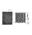
図6は、従来TFTの母材であるエキシマレーザーアニールにより形成した多結晶Si薄膜の表面SEM(走査電子顕微鏡)像である。
なお、この多結晶Si薄膜は、ガラス基板上に周知のプラズマCVD法によって膜厚50nmに成膜し、それをエキシマレーザーにより、エネルギー密度340mJ/cm2の条件でアニールしたものである。
【0031】
この低温poly-Siの平均粒径は50〜100nmと比較的小さめの例を挙げたが、現在到達できる最大粒径は200〜300nm程度である。しかし、粒径が大きくなるにしたがい粒径ばらつきも増大し、その結果TFT移動度に大きなばらつきが生じることが問題となっている。
【0032】
このため実用的な結晶粒径としては図に挙げた50〜100nmが典型例である。各結晶粒の粒界は暗いコントラストとなっているが、それに隣接した部分においてところどころ明るいコントラストの領域が見られる。このようなコントラストの違いは表面凹凸に相当する。
【0033】
エキシマレーザーアニールなどの熱処理法では溶融から固化する過程でSi結晶の体積膨張を伴う。このため各結晶粒がぶつかり合う粒界付近では膨張した体積分を逃がすために基板に垂直な上方向へ膜を持ち上げる力が働く。結晶粒界の3重点付近ではこの力がさらに大きくなり表面凹凸の原因となっている。膜厚50nmのSi多結晶に対し平均的表面凹凸は50nmにも達する。
【0034】
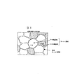
図7は、本発明の低温多結晶Si1-xGex薄膜の表面SEM像(左図)および平面TEM(透過電子顕微鏡)像である。Ge組成比はx=0.3、KrFエキシマレーザーエネルギー密度240mJ/cm2、30回照射により形成したものである。
【0035】
なお、この場合も多結晶Si薄膜は、ガラス基板上に周知のプラズマCVD法によって膜厚50nmに成膜したが、その際にCVDガス中にソースとしてGeをSiに対して30mol%導入し、Si0.7Ge0.3薄膜(以下、単にSiGe薄膜と略記)とした。それをエキシマレーザーにより、エネルギー密度240mJ/cm2の条件でアニールしたものである。
【0036】
図7の左図を見ると、結晶粒径は図6の多結晶Si薄膜のそれとほとんど同じであるが、粒内と粒界のコントラスト関係が反転していることがわかる。これは図6の場合とは逆に、粒界の方が粒内より上に凸となっていることが原因である。元素分析の結果、この粒界には粒内よりはるかに高濃度のGeが検出され、その高濃度領域と本図における明るいコントラスト領域とはほぼ一致した。
【0037】
この多結晶Si0.7Ge0.3薄膜の平面TEMの暗視野像(図7の右図)を見ると結晶構造の詳細を知ることができる。本図(図7の右図)では基板面に平行な{110}面が明るく表示されるような条件で測定されている。図を見るとほとんどの結晶粒は同じ明るさに揃っており、若干数の黒い粒が間に存在することがわかる。結晶粒内にはスタッキングフォールトか双晶と思われる直線上の模様がところどころ見えるがそれ意外はほぼきれいな単結晶となっていることがわかる。
【0038】
図8は、図7に示した本発明の低温多結晶SiGe薄膜の結晶構造模式図である。大部分の結晶粒が基板に平行な{110}面を持って揃っており、若干数の面方位の異なる粒が間に存在している。これら面方位の異なる粒は条件を変えたTEM観察によって、{110}面が基板平行面から1〜10度傾いたものであることがわかっている。このため本発明の多結晶SiGe薄膜は基本的に{110}面方位を持った多結晶であることがわかる。各粒内はアニール前に導入していたGe組成比よりSi-richであり、粒界ではそれに対しGe組成比の大きな結晶となっている。
【0039】
このような相分離(Ge組成比が結晶粒内と粒界とで異なる)が起こる原因は、Si中におけるGeの拡散係数とSi対Geの結合エネルギーに起因している。非晶質Si中のGe拡散係数は比較的大きく600℃でもD=8.0×10⁻²⁰[m2/s]である(文献S. M. Prokes and F. Spaepen, Appl. Phys. Lett., vol 47, p234 (1985)参照)。
【0040】
このような移動条件のもと結晶が安定な格子を組むためには、各原子間の結合エネルギーを最小化した方がよい。Si-Si、Si-Ge、Ge-Ge間の結合エネルギーはそれぞれ3.73eV、3.65eV、3.56eVである(文献K. Nakagawa, N. Sugii, S. Yamaguchi, and M. Miyao, J. Cryst. Growth, vol 210, p560, (1999)参照)。
【0041】
このためGeはSiと結合するよりGe同士で結合する方がエネルギー的に安定となる。アニール前にSiの方がGeより多い条件に設定しておくと、結晶化の初期段階である任意の場所にSi結晶核ができ、それが成長する過程においてGeを周辺に追い出しながらSiを多く内包した結晶粒が成長する。このような結晶粒がいたるところ成長することにより、上述のような結晶構造を持つ多結晶SiGeが形成されると思われる。
【0042】
このような複数種からなる元素間の相分離自体は従来から知られている。相分離した元素それぞれをp型/n型に切り分けることで多結晶薄膜を熱電変換材料に利用した例もある(例えば特開平2000-261043号公報)。しかし、本発明の多結晶SiGe薄膜のように粒界構造のいたるところできれいにGe-richとなり、以下で述べるように粒界における表面凹凸を抑制できTFTに応用できる多結晶SiGe薄膜はこれまで知られていない。
【0043】
また、このようにGe-richな相ができると特に正孔移動度にとって有利な構造となる。材料自体の性質として単結晶Ge(電子移動度〜3000cm2/Vs、正孔移動度〜1500cm2/Vs)は、単結晶Si(電子移動度〜1500cm2/Vs、正孔移動度〜500cm2/Vs)より大きな移動度を持っている(文献M. V. Fischetti and S. E. Laux, J. Appl. Phys. Vol 80, p2234, (1996)参照)。
【0044】
従来問題視されてきたGe/酸化膜界面安定性の問題も熱酸化膜ではなく堆積酸化膜であればそれほど問題ではないこともわかっている。このような潜在能力の高いGeがTFTで用いられていない理由は形成できる多結晶Geの粒径が極めて小さく粒界散乱が大きくて実用にならないからである。しかし本発明のような多結晶SiGe薄膜構造であれば粒径は多結晶Si薄膜のそれに匹敵し、散乱の大きい粒界付近に高移動度のGe-rich相が存在することにより全体として高移動度を実現できるという利点がある。
【0045】
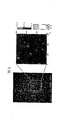
図9は、従来の多結晶Si薄膜のSEM像(左図)の四角領域におけるAFM(原子間力顕微鏡)像(右図)である。このAFM像は表面凹凸をそのまま直接コントラスト比で表示している。多結晶Si薄膜における結晶粒の3重点付近でいたるところ明るい凸部が見られる。これら凸部の頂点と凹部の底との高低差は上述したように約50nmと非常に大きい。これは体積膨張によって働く上向きの力が3重点で極めて大きいためである。
【0046】
一方、図10は、本発明の多結晶SiGe薄膜のSEM像(左図)、およびその四角領域におけるAFM像(右図)である。AFM像を見れば明らかなように粒界に相当する部分でまんべんなく明るく、凸部が形成されていることがわかる。
【0047】
図11の左図は、上記図10の右図と同様のAFM像であるが、右図はその直線部分における高低差分布を示す図である。この図から明るい部分が凸部、暗い部分が凹部に相当することがはっきりわかる。この凸部の頂点と凹部の底との高低差は最大で20nm程度と上述の図7に示した多結晶Si薄膜の50nmと比較して大幅に抑制されていることがわかる。
【0048】
これは主としてSi、Ge間で体積膨張係数や弾性係数が異なることが原因と考えられる。つまり、アニール前には非晶質SiGe混晶としての格子定数(>非晶質Si)で薄膜が形成されていたが、固化する際の相分離によって比較的硬いSi結晶の周りに柔らかいGe-rich相が形成されることで体積膨張分を粒界で緩和でき、その結果表面凹凸を抑制できていると考えられる。いずれにしても本発明の多結晶SiGe薄膜は、従来の多結晶Si薄膜より非常に小さな表面凹凸しか持たないことがわかる。
【0049】
図12は、本発明の多結晶SiGe薄膜を形成するために必要なレーザーアニール条件を、Ge組成比x=0.3の場合を例に示したものである。横軸は、エキシマ(KrF)レーザーのエネルギー密度[mJ/cm2]、縦軸は多結晶SiGe薄膜の膜厚(nm)であり、照射回数はすべて30回である。エネルギー密度を最低の140[mJ/cm2]から徐々に増大させていくと、表面凸部を示す明るいコントラスト領域がしだいに増していく。
【0050】
このうち膜厚50nmおよび30nmの場合だけ、それぞれ240[mJ/cm2]、220[mJ/cm2]で特異的に凸部が結晶粒界構造に一致することがわかる。このような構造は他のGe組成比(たとえばx=0.1など)でも見ることができるが、いずれの場合も極めて狭いアニール条件においてしか実現できないことがわかっている。この原因は、アニール前に導入したGe濃度が固化過程でちょうど偏析できる条件がそれほど広くないことによるためと思われるが、本発明ではこれら特異的なアニール処理条件で実現する多結晶SiGe薄膜を有効利用する。
以上で本発明の特徴である多結晶SiGe薄膜の結晶成長特性についての説明を終わる。以下では本発明の実施例に関する説明を行。
【0051】
【実施例】
以下、図1〜図5を用いて本発明の実施例を具体的に説明する。
(実施例1)
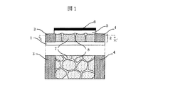
図1は、本発明の第1の実施例に係わる薄膜tランジスタ装置の展開図である。上段が縦断面図、その下段はチャネル部分を横(X−X‘方向)に切断した平面図である。ガラス板からなる絶縁体基板1上に、下記のプラズマCVDによる成膜条件、及びレーザーアニール条件で多結晶Si1-xGex薄膜2を形成した。
【0052】
すなわち、原料ガスとして、シラン及びゲルマンを用い、Si対Geの流量比が0.7対0.3になるようにガス量を調整しながら、合計膜厚が50nmとなるようプラズマCVDにより非晶質Si1-xGex薄膜を形成した。
【0053】
次に、成膜した表面に対し、レーザーアニール条件としてエネルギー密度240[mJ/cm2]、パルス数30回、パルス周波数100Hzでエキシマレーザーを照射し、多結晶Si1-xGex薄膜2を形成した。
【0054】
この多結晶Si1-xGex薄膜には、ソース3、ドレイン4、およびチャネル上にゲート絶縁膜5、ゲート6が形成されている。チャネルのうち、特にゲート絶縁膜5直下の領域は電界効果トランジスタの活性領域であり電流密度が最も大きい。その部分の平面図が図1の下段の図に描かれているが、本実施例ではこの平面上における多結晶Si1-xGex薄膜の結晶粒7内部のGe組成比xを0<x≦0.1、結晶粒界8におけるGe組成比xを0.3≦x<1とした。
【0055】
このような格子構造をとると、上述したように結晶粒界8の表面(凸部)と結晶粒7の表面(凹部)との高低差が20nm程度と大幅に抑制されて、ゲート絶縁膜5を比較的薄く(〜50nm)することができる。このため比較的小さなゲート電圧で多くのキャリアをチャネルに誘起することができ高移動度を実現できる。
【0056】
また、結晶粒7の大半が基板1に平行な{110}面に揃っていることで結晶粒界8の格子整合が比較的整いキャリアの粒界散乱を抑制できる効果も持つ。さらに、粒界8に高移動度のGe-rich相が形成されていることで膜全体の移動度が向上されるという利点も持つことが本実施例の特徴である。
【0057】
なお、多結晶Si1-xGex薄膜中のSiに対するGe組成比xの測定は、以下の方法で行った。
透過型電子顕微鏡(TEM)内に備えたX線微量分析計のプローブ用の電子ビームを小さく(約100nm)絞って試料表面に照射し、照射された領域から放出される特性X線の波長と強度を測定することにより、SiとGeとの濃度を測定する。
次に、このSiとGeとの濃度の測定結果から計算により、Siに対するGe組成比xを求める。
【0058】
また、結晶粒の組成比の測定は、ビーム照射領域が結晶粒内部に納まるように行う。粒界の組成比の測定は、ビーム照射領域が粒界を含むように行う。ここで、ビーム照射領域が粒界からはみ出して結晶粒にまたがっても良い。
(実施例2)
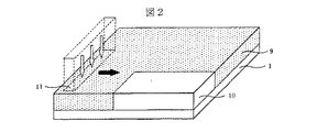
図2〜図4は、本発明の第2の実施例に係わる薄膜半導体装置とその製造過程を模式的に示したものである。本実施例では多結晶Si1-xGex薄膜を部分的に導入してトランジスタをCMOS(相補型MOS)化するものである。
【0059】
まず、図2に示したように、絶縁体基板(ガラス板)1上に非晶質Si薄膜9を形成する。その一部を通常のフォトプロセスでエッチング除去し、埋め込み型のGe組成比増加領域10を設ける。このようにして得た薄膜表面をKrFエキシマレーザーで照射しつつ、基板1を保持したステージを順次移動させることでレーザービーム照射領域11を走査させる。このとき予めステージ移動領域をプログラム制御することで、後にトランジスタ領域となる部分だけを選択的に結晶化する。
【0060】
このようにして、図3に示したように非晶質Si薄膜9の必要領域にのみ、純粋Si多結晶12および多結晶Si1-xGex薄膜2領域が形成される。
【0061】
次に、図4に示したように、結晶化した薄膜にAsイオンを注入することでn型領域14を、また、Bイオンを注入することでp型領域13を、それぞれ注入用マスクを使用して順序よくかつ領域選択的に形成する。この後窒素雰囲気中で600℃1時間程度の炉アニールを行いn型領域14およびp型領域13のキャリア活性化を行い、その上にゲート絶縁膜5、ゲート6を設けてトランジスタを形成する。
【0062】
こうすることでp型領域13には、多結晶Si薄膜12からなるnタイプトランジスタが、また、n型領域14には、多結晶Si1-xGex薄膜2からなるpタイプトランジスタがそれぞれでき、低消費電力と高移動度を両立させたCMOS型トランジスタが形成されるという利点がある。
(実施例3)
図5は、本発明の薄膜半導体装置を利用した画像表示装置の分解組み立て図の例を示す。絶縁体基板(ガラス板)1上に多結晶Si薄膜と多結晶Si1-xGex薄膜を選択的に形成し、その上に画素ドライバ領域17、バッファアンプ領域18、ゲートドライバ領域19、シフトレジスタ領域20、データドライバ領域21などからなる回路が集積されており、それらが一体となって、画素16を持つ画像表示パネル15に接続されて機能する。
【0063】
これらの回路を構成するトランジスタには要求される性能がそれぞれ異なるため、本発明の実施例1〜3のトランジスタが選択的かつ複合的に組み合わされて利用されている。このような構成では、大面積のガラス基板上に主要な回路を集積することができ、従来の周辺回路のほとんどを集積した画像表示装置を形成することができる。さらに低コストのガラス基板を用いて数少ない工程により製造できるという利点がある。
【0064】
【発明の効果】
本発明によれば、Si中にGeを導入し結晶化に伴う相分離で結晶粒内と結晶粒界との間にGe組成比を異ならせることで、結晶粒界におけるキャリア散乱要因を抑制し、かつ結晶の体積差を利用して表面凹凸を抑制することにより高移動度TFTを実現する。これにより、同一ガラス基板上に、画素部、周辺回路を集約的に形成することが可能となるため、大面積(例えば15インチ以上)画像表示装置を高集積化することができる。
【図面の簡単な説明】
【図1】本発明の第1の実施例に係わる薄膜トランジスタ装置の展開図である。上段が縦断面図、その下段はチャネル部分を横に切断した平面図である。
【図2】本発明の第2の実施例に係わる薄膜トランジスタ装置とその製造過程を模式的に示したものである。
【図3】同じく本発明の第2の実施例に係わる薄膜トランジスタ装置とその製造過程を模式的に示したものである。
【図4】同じく本発明の第2の実施例に係わる薄膜トランジスタ装置とその製造過程を模式的に示したものである。
【図5】本発明の薄膜トランジスタ装置を利用した画像表示装置の例を示したものである。
【図6】従来TFTの母材であるエキシマレーザーアニールにより形成した多結晶Si薄膜の表面SEM(走査電子顕微鏡)像である。
【図7】本発明の多結晶SiGe薄膜の表面SEM像(左図)および平面TEM(透過電子顕微鏡)像である。
【図8】本発明の多結晶SiGe薄膜の結晶構造模式図である。
【図9】従来多結晶Si薄膜のSEM像(左図)とその四角領域におけるAFM(原子間力顕微鏡)像(右図)である。
【図10】本発明の多結晶SiGe薄膜のSEM像(左図)とその四角領域におけるAFM像(右図)である。
【図11】上記図10のAFM像(左図)と、その直線部分における高低差分布を示す図(右図)である。
【図12】本発明の多結晶Si1-xGex薄膜を形成するために必要なレーザーアニール条件を、Ge組成比x=0.3の場合で示したものである。
【符号の説明】
1…絶縁体基板、
2…多結晶Si1-xGex薄膜、
3…ソース、
4…ドレイン、
5…ゲート絶縁膜、
6…ゲート、
7…結晶粒、
8…結晶粒界、
9…非晶質Si薄膜、
10…Ge組成比増加領域、
11…レーザービーム照射領域、
12…純粋Si多結晶、
13…p型領域、
14…n型領域、
15…画像表示パネル、
16…画素、
17…画素ドライバ領域、
18…バッファアンプ領域、
19…ゲートドライバ領域、
20…シフトレジスタ領域、
21…データドライバ領域。[0001]
BACKGROUND OF THE INVENTION
The present invention relates to a thin film transistor device and a manufacturing method thereof, and more particularly to a thin film transistor device suitable for a transistor using a polycrystalline silicon (poly-Si) thin film and a manufacturing method thereof.
[0002]
[Prior art]
The thin film transistor device is used as a pixel or a peripheral circuit driving thin film transistor (TFT) mainly in an image display device such as a liquid crystal display device (LCD) or a plasma display device (PDP).
[0003]
High-temperature polycrystalline Si has been mainly used for a base thin film on which a conventional thin film transistor is formed. This is a polycrystalline Si (poly-Si) thin film formed on a quartz substrate, which is an insulator substrate, by high-temperature heat treatment at around 900 ° C. Polycrystalline Si with a relatively large grain size (eg 500-600 nm) It is formed.
[0004]
A TFT formed on this high-temperature polycrystalline Si (hereinafter referred to as high-temperature poly-Si) thin film has a field effect mobility of 100 to 100 in order to use a Si thin film with low grain boundary density and good crystallinity as a channel. 150 [cm 2 / Vs] and that of conventional Si-LSi on Si substrate (~ 500 [cm 2 / Vs], literature SM Sze, Physics of Semiconductor Devices, p. 29, Second Edition, Wiley).
[0005]
However, this high-temperature poly-Si requires the use of an expensive quartz substrate as an insulating substrate so that it can withstand high-temperature processes. Therefore, it is difficult to reduce the cost of the entire semiconductor device due to the substrate cost. Was restricted.
[0006]
In recent years, low temperature polycrystalline Si (hereinafter referred to as low temperature poly-Si) has been actively studied as an alternative. This is polycrystalline Si obtained by crystallizing amorphous Si formed on a low-cost glass substrate or plastic substrate by a process such as plasma CVD using a melt recrystallization method such as excimer laser annealing. When this method is used, a polycrystalline Si thin film can be formed at a low temperature (up to 150 ° C.), so that there is an advantage that a very inexpensive TFT can be formed.
[0007]
However, conventional low-temperature poly-Si can only form polycrystalline Si having a smaller crystal grain size (˜100 nm) and larger surface roughness (˜50 nm) than high-temperature poly-Si.
[0008]
When the crystal grain size is small, the grain boundary density existing in the carrier path increases, and there is a disadvantage that the carrier mobility is lowered through grain boundary scattering.
In addition, if the surface irregularities are large, it is necessary to increase the thickness of the gate insulating film (˜100 nm) in order to suppress the gate leakage current. Carrier mobility is reduced.
[0009]
For this reason, in the conventional product-based TFT using low-temperature poly-Si as the element material, the field-effect mobility is ~ 150 [cm when the electron carrier is used. 2 / Vs], ~ 50 [cm for hole carriers 2 / Vs]. Since such a low mobility cannot reach the required element speed, there arises a problem that the types of elements that can be formed on the same glass (or plastic) substrate are limited.
[0010]
For example, in the case of an image display device, a pixel circuit unit having relatively low required performance can be formed on glass (or plastic), but other high-required performance circuit such as a source driver, gate driver, shift register, peripheral controller, Since it cannot be formed on the same substrate, it must be integrated on a printed circuit board as a semiconductor chip using conventional Si-LSI technology and used by connecting it to a glass substrate.
[0011]
In such a method, there is a problem that the screen size is reduced (4 inches to 10 inches) depending on the area where the peripheral circuit portion is mounted, and the cost of the entire image display apparatus becomes very high. Furthermore, in power-saving image display devices with promising future markets, it is essential to use CMOS (complementary MOS) TFTs. To that end, it is expected that the required performance for the field-effect mobility of hole carriers will increase further. Is done.
[0012]
In order to improve such problems, technology is required to improve the performance of TFTs by realizing a polycrystalline thin film that can suppress the grain boundary scattering of low-temperature poly-Si and reduce the surface roughness. . Various techniques have been proposed so far to improve the functionality of low-temperature poly-Si as described below.
[0013]
For example, a metal element that selectively promotes crystallization is introduced into an amorphous Si film formed on an insulator substrate, and crystal growth is performed in a direction parallel to the substrate. 111] Technology for forming polycrystalline Si with an axis (for example, Japanese Patent Laid-Open No. 7-321339); the shape of the beam for heat treatment and the amount of irradiation position movement are precisely controlled, and the <100> axis Technology for forming a rectangular polycrystalline Si having {220} plane parallel to the scanning direction (or 45 ° angle) (for example, Japanese Patent Laid-Open No. 10-41234); a first polycrystalline Si layer on a substrate Forming a seed crystal having one of specific surfaces ({100}, {110}, {111}) by anisotropic etching, and forming a second polycrystalline Si layer thereon, A technique for forming a columnar polycrystalline Si layer having a uniform plane orientation (for example, JP-A-8-55808).
However, despite these many attempts, it has not been possible to obtain a sufficiently high mobility TFT.
[0014]
[Problems to be solved by the invention]
None of the above conventional crystallization methods of low-temperature poly-Si thin films are sufficiently completed, and any of the maximum grain size and surface irregularities that can be reached is required for peripheral circuit integrated liquid crystal display panels, for example. It does not reach the required performance of TFT. For this reason, these technologies do not sufficiently replace existing low-function thin film transistor devices. Therefore, the technical problem of realizing a high-performance and large-area image display device at a low cost is extremely important.
[0015]
Therefore, the first object of the present invention is to achieve high mobility for hole carriers by suppressing carrier scattering at crystal grain boundaries and reducing surface irregularities in low-temperature poly-Si, which is a TFT element material. It is to provide a thin film transistor device having excellent characteristics that cannot be obtained by the prior art by realizing a polycrystalline thin film having such a crystal structure, and a second purpose is to easily obtain this thin film transistor device. A third object is to provide an image display device using the thin film transistor device.
[0016]
[Means for Solving the Problems]
In order to achieve the above object, the present inventors conducted various experimental studies on low-temperature poly-Si for forming TFTs. As a result, Ge was introduced into the poly-Si thin film and crystal grains were separated by phase separation accompanying crystallization. By making the Ge composition ratio different between the inside and the grain boundary (specifically, making the Ge composition ratio of the grain boundary larger than the portion where the Ge composition is smallest in the grain), the carriers at the grain boundary An important finding has been obtained that a high mobility TFT can be realized by suppressing scattering factors and suppressing surface irregularities by utilizing the volume difference of crystals.
[0017]
The present invention has been made based on such knowledge, and the first object is to form an insulator substrate, a polycrystalline thin film formed on the insulator substrate, and the polycrystalline thin film. A transistor composed of a source, a drain, a channel, and a gate, and the polycrystalline thin film in the channel portion of the transistor is made of silicon germanium polycrystalline Si 1-x Ge x Provided that the composition ratio x of Ge to Si is 0 <x <1, and the composition ratio x of Ge in the polycrystalline thin film is a grain boundary more than the portion where the Ge composition is minimum in the crystal grain. Achieved by a thin film transistor device characterized in that
[0018]
Preferably, the thickness of the polycrystalline thin film is 10 to 100 nm, the composition ratio x of Ge in the central part of the crystal grains constituting the polycrystalline thin film is 0 <x ≦ 0.3, and Ge The composition ratio x is 0.1 ≦ x <1.0, and the Ge composition ratio x is always larger at the grain boundary than the portion where the Ge composition is minimum in the crystal grain.
[0019]
Further features of the thin film transistor device of the present invention are listed below.
In the above thin film transistor device, polycrystalline Si 1-x Ge x The thin film is characterized in that the surface unevenness at the grain boundary is 30 nm or less.
[0020]
In the thin film transistor device, the main carrier flowing in the channel portion of the transistor is a hole.
[0021]
The thin film transistor device includes an insulator substrate, a polycrystalline thin film formed on the insulator substrate, and a transistor including a source, a drain, a channel, and a gate formed on the polycrystalline thin film. The crystal thin film in the channel portion has a {110} crystal plane parallel to the substrate, and the average lattice constant at the grain boundary is larger than the average lattice constant inside the crystal grain.
[0022]
The thin film transistor device includes an insulator substrate and polycrystalline Si formed on the insulator substrate. 1-x Ge x Thin film, where the composition ratio x of Ge to Si is 0 <x <1, and the polycrystalline Si 1-x Ge x And a circuit portion formed by integrating a plurality of transistors each having a source, drain, channel, and gate formed on a thin film, and the circuit portion includes both a p-type transistor and an n-type transistor. A CMOS transistor is included.
[0023]
The thin film transistor device is characterized in that the Ge composition ratio x of the p-type transistor constituting the circuit portion is larger than the Ge composition ratio of the n-type transistor.
[0024]
The second purpose is to form an amorphous Si1-xGe film with a thickness of 10 to 100 nm on an insulator substrate. x Forming a layer, wherein the composition ratio x of Ge to Si is 0 <x <1, and the amorphous Si1-xGe x The layer has an energy density of 200-300mJ / cm 2 And a heat treatment step of crystallizing with an excimer laser having 1 to 50 pulses. This is achieved by a method of manufacturing a thin film transistor device.
[0025]
Preferably, in the method of manufacturing the thin film transistor device, the heat treatment step includes the amorphous Si1-xGe. x When the layer thickness is Tnm, the energy density is (180 + T) to (200 + T) mJ / cm 2 As described above, it is characterized by being changed in accordance with the film thickness.
[0026]
The third object is to control an image display unit, display of the image display unit, an image display circuit including at least a data driver, a gate driver, and a buffer amplifier, and the image located at the periphery of the image display circuit. An image display device having a peripheral circuit unit for controlling a display circuit, wherein the image display circuit and the peripheral circuit unit are integrated on the same substrate as the substrate constituting the image display unit, and the image The display circuit and the peripheral circuit unit are formed of an insulator substrate and polycrystalline Si formed on the insulator substrate. 1-x Ge x Thin film, where the composition ratio x of Ge to Si is 0 <x <1, and the polycrystalline Si 1-x Ge x A circuit portion formed by integrating a plurality of transistors each having a source, drain, channel, and gate formed on a thin film, and the circuit portion is either a p-type transistor or an n-type transistor, or This is achieved by an image display device including a CMOS transistor in which both are mixed.
[0027]
Preferably, in the image display device, a Ge composition ratio x of a p-type transistor constituting the circuit unit is larger than a Ge composition ratio of an n-type transistor.
[0028]
More preferably, the circuit portion holds an alignment mark provided in the vicinity of the circuit in order to distinguish one of the p-type transistor, the n-type transistor, and the CMOS-type transistor. To do.
[0029]
DETAILED DESCRIPTION OF THE INVENTION
Hereinafter, SiGe crystal growth characteristics, which are the characteristics of the present invention, will be described in detail in comparison with the prior art using FIGS. In the present specification, crystallographically equivalent plane orientation groups such as crystal plane orientations (110), (101), (011) are collectively expressed as {110}.
[0030]
FIG. 6 is a surface SEM (scanning electron microscope) image of a polycrystalline Si thin film formed by excimer laser annealing, which is a base material of a conventional TFT.
This polycrystalline Si thin film is formed on a glass substrate to a film thickness of 50 nm by a well-known plasma CVD method, and the energy density is 340 mJ / cm by an excimer laser. 2 Annealed under the following conditions.
[0031]
Although the average particle size of this low-temperature poly-Si is relatively small, 50 to 100 nm, the maximum particle size that can be reached at present is about 200 to 300 nm. However, as the particle size increases, the particle size variation also increases, and as a result, a large variation in TFT mobility occurs.
[0032]
For this reason, 50-100 nm shown in the figure is a typical example of a practical crystal grain size. Although the grain boundary of each crystal grain has a dark contrast, a bright contrast region is sometimes seen in a portion adjacent to the grain boundary. Such a difference in contrast corresponds to surface irregularities.
[0033]
Heat treatment methods such as excimer laser annealing involve volume expansion of Si crystals during the process of melting from solidification. For this reason, in the vicinity of the grain boundary where the crystal grains collide, a force for lifting the film upward works perpendicular to the substrate in order to escape the expanded volume. In the vicinity of the triple point of the grain boundary, this force is further increased, causing surface irregularities. The average surface roughness of the Si polycrystal with a thickness of 50 nm reaches 50 nm.
[0034]
FIG. 7 shows the low temperature polycrystalline Si of the present invention. 1-x Ge x It is the surface SEM image (left figure) and planar TEM (transmission electron microscope) image of a thin film. Ge composition ratio is x = 0.3, KrF excimer laser energy density is 240mJ / cm 2 , Formed by 30 irradiations.
[0035]
In this case as well, the polycrystalline Si thin film was formed on the glass substrate to a film thickness of 50 nm by a known plasma CVD method. At that time, 30 mol% of Ge as a source was introduced into the CVD gas as a source, Si 0.7 Ge 0.3 A thin film (hereinafter simply abbreviated as SiGe thin film) was used. With an excimer laser, the energy density is 240mJ / cm 2 Annealed under the following conditions.
[0036]
As can be seen from the left diagram of FIG. 7, the crystal grain size is almost the same as that of the polycrystalline Si thin film of FIG. 6, but the contrast relationship between the grain interior and the grain boundary is reversed. Contrary to the case of FIG. 6, this is because the grain boundary is convex upward from the inside of the grain. As a result of elemental analysis, a much higher concentration of Ge was detected in the grain boundary than in the grain, and the high concentration region and the bright contrast region in this figure almost coincided.
[0037]
This polycrystalline Si 0.7 Ge 0.3 The details of the crystal structure can be known by looking at the dark field image (right figure in FIG. 7) of the thin-film planar TEM. In this figure (the right figure of FIG. 7), the measurement is performed under such a condition that the {110} plane parallel to the substrate surface is displayed brightly. As can be seen from the figure, most of the crystal grains are aligned with the same brightness, and a few black grains are present between them. In the crystal grains, there are some straight line patterns that seem to be stacking faults or twins.
[0038]
FIG. 8 is a schematic diagram of the crystal structure of the low-temperature polycrystalline SiGe thin film of the present invention shown in FIG. Most of the crystal grains are aligned with the {110} plane parallel to the substrate, and there are some grains with different plane orientations between them. These grains with different plane orientations are found by TEM observation under different conditions, with the {110} plane tilted 1 to 10 degrees from the substrate parallel plane. Therefore, it can be seen that the polycrystalline SiGe thin film of the present invention is basically a polycrystal having a {110} plane orientation. Each grain is Si-rich than the Ge composition ratio introduced before annealing, and the grain boundary is a crystal having a larger Ge composition ratio.
[0039]
The reason why such phase separation (Ge composition ratio is different between crystal grains and grain boundaries) is due to the diffusion coefficient of Ge in Si and the binding energy of Si to Ge. Ge diffusion coefficient in amorphous Si is relatively large, even at 600 ℃, D = 8.0 × 10 -20 [m 2 / s] (see SM Prokes and F. Spaepen, Appl. Phys. Lett., vol 47, p234 (1985)).
[0040]
In order for the crystal to form a stable lattice under such movement conditions, it is better to minimize the bond energy between the atoms. The bond energies between Si-Si, Si-Ge, and Ge-Ge are 3.73 eV, 3.65 eV, and 3.56 eV, respectively (references K. Nakagawa, N. Sugii, S. Yamaguchi, and M. Miyao, J. Cryst. Growth, vol 210, p560, (1999)).
[0041]
For this reason, Ge is more energetically stable when bonded to Ge rather than bonded to Si. If the condition of Si is larger than that of Ge before annealing, Si crystal nuclei are formed at an arbitrary position in the initial stage of crystallization, and while Si grows, Ge is expelled to the periphery and much Si is added. The included crystal grains grow. By growing such crystal grains everywhere, it is considered that polycrystalline SiGe having the crystal structure as described above is formed.
[0042]
Such phase separation itself between a plurality of elements has been conventionally known. There is also an example in which a polycrystalline thin film is used as a thermoelectric conversion material by cutting each phase-separated element into p-type / n-type (for example, JP-A-2000-261043). However, a polycrystalline SiGe thin film that can be applied to a TFT that can suppress surface irregularities at the grain boundary and can be applied to a TFT as described below, as shown in the following. Not.
[0043]
In addition, when such a Ge-rich phase is formed, a structure that is particularly advantageous for hole mobility is obtained. As a property of the material itself, single crystal Ge (electron mobility ~ 3000cm 2 / Vs, hole mobility ~ 1500cm 2 / Vs) is single crystal Si (electron mobility ~ 1500cm) 2 / Vs, hole mobility ~ 500cm 2 / Vs) (see literature MV Fischetti and SE Laux, J. Appl. Phys. Vol 80, p2234, (1996)).
[0044]
It has also been found that the Ge / oxide interface stability problem, which has been regarded as a problem in the past, is not so much a problem if it is a deposited oxide film rather than a thermal oxide film. The reason why such high potential Ge is not used in the TFT is that the polycrystalline Ge that can be formed has a very small grain size and large grain boundary scattering, which is not practical. However, the polycrystalline SiGe thin film structure as in the present invention has a grain size comparable to that of the polycrystalline Si thin film, and the high mobility as a whole is due to the presence of the Ge-rich phase with high mobility near the highly scattering grain boundary. The advantage is that the degree can be realized.
[0045]
FIG. 9 is an AFM (atomic force microscope) image (right diagram) in a square region of an SEM image (left diagram) of a conventional polycrystalline Si thin film. In this AFM image, surface irregularities are directly displayed as a contrast ratio. Bright convex portions are seen everywhere near the triple point of the crystal grains in the polycrystalline Si thin film. As described above, the difference in height between the apex of the convex portion and the bottom of the concave portion is as large as about 50 nm. This is because the upward force working by volume expansion is extremely large at the triple point.
[0046]
On the other hand, FIG. 10 shows an SEM image (left figure) of the polycrystalline SiGe thin film of the present invention and an AFM image (right figure) in the square region. As is clear from the AFM image, it can be seen that the portions corresponding to the grain boundaries are evenly bright and have convex portions.
[0047]
The left diagram of FIG. 11 is an AFM image similar to the right diagram of FIG. 10 above, but the right diagram is a diagram showing the height difference distribution in the straight line portion. From this figure, it can be clearly seen that the bright part corresponds to the convex part and the dark part corresponds to the concave part. It can be seen that the difference in height between the top of the convex portion and the bottom of the concave portion is about 20 nm at the maximum, which is greatly suppressed as compared with 50 nm of the polycrystalline Si thin film shown in FIG.
[0048]
This is presumably due to the difference in volume expansion coefficient and elastic coefficient between Si and Ge. In other words, before annealing, a thin film was formed with a lattice constant (> amorphous Si) as an amorphous SiGe mixed crystal, but soft Ge- around the relatively hard Si crystal due to phase separation during solidification. It is thought that the volume expansion can be relaxed at the grain boundary by forming a rich phase, and as a result, surface irregularities can be suppressed. In any case, it can be seen that the polycrystalline SiGe thin film of the present invention has much smaller surface irregularities than the conventional polycrystalline Si thin film.
[0049]
FIG. 12 shows an example of the laser annealing conditions necessary for forming the polycrystalline SiGe thin film of the present invention when the Ge composition ratio x = 0.3. The horizontal axis is the energy density of excimer (KrF) laser [mJ / cm 2 The vertical axis represents the film thickness (nm) of the polycrystalline SiGe thin film, and the number of times of irradiation is 30 times. Minimum energy density of 140 [mJ / cm 2 From the point of view, the bright contrast region showing the surface convexity gradually increases.
[0050]
Of these, 240 [mJ / cm each for film thickness 50nm and 30nm only 2 ], 220 [mJ / cm 2 ], It can be seen that the protrusions specifically match the grain boundary structure. Such a structure can be seen at other Ge composition ratios (for example, x = 0.1), but it has been found that in any case, it can be realized only under extremely narrow annealing conditions. This is probably because the Ge concentration introduced before annealing is not so wide as the conditions for segregation during the solidification process. In the present invention, the polycrystalline SiGe thin film realized under these specific annealing conditions is effective. Use.
This is the end of the description of the crystal growth characteristics of the polycrystalline SiGe thin film, which is a feature of the present invention. In the following description, examples of the present invention will be described.
[0051]
【Example】
Examples of the present invention will be specifically described below with reference to FIGS.
(Example 1)
FIG. 1 is a developed view of a thin film t transistor device according to a first embodiment of the present invention. The upper part is a longitudinal sectional view, and the lower part is a plan view in which the channel portion is cut horizontally (XX ′ direction). Polycrystalline Si is formed on an insulating
[0052]
That is, using silane and germane as source gases, adjusting the gas amount so that the flow rate ratio of Si to Ge is 0.7 to 0.3, and amorphous Si by plasma CVD so that the total film thickness becomes 50 nm. 1-x Ge x A thin film was formed.
[0053]
Next, energy density of 240 [mJ / cm as laser annealing conditions for the deposited surface 2 ], Irradiated with excimer laser with 30 pulses and 100Hz pulse frequency, 1-x Ge x A
[0054]
This polycrystalline Si 1-x Ge x In the thin film, a
[0055]
With such a lattice structure, as described above, the height difference between the surface (convex portion) of the crystal grain boundary 8 and the surface (concave portion) of the crystal grain 7 is greatly suppressed to about 20 nm, and the
[0056]
Further, since most of the crystal grains 7 are aligned on the {110} plane parallel to the
[0057]
Polycrystalline Si 1-x Ge x The Ge composition ratio x with respect to Si in the thin film was measured by the following method.
The electron beam for the probe of the X-ray microanalyzer provided in the transmission electron microscope (TEM) is narrowed down (about 100 nm) to irradiate the sample surface, and the wavelength of characteristic X-rays emitted from the irradiated region By measuring the strength, the concentration of Si and Ge is measured.
Next, the Ge composition ratio x with respect to Si is obtained by calculation from the measurement result of the concentration of Si and Ge.
[0058]
Further, the measurement of the composition ratio of the crystal grains is performed so that the beam irradiation region is within the crystal grains. The measurement of the grain boundary composition ratio is performed so that the beam irradiation region includes the grain boundary. Here, the beam irradiation region may protrude from the grain boundary and straddle the crystal grain.
(Example 2)
2 to 4 schematically show a thin film semiconductor device and its manufacturing process according to the second embodiment of the present invention. In this example, polycrystalline Si 1-x Ge x A thin film is partially introduced to make a transistor a CMOS (complementary MOS).
[0059]
First, as shown in FIG. 2, an amorphous Si thin film 9 is formed on an insulator substrate (glass plate) 1. A part thereof is etched away by a normal photo process to provide a buried Ge composition
[0060]
In this way, pure Si polycrystalline 12 and polycrystalline Si are formed only in the necessary region of the amorphous Si thin film 9 as shown in FIG. 1-x Ge x A
[0061]
Next, as shown in FIG. 4, an n-
[0062]
By doing so, an n-type transistor made of the polycrystalline Si thin film 12 is formed in the p-
(Example 3)
FIG. 5 shows an example of an exploded view of an image display device using the thin film semiconductor device of the present invention. Polycrystalline Si thin film and polycrystalline Si on insulator substrate (glass plate) 1 1-x Ge x A thin film is selectively formed, and a circuit composed of a
[0063]
Since the required performance of the transistors constituting these circuits is different, the transistors according to the first to third embodiments of the present invention are selectively used in combination. In such a configuration, main circuits can be integrated on a large-area glass substrate, and an image display device in which most conventional peripheral circuits are integrated can be formed. Furthermore, there is an advantage that it can be manufactured by few processes using a low-cost glass substrate.
[0064]
【The invention's effect】
According to the present invention, Ge is introduced into Si and the Ge composition ratio is varied between the crystal grains and the crystal grain boundaries by phase separation accompanying crystallization, thereby suppressing the carrier scattering factor at the crystal grain boundaries. In addition, a high mobility TFT is realized by suppressing surface irregularities by utilizing the volume difference of crystals. Accordingly, the pixel portion and the peripheral circuit can be collectively formed on the same glass substrate, so that a large area (for example, 15 inches or more) image display device can be highly integrated.
[Brief description of the drawings]
FIG. 1 is a development view of a thin film transistor device according to a first embodiment of the present invention. The upper stage is a vertical cross-sectional view, and the lower stage is a plan view of a channel portion cut laterally.
FIG. 2 schematically illustrates a thin film transistor device according to a second embodiment of the present invention and a manufacturing process thereof.
FIG. 3 schematically shows a thin film transistor device according to a second embodiment of the present invention and its manufacturing process.
FIG. 4 schematically shows a thin film transistor device according to a second embodiment of the present invention and a manufacturing process thereof.
FIG. 5 shows an example of an image display device using the thin film transistor device of the present invention.
FIG. 6 is a surface SEM (scanning electron microscope) image of a polycrystalline Si thin film formed by excimer laser annealing, which is a base material of a conventional TFT.
FIG. 7 is a surface SEM image (left figure) and a planar TEM (transmission electron microscope) image of a polycrystalline SiGe thin film of the present invention.
FIG. 8 is a schematic diagram of a crystal structure of a polycrystalline SiGe thin film of the present invention.
FIG. 9 is an SEM image (left diagram) of a conventional polycrystalline Si thin film and an AFM (atomic force microscope) image (right diagram) in the square region.
FIG. 10 is an SEM image (left figure) of the polycrystalline SiGe thin film of the present invention and an AFM image (right figure) in the square region.
11 is a diagram (right diagram) showing the AFM image (left diagram) of FIG. 10 and the height difference distribution in the straight line portion thereof. FIG.
FIG. 12: Polycrystalline Si of the present invention 1-x Ge x Laser annealing conditions necessary for forming a thin film are shown in the case where the Ge composition ratio x = 0.3.
[Explanation of symbols]
1 ... Insulator substrate,
2 ... Polycrystalline Si 1-x Ge x Thin film,
3 ... Sauce,
4 ... drain,
5 ... Gate insulating film,
6 ... Gate,
7 ... crystal grains,
8 ... Grain boundary,
9: Amorphous Si thin film,
10: Ge composition ratio increasing region,
11 ... Laser beam irradiation area,
12 ... Pure Si polycrystal,
13 ... p-type region,
14 ... n-type region,
15 ... Image display panel,
16 ... Pixels,
17 ... pixel driver area,
18: Buffer amplifier area,
19: Gate driver area,
20: Shift register area,
21: Data driver area.
Claims (4)
Priority Applications (6)
| Application Number | Priority Date | Filing Date | Title |
|---|---|---|---|
| JP2001025531A JP4358998B2 (en) | 2001-02-01 | 2001-02-01 | Thin film transistor device and manufacturing method thereof |
| TW090103950A TW478171B (en) | 2001-02-01 | 2001-02-21 | Thin film semiconductor device and method for producing thereof |
| US09/790,545 US6521909B2 (en) | 2001-02-01 | 2001-02-23 | Thin film semiconductor device containing polycrystalline Si-Ge alloy and method for producing thereof |
| KR1020010009646A KR100761619B1 (en) | 2001-02-01 | 2001-02-26 | Thin film semiconductor device and method for producing thereof |
| US10/274,995 US6690064B2 (en) | 2001-02-01 | 2002-10-22 | Thin-film semiconductor device containing poly-crystalline Si-Ge alloy and method for producing thereof |
| US10/277,140 US6716726B2 (en) | 2001-02-01 | 2002-10-22 | Thin film semiconductor device containing polycrystalline Si—Ge alloy and method for producing thereof |
Applications Claiming Priority (1)
| Application Number | Priority Date | Filing Date | Title |
|---|---|---|---|
| JP2001025531A JP4358998B2 (en) | 2001-02-01 | 2001-02-01 | Thin film transistor device and manufacturing method thereof |
Publications (3)
| Publication Number | Publication Date |
|---|---|
| JP2002231958A JP2002231958A (en) | 2002-08-16 |
| JP2002231958A5 JP2002231958A5 (en) | 2006-03-30 |
| JP4358998B2 true JP4358998B2 (en) | 2009-11-04 |
Family
ID=18890502
Family Applications (1)
| Application Number | Title | Priority Date | Filing Date |
|---|---|---|---|
| JP2001025531A Expired - Fee Related JP4358998B2 (en) | 2001-02-01 | 2001-02-01 | Thin film transistor device and manufacturing method thereof |
Country Status (4)
| Country | Link |
|---|---|
| US (3) | US6521909B2 (en) |
| JP (1) | JP4358998B2 (en) |
| KR (1) | KR100761619B1 (en) |
| TW (1) | TW478171B (en) |
Families Citing this family (21)
| Publication number | Priority date | Publication date | Assignee | Title |
|---|---|---|---|---|
| JP3980159B2 (en) * | 1998-03-05 | 2007-09-26 | 株式会社半導体エネルギー研究所 | Method for manufacturing semiconductor device |
| JP3737914B2 (en) * | 1999-09-02 | 2006-01-25 | 松下電器産業株式会社 | Semiconductor device and manufacturing method thereof |
| US6882012B2 (en) * | 2000-02-28 | 2005-04-19 | Semiconductor Energy Laboratory Co., Ltd. | Semiconductor device and a method of manufacturing the same |
| JP3559962B2 (en) * | 2000-09-04 | 2004-09-02 | 日本航空電子工業株式会社 | Thermoelectric conversion material and method for producing the same |
| US6746942B2 (en) * | 2000-09-05 | 2004-06-08 | Sony Corporation | Semiconductor thin film and method of fabricating semiconductor thin film, apparatus for fabricating single crystal semiconductor thin film, and method of fabricating single crystal thin film, single crystal thin film substrate, and semiconductor device |
| JP2003332350A (en) | 2002-05-17 | 2003-11-21 | Hitachi Ltd | Thin film semiconductor device |
| JP3904512B2 (en) * | 2002-12-24 | 2007-04-11 | シャープ株式会社 | SEMICONDUCTOR DEVICE, ITS MANUFACTURING METHOD, AND ELECTRONIC DEVICE PROVIDED WITH SEMICONDUCTOR DEVICE |
| JP2004207616A (en) * | 2002-12-26 | 2004-07-22 | Hitachi Displays Ltd | Display |
| KR100975523B1 (en) * | 2003-12-30 | 2010-08-13 | 삼성전자주식회사 | Semiconductor device with modified mobility and thin film transistor having the same |
| JP4567984B2 (en) | 2004-01-30 | 2010-10-27 | 株式会社 日立ディスプレイズ | Flat panel display manufacturing equipment |
| KR100623689B1 (en) * | 2004-06-23 | 2006-09-19 | 삼성에스디아이 주식회사 | Thin Film Transitor and Method of fabricating thereof |
| JP5152827B2 (en) | 2007-03-22 | 2013-02-27 | 株式会社日立製作所 | THIN FILM TRANSISTOR AND ORGANIC EL DISPLAY DEVICE USING THE SAME |
| JP5648252B2 (en) * | 2010-08-27 | 2015-01-07 | 学校法人東北学院 | Semiconductor device |
| KR101983157B1 (en) * | 2013-11-19 | 2019-05-28 | 삼성전기주식회사 | Printed circuit board and method of manufacturing the same |
| NZ723384A (en) | 2014-03-12 | 2019-11-29 | Hexion Inc | Polymers, composites, and methods for making polymers and composites |
| CN108141215B9 (en) | 2015-07-29 | 2020-11-06 | 电路种子有限责任公司 | Complementary current field effect transistor device and amplifier |
| WO2017019978A1 (en) | 2015-07-30 | 2017-02-02 | Circuit Seed, Llc | Low noise trans-impedance amplifiers based on complementary current field-effect transistor devices |
| US10514716B2 (en) | 2015-07-30 | 2019-12-24 | Circuit Seed, Llc | Reference generator and current source transistor based on complementary current field-effect transistor devices |
| WO2017019973A1 (en) | 2015-07-30 | 2017-02-02 | Circuit Seed, Llc | Multi-stage and feed forward compensated complementary current field effect transistor amplifiers |
| CN111816610A (en) * | 2015-12-14 | 2020-10-23 | 电路种子有限责任公司 | Field effect transistor |
| CN107359203A (en) | 2017-05-12 | 2017-11-17 | 惠科股份有限公司 | Display panel and display device |
Family Cites Families (11)
| Publication number | Priority date | Publication date | Assignee | Title |
|---|---|---|---|---|
| KR940010378A (en) * | 1992-10-19 | 1994-05-26 | 김광호 | Method of manufacturing polycrystalline silicon thin film |
| JP2791858B2 (en) | 1993-06-25 | 1998-08-27 | 株式会社半導体エネルギー研究所 | Semiconductor device manufacturing method |
| JPH0823160A (en) * | 1994-05-06 | 1996-01-23 | Seiko Epson Corp | Method for bonding printed board with electronic component |
| JPH07321323A (en) * | 1994-05-24 | 1995-12-08 | Matsushita Electric Ind Co Ltd | Thin film transistor and its manufacturing method |
| JP3294439B2 (en) | 1994-08-17 | 2002-06-24 | 沖電気工業株式会社 | Method of forming polycrystalline silicon thin film |
| JP4026191B2 (en) | 1996-05-22 | 2007-12-26 | ソニー株式会社 | Method for forming silicon single crystal particles and method for manufacturing flash memory cell |
| JP3642546B2 (en) * | 1997-08-12 | 2005-04-27 | 株式会社東芝 | Method for producing polycrystalline semiconductor thin film |
| WO2000001016A1 (en) * | 1998-06-30 | 2000-01-06 | Matsushita Electric Industrial Co., Ltd. | Thin-film transistor and method of manufacture thereof |
| JP2000174282A (en) * | 1998-12-03 | 2000-06-23 | Semiconductor Energy Lab Co Ltd | Semiconductor device |
| JP2000243854A (en) * | 1999-02-22 | 2000-09-08 | Toshiba Corp | Semiconductor device and its manufacture |
| US6426245B1 (en) * | 1999-07-09 | 2002-07-30 | Semiconductor Energy Laboratory Co., Ltd. | Method for manufacturing a semiconductor device |
-
2001
- 2001-02-01 JP JP2001025531A patent/JP4358998B2/en not_active Expired - Fee Related
- 2001-02-21 TW TW090103950A patent/TW478171B/en not_active IP Right Cessation
- 2001-02-23 US US09/790,545 patent/US6521909B2/en not_active Expired - Lifetime
- 2001-02-26 KR KR1020010009646A patent/KR100761619B1/en not_active IP Right Cessation
-
2002
- 2002-10-22 US US10/274,995 patent/US6690064B2/en not_active Expired - Lifetime
- 2002-10-22 US US10/277,140 patent/US6716726B2/en not_active Expired - Lifetime
Also Published As
| Publication number | Publication date |
|---|---|
| KR100761619B1 (en) | 2007-09-27 |
| US6716726B2 (en) | 2004-04-06 |
| US6521909B2 (en) | 2003-02-18 |
| JP2002231958A (en) | 2002-08-16 |
| KR20020064620A (en) | 2002-08-09 |
| US20020102823A1 (en) | 2002-08-01 |
| TW478171B (en) | 2002-03-01 |
| US20030049892A1 (en) | 2003-03-13 |
| US6690064B2 (en) | 2004-02-10 |
| US20030054593A1 (en) | 2003-03-20 |
Similar Documents
| Publication | Publication Date | Title |
|---|---|---|
| JP4358998B2 (en) | Thin film transistor device and manufacturing method thereof | |
| JP4732599B2 (en) | Thin film transistor device | |
| US7157737B2 (en) | Structures with seeded single-crystal domains | |
| Howell et al. | Poly-Si thin-film transistors on steel substrates | |
| US20060113596A1 (en) | Single crystal substrate and method of fabricating the same | |
| Tsai et al. | High-performance top and bottom double-gate low-temperature poly-silicon thin film transistors fabricated by excimer laser crystallization | |
| Rana et al. | Dependence of single-crystalline Si TFT characteristics on the channel position inside a location-controlled grain | |
| TWI266371B (en) | Thin-film semiconductor device, manufacturing method of the same and image display apparatus | |
| US7189665B2 (en) | Manufacturing method for crystalline semiconductor material and manufacturing method for semiconductor device | |
| US6593215B2 (en) | Method of manufacturing crystalline semiconductor material and method of manufacturing semiconductor device | |
| US7109075B2 (en) | Method for fabrication of polycrystallin silicon thin film transistors | |
| Choi et al. | Giant-grain silicon (GGS) and its application to stable thin-film transistor | |
| US7662678B2 (en) | Method of forming a more highly-oriented silicon layer and substrate having the same | |
| JP2001345451A (en) | Thin-film semiconductor integrated-circuit device, and picture display using the same, and their manufacturing methods | |
| JP2007184358A (en) | Semiconductor device and its manufacturing method | |
| Sugawara et al. | Crystallization of double-layered silicon thin films by solid green laser annealing for high-performance thin-film transistors | |
| JP3203652B2 (en) | Semiconductor thin film manufacturing method | |
| JP4701467B2 (en) | Polycrystalline film manufacturing method and semiconductor device manufacturing method | |
| Noguchi | Prospective crystallization of amorphous Si films for new Si TFTs | |
| Wang et al. | High-performance polycrystalline silicon thin-film transistors with two-dimensional location control of the grain boundary via excimer laser crystallization | |
| Yamaguchi et al. | Novel high-performance TFTs fabricated by selectively enlarging laser x'tallization (SELAX) technology | |
| KR101333797B1 (en) | Method for Crystallizing Amorphous Silicon Thin Film Using Silicide Seed Induced Lateral Crystallization and Method for Fabricating Poly Crystalline Thin Film Transistor Using the Same | |
| KR0128522B1 (en) | Low temperature poly-silicon film structure and transistor, and making method thereof | |
| Song et al. | A study on the Pd/a-Si/Ni seed layer for metal-induced lateral crystallization and poly-Si TFTs | |
| Gosain | Excimer-laser-crystallized poly-Si thin film transistors |
Legal Events
| Date | Code | Title | Description |
|---|---|---|---|
| A521 | Written amendment |
Free format text: JAPANESE INTERMEDIATE CODE: A523 Effective date: 20060214 |
|
| A621 | Written request for application examination |
Free format text: JAPANESE INTERMEDIATE CODE: A621 Effective date: 20060214 |
|
| RD02 | Notification of acceptance of power of attorney |
Free format text: JAPANESE INTERMEDIATE CODE: A7422 Effective date: 20060214 |
|
| A977 | Report on retrieval |
Free format text: JAPANESE INTERMEDIATE CODE: A971007 Effective date: 20090108 |
|
| A131 | Notification of reasons for refusal |
Free format text: JAPANESE INTERMEDIATE CODE: A131 Effective date: 20090113 |
|
| A521 | Written amendment |
Free format text: JAPANESE INTERMEDIATE CODE: A523 Effective date: 20090213 |
|
| TRDD | Decision of grant or rejection written | ||
| A01 | Written decision to grant a patent or to grant a registration (utility model) |
Free format text: JAPANESE INTERMEDIATE CODE: A01 Effective date: 20090721 |
|
| A01 | Written decision to grant a patent or to grant a registration (utility model) |
Free format text: JAPANESE INTERMEDIATE CODE: A01 |
|
| A61 | First payment of annual fees (during grant procedure) |
Free format text: JAPANESE INTERMEDIATE CODE: A61 Effective date: 20090807 |
|
| FPAY | Renewal fee payment (event date is renewal date of database) |
Free format text: PAYMENT UNTIL: 20120814 Year of fee payment: 3 |
|
| R150 | Certificate of patent or registration of utility model |
Ref document number: 4358998 Country of ref document: JP Free format text: JAPANESE INTERMEDIATE CODE: R150 Free format text: JAPANESE INTERMEDIATE CODE: R150 |
|
| FPAY | Renewal fee payment (event date is renewal date of database) |
Free format text: PAYMENT UNTIL: 20120814 Year of fee payment: 3 |
|
| S531 | Written request for registration of change of domicile |
Free format text: JAPANESE INTERMEDIATE CODE: R313531 |
|
| FPAY | Renewal fee payment (event date is renewal date of database) |
Free format text: PAYMENT UNTIL: 20120814 Year of fee payment: 3 |
|
| R371 | Transfer withdrawn |
Free format text: JAPANESE INTERMEDIATE CODE: R371 |
|
| FPAY | Renewal fee payment (event date is renewal date of database) |
Free format text: PAYMENT UNTIL: 20120814 Year of fee payment: 3 |
|
| S111 | Request for change of ownership or part of ownership |
Free format text: JAPANESE INTERMEDIATE CODE: R313111 |
|
| S631 | Written request for registration of reclamation of domicile |
Free format text: JAPANESE INTERMEDIATE CODE: R313631 |
|
| FPAY | Renewal fee payment (event date is renewal date of database) |
Free format text: PAYMENT UNTIL: 20120814 Year of fee payment: 3 |
|
| R350 | Written notification of registration of transfer |
Free format text: JAPANESE INTERMEDIATE CODE: R350 |
|
| FPAY | Renewal fee payment (event date is renewal date of database) |
Free format text: PAYMENT UNTIL: 20120814 Year of fee payment: 3 |
|
| S111 | Request for change of ownership or part of ownership |
Free format text: JAPANESE INTERMEDIATE CODE: R313115 Free format text: JAPANESE INTERMEDIATE CODE: R313121 |
|
| FPAY | Renewal fee payment (event date is renewal date of database) |
Free format text: PAYMENT UNTIL: 20120814 Year of fee payment: 3 |
|
| R350 | Written notification of registration of transfer |
Free format text: JAPANESE INTERMEDIATE CODE: R350 |
|
| FPAY | Renewal fee payment (event date is renewal date of database) |
Free format text: PAYMENT UNTIL: 20120814 Year of fee payment: 3 |
|
| FPAY | Renewal fee payment (event date is renewal date of database) |
Free format text: PAYMENT UNTIL: 20130814 Year of fee payment: 4 |
|
| R250 | Receipt of annual fees |
Free format text: JAPANESE INTERMEDIATE CODE: R250 |
|
| R250 | Receipt of annual fees |
Free format text: JAPANESE INTERMEDIATE CODE: R250 |
|
| R250 | Receipt of annual fees |
Free format text: JAPANESE INTERMEDIATE CODE: R250 |
|
| R250 | Receipt of annual fees |
Free format text: JAPANESE INTERMEDIATE CODE: R250 |
|
| R250 | Receipt of annual fees |
Free format text: JAPANESE INTERMEDIATE CODE: R250 |
|
| R250 | Receipt of annual fees |
Free format text: JAPANESE INTERMEDIATE CODE: R250 |
|
| R250 | Receipt of annual fees |
Free format text: JAPANESE INTERMEDIATE CODE: R250 |
|
| LAPS | Cancellation because of no payment of annual fees |