EP0932200A2 - Kühlkörper für Mikroprozessor - Google Patents
Kühlkörper für Mikroprozessor Download PDFInfo
- Publication number
- EP0932200A2 EP0932200A2 EP98480071A EP98480071A EP0932200A2 EP 0932200 A2 EP0932200 A2 EP 0932200A2 EP 98480071 A EP98480071 A EP 98480071A EP 98480071 A EP98480071 A EP 98480071A EP 0932200 A2 EP0932200 A2 EP 0932200A2
- Authority
- EP
- European Patent Office
- Prior art keywords
- heat sink
- sink device
- microprocessor
- electromagnetic radiation
- ground plane
- Prior art date
- Legal status (The legal status is an assumption and is not a legal conclusion. Google has not performed a legal analysis and makes no representation as to the accuracy of the status listed.)
- Withdrawn
Links
Images

Classifications
-
- H—ELECTRICITY
- H10—SEMICONDUCTOR DEVICES; ELECTRIC SOLID-STATE DEVICES NOT OTHERWISE PROVIDED FOR
- H10W—GENERIC PACKAGES, INTERCONNECTIONS, CONNECTORS OR OTHER CONSTRUCTIONAL DETAILS OF DEVICES COVERED BY CLASS H10
- H10W42/00—Arrangements for protection of devices
- H10W42/20—Arrangements for protection of devices protecting against electromagnetic or particle radiation, e.g. light, X-rays, gamma-rays or electrons
-
- H—ELECTRICITY
- H10—SEMICONDUCTOR DEVICES; ELECTRIC SOLID-STATE DEVICES NOT OTHERWISE PROVIDED FOR
- H10W—GENERIC PACKAGES, INTERCONNECTIONS, CONNECTORS OR OTHER CONSTRUCTIONAL DETAILS OF DEVICES COVERED BY CLASS H10
- H10W42/00—Arrangements for protection of devices
- H10W42/60—Arrangements for protection of devices protecting against electrostatic charges or discharges, e.g. Faraday shields
-
- H—ELECTRICITY
- H01—ELECTRIC ELEMENTS
- H01Q—ANTENNAS, i.e. RADIO AERIALS
- H01Q1/00—Details of, or arrangements associated with, antennas
- H01Q1/44—Details of, or arrangements associated with, antennas using equipment having another main function to serve additionally as an antenna, e.g. means for giving an antenna an aesthetic aspect
-
- H—ELECTRICITY
- H10—SEMICONDUCTOR DEVICES; ELECTRIC SOLID-STATE DEVICES NOT OTHERWISE PROVIDED FOR
- H10W—GENERIC PACKAGES, INTERCONNECTIONS, CONNECTORS OR OTHER CONSTRUCTIONAL DETAILS OF DEVICES COVERED BY CLASS H10
- H10W40/00—Arrangements for thermal protection or thermal control
- H10W40/20—Arrangements for cooling
- H10W40/231—Arrangements for cooling characterised by their places of attachment or cooling paths
-
- H—ELECTRICITY
- H10—SEMICONDUCTOR DEVICES; ELECTRIC SOLID-STATE DEVICES NOT OTHERWISE PROVIDED FOR
- H10W—GENERIC PACKAGES, INTERCONNECTIONS, CONNECTORS OR OTHER CONSTRUCTIONAL DETAILS OF DEVICES COVERED BY CLASS H10
- H10W40/00—Arrangements for thermal protection or thermal control
- H10W40/20—Arrangements for cooling
- H10W40/231—Arrangements for cooling characterised by their places of attachment or cooling paths
- H10W40/235—Arrangements for cooling characterised by their places of attachment or cooling paths attached to package parts
-
- H—ELECTRICITY
- H10—SEMICONDUCTOR DEVICES; ELECTRIC SOLID-STATE DEVICES NOT OTHERWISE PROVIDED FOR
- H10W—GENERIC PACKAGES, INTERCONNECTIONS, CONNECTORS OR OTHER CONSTRUCTIONAL DETAILS OF DEVICES COVERED BY CLASS H10
- H10W72/00—Interconnections or connectors in packages
- H10W72/851—Dispositions of multiple connectors or interconnections
- H10W72/874—On different surfaces
- H10W72/877—Bump connectors and die-attach connectors
-
- H—ELECTRICITY
- H10—SEMICONDUCTOR DEVICES; ELECTRIC SOLID-STATE DEVICES NOT OTHERWISE PROVIDED FOR
- H10W—GENERIC PACKAGES, INTERCONNECTIONS, CONNECTORS OR OTHER CONSTRUCTIONAL DETAILS OF DEVICES COVERED BY CLASS H10
- H10W90/00—Package configurations
- H10W90/701—Package configurations characterised by the relative positions of pads or connectors relative to package parts
- H10W90/721—Package configurations characterised by the relative positions of pads or connectors relative to package parts of bump connectors
- H10W90/724—Package configurations characterised by the relative positions of pads or connectors relative to package parts of bump connectors between a chip and a stacked insulating package substrate, interposer or RDL
-
- H—ELECTRICITY
- H10—SEMICONDUCTOR DEVICES; ELECTRIC SOLID-STATE DEVICES NOT OTHERWISE PROVIDED FOR
- H10W—GENERIC PACKAGES, INTERCONNECTIONS, CONNECTORS OR OTHER CONSTRUCTIONAL DETAILS OF DEVICES COVERED BY CLASS H10
- H10W90/00—Package configurations
- H10W90/701—Package configurations characterised by the relative positions of pads or connectors relative to package parts
- H10W90/731—Package configurations characterised by the relative positions of pads or connectors relative to package parts of die-attach connectors
- H10W90/736—Package configurations characterised by the relative positions of pads or connectors relative to package parts of die-attach connectors between a chip and a stacked lead frame, conducting package substrate or heat sink
Definitions
- the present invention relates to heat sinks for semi-conductor components installed on a printed circuit board and particularly to a heat sink device for a microprocessor preventing electromagnetic disturbance generated by said microprocessor.
- microprocessors for providing the users with larger bandwidth and throughput to exchange, pull back and forth large data files.
- These microprocessors with a power of about 7 to 10 watts are energy consuming, and need for reliable heat sinks to dissipate this energy.
- the heat sink made of a thermal conductive material such as steel or aluminum alloy, is installed on the top of the dielectric case incorporating the microprocessor and captures a part of the electromagnetic radiation generated by the microprocessor.
- the top of heat sink is generally composed of a plurality of fins or spikes resulting in an area being between 4 and 10 times the area of the microprocessor. But, such fins behave as an antenna which re-emits electromagnetic radiation it has captured. This radiation can disturb the logic circuits located in the vicinity and it becomes very difficult to meet the requirements of the EMC standards.
- a technique used to overcome this problem consists in covering the microprocessor with a Faraday cage which results, unfortunately, in a poor cooling management.
- the object of the invention is to provide a metallic heat sink for a semi-conductor component installed on a printed circuit board which does not emit electromagnetic radiation which could disturb the operation of the logic circuitry installed on the printed circuit board.
- the invention relates to a heat sink device for a microprocessor installed on a printed circuit board including a ground plane, such a heat sink device being thermally conductive and fixed on the top of the dielectric case incorporating the microprocessor and including an outer surface enabling heat exchange with the ambient.
- This device comprises radiation blocking means for preventing the heat sink device operating as an antenna from re-emitting electromagnetic radiation which is received from the microprocessor and connecting means for connecting the heat sink device to the ground plane in order to evacuate the energy induced by the electromagnetic radiation.
- the heat sink device has the function of a Faraday cage with connecting pins directly connected to the ground plane of the board.
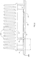
- a classical heat sink as illustrated in Fig. 1 is a thermal conductive device 10, generally in steel or aluminum alloy, principally composed of fins or spikes 12 which present a very important area enabling the heat generated by microprocessor 14 to be dissipated in the ambient air.
- Microprocessor 14 installed on printed circuit board 16 is incorporated in a dielectric case. Dire to this dielectric case, the microprocessor is capacitively coupled with the microprocessor chip. Then, heat sink fins 12 are coupled to the environment thru their parasitic capacitance. Therefore, a part of the electromagnetic energy captured by heat sink 10 due to such a capacitance is re-emitted by fins 12 operating as an antenna.
- the emission of electromagnetic radiation represented by arrows 18 in Fig.1 depends on the size of fins 12 compared with the wavelength of the harmonics generated by microprocessor chip.
- the rule of thumb indicates that fins having a length above one tenth of the wavelength become an antenna. Thus, it is the case with fins having a length of about 10mm which constitute an antenna for the harmonics of 3 GHz and above.
- microprocessor 20 incorporated in a dielectric case is installed on a printed circuit board 22.
- a thermal conductive heat sink 24 principally composed of fins 26 is fixed on the top of microprocessor 20 preferably with a thermal conductive glue. It must be noted that the height of fins 26 and the space therebetween is designed in such a way to provide as much as possible thermal exchange between microprocessor 20 and the ambient air for heat dissipation.
- heat sink 24 is larger than microprocessor 20.
- the latter is encapsulated in a Faraday cage constituted by heat sink 24 on the top and vertical pins such as pins 28, 30 or 32, which are regularly spaced and connected to the ground plane 34 of the printed circuit board 22.
- pins 28, 30 or 32 which are regularly spaced and connected to the ground plane 34 of the printed circuit board 22.
- the number of pins 28, 30 or 32 depend primarily on the highest harmonic wavelength and the rule of thumb is to have spacing L between two pins equal or less than one tenth of the lowest wavelength.
- the spacing L must be less than 1cm.
- An example of implementation with a microprocessor case being 5cm large is a Faraday cage having a side of 8cm and comprising 9 pins such as pins 28, 29 and 30.
- the object of the invention is to provide a radiation blocking device of the Faraday cage type maintaining the electromagnetic emissions inside and being composed of the ground plane, the top constituted by fins or spikes for dissipation the heat and walls preventing the radiation of the smallest wavelengths to be emitted outside.
- the Faraday cage could have solid sidewalls instead of pins, such sidewalls being connected to the ground directly on the top of the printed circuit board or by pinholes, or could be formed by a grid the mesh of which being of a dimension less than the tenth of the smallest wavelength as mentioned above.
- the connection of heat sink 24 to ground plane 34 be a single strap or wire different from pins 28, 30, or 32.
Landscapes
- Cooling Or The Like Of Semiconductors Or Solid State Devices (AREA)
- Cooling Or The Like Of Electrical Apparatus (AREA)
- Shielding Devices Or Components To Electric Or Magnetic Fields (AREA)
Priority Applications (1)
| Application Number | Priority Date | Filing Date | Title |
|---|---|---|---|
| EP98480071A EP0932200A3 (de) | 1998-01-22 | 1998-10-29 | Kühlkörper für Mikroprozessor |
Applications Claiming Priority (3)
| Application Number | Priority Date | Filing Date | Title |
|---|---|---|---|
| EP98480005 | 1998-01-22 | ||
| EP98480005 | 1998-01-22 | ||
| EP98480071A EP0932200A3 (de) | 1998-01-22 | 1998-10-29 | Kühlkörper für Mikroprozessor |
Publications (2)
| Publication Number | Publication Date |
|---|---|
| EP0932200A2 true EP0932200A2 (de) | 1999-07-28 |
| EP0932200A3 EP0932200A3 (de) | 2000-08-23 |
Family
ID=26151813
Family Applications (1)
| Application Number | Title | Priority Date | Filing Date |
|---|---|---|---|
| EP98480071A Withdrawn EP0932200A3 (de) | 1998-01-22 | 1998-10-29 | Kühlkörper für Mikroprozessor |
Country Status (1)
| Country | Link |
|---|---|
| EP (1) | EP0932200A3 (de) |
Cited By (5)
| Publication number | Priority date | Publication date | Assignee | Title |
|---|---|---|---|---|
| WO2008012533A1 (en) * | 2006-07-28 | 2008-01-31 | Iti Scotland Limited | Antenna arrangment as heat sink |
| EP2400545A3 (de) * | 2010-06-23 | 2013-08-28 | Broadcom Corporation | Baugruppe für eine integrierte Schaltung mit Drahtlosfunktion |
| US8901945B2 (en) | 2011-02-23 | 2014-12-02 | Broadcom Corporation | Test board for use with devices having wirelessly enabled functional blocks and method of using same |
| US8928139B2 (en) | 2011-09-30 | 2015-01-06 | Broadcom Corporation | Device having wirelessly enabled functional blocks |
| CN111525228A (zh) * | 2020-05-18 | 2020-08-11 | Oppo广东移动通信有限公司 | 天线模块和电子设备 |
Family Cites Families (6)
| Publication number | Priority date | Publication date | Assignee | Title |
|---|---|---|---|---|
| DE68920195T2 (de) * | 1988-05-06 | 1995-08-03 | Digital Equipment Corp | Schaltungschipspackung zum Schützen gegen elektromagnetische Interferenzen, elektrostatische Entladungen und thermische und mechanische Spannungen. |
| US5650662A (en) * | 1993-08-17 | 1997-07-22 | Edwards; Steven F. | Direct bonded heat spreader |
| US5796170A (en) * | 1996-02-15 | 1998-08-18 | Northern Telecom Limited | Ball grid array (BGA) integrated circuit packages |
| US5713690A (en) * | 1996-05-28 | 1998-02-03 | International Business Machines Corporation | Apparatus for attaching heatsinks |
| GB2324649A (en) * | 1997-04-16 | 1998-10-28 | Ibm | Shielded semiconductor package |
| JP2001523047A (ja) * | 1997-11-10 | 2001-11-20 | パーカー−ハニフイン・コーポレーシヨン | 非導電性熱放散器構成要素 |
-
1998
- 1998-10-29 EP EP98480071A patent/EP0932200A3/de not_active Withdrawn
Cited By (6)
| Publication number | Priority date | Publication date | Assignee | Title |
|---|---|---|---|---|
| WO2008012533A1 (en) * | 2006-07-28 | 2008-01-31 | Iti Scotland Limited | Antenna arrangment as heat sink |
| EP2400545A3 (de) * | 2010-06-23 | 2013-08-28 | Broadcom Corporation | Baugruppe für eine integrierte Schaltung mit Drahtlosfunktion |
| US8901945B2 (en) | 2011-02-23 | 2014-12-02 | Broadcom Corporation | Test board for use with devices having wirelessly enabled functional blocks and method of using same |
| US8928139B2 (en) | 2011-09-30 | 2015-01-06 | Broadcom Corporation | Device having wirelessly enabled functional blocks |
| CN111525228A (zh) * | 2020-05-18 | 2020-08-11 | Oppo广东移动通信有限公司 | 天线模块和电子设备 |
| CN111525228B (zh) * | 2020-05-18 | 2021-08-13 | Oppo广东移动通信有限公司 | 天线模块和电子设备 |
Also Published As
| Publication number | Publication date |
|---|---|
| EP0932200A3 (de) | 2000-08-23 |
Similar Documents
| Publication | Publication Date | Title |
|---|---|---|
| US6912128B2 (en) | Electronics cooling subassembly | |
| KR101116723B1 (ko) | 열소산 플레이트를 포함하는 발광 다이오드 장치 | |
| TW556475B (en) | A cover apparatus for dissipating heat and shielding electromagnetic interference | |
| JPH1197592A (ja) | 熱消散装置 | |
| US20250234493A1 (en) | Apparatus including thermal management mechanism and methods of manufacturing the same | |
| US7616445B2 (en) | Structure and method for efficient thermal dissipation in an electronic assembly | |
| US20080198557A1 (en) | Heat-dissipating module | |
| US20040037042A1 (en) | EMI shielding apparatus | |
| US20080029244A1 (en) | Heat sinks for dissipating a thermal load | |
| EP0932200A2 (de) | Kühlkörper für Mikroprozessor | |
| US6646341B2 (en) | Heat sink apparatus utilizing the heat sink shroud to dissipate heat | |
| CA2456980A1 (en) | Heat removal system | |
| JP3012867B2 (ja) | コンピュ―タ用ヒ―トシンク装置 | |
| KR101360730B1 (ko) | 방열 장치 및 이를 포함하는 전기 장치 | |
| US11240912B2 (en) | Multilayer wiring substrate | |
| CN201222843Y (zh) | 电磁干扰防治模块 | |
| JP4958189B2 (ja) | 集積回路の搭載構造 | |
| JP3008942B1 (ja) | 電子装置の放熱構造 | |
| JPWO2008035540A1 (ja) | 電子装置搭載機器とその共振抑制方法 | |
| US6399877B1 (en) | Heat sink | |
| US9802279B2 (en) | Apparatus and method for a molded plastic fin shell for electronic devices | |
| KR102782628B1 (ko) | 냉각제 순환 유닛을 결합한 pcb 방열 플레이트 | |
| JP2010278113A (ja) | 通信モジュール | |
| US20250311164A1 (en) | Electronic device | |
| CN222424553U (zh) | 电源模块 |
Legal Events
| Date | Code | Title | Description |
|---|---|---|---|
| PUAI | Public reference made under article 153(3) epc to a published international application that has entered the european phase |
Free format text: ORIGINAL CODE: 0009012 |
|
| AK | Designated contracting states |
Kind code of ref document: A2 Designated state(s): DE FR GB |
|
| AX | Request for extension of the european patent |
Free format text: AL;LT;LV;MK;RO;SI |
|
| PUAL | Search report despatched |
Free format text: ORIGINAL CODE: 0009013 |
|
| AK | Designated contracting states |
Kind code of ref document: A3 Designated state(s): AT BE CH CY DE DK ES FI FR GB GR IE IT LI LU MC NL PT SE |
|
| AX | Request for extension of the european patent |
Free format text: AL;LT;LV;MK;RO;SI |
|
| RIC1 | Information provided on ipc code assigned before grant |
Free format text: 7H 01L 23/40 A, 7H 01L 23/60 B, 7H 01L 23/367 B |
|
| 17P | Request for examination filed |
Effective date: 20000918 |
|
| AKX | Designation fees paid |
Free format text: DE FR GB |
|
| STAA | Information on the status of an ep patent application or granted ep patent |
Free format text: STATUS: THE APPLICATION HAS BEEN WITHDRAWN |
|
| 18W | Application withdrawn |
Effective date: 20050810 |