EP0931436B1 - Elektrisches energieverteilungssystem - Google Patents
Elektrisches energieverteilungssystem Download PDFInfo
- Publication number
- EP0931436B1 EP0931436B1 EP97944994A EP97944994A EP0931436B1 EP 0931436 B1 EP0931436 B1 EP 0931436B1 EP 97944994 A EP97944994 A EP 97944994A EP 97944994 A EP97944994 A EP 97944994A EP 0931436 B1 EP0931436 B1 EP 0931436B1
- Authority
- EP
- European Patent Office
- Prior art keywords
- conductors
- arrangement according
- conductor
- load
- distribution line
- Prior art date
- Legal status (The legal status is an assumption and is not a legal conclusion. Google has not performed a legal analysis and makes no representation as to the accuracy of the status listed.)
- Expired - Lifetime
Links
- 239000004020 conductor Substances 0.000 claims description 72
- 239000011888 foil Substances 0.000 claims description 34
- 230000035699 permeability Effects 0.000 claims description 21
- 230000005540 biological transmission Effects 0.000 claims description 20
- 239000012212 insulator Substances 0.000 claims description 9
- 239000000463 material Substances 0.000 claims description 9
- 239000002184 metal Substances 0.000 claims description 8
- 229910052751 metal Inorganic materials 0.000 claims description 8
- 238000004804 winding Methods 0.000 claims description 8
- 239000011810 insulating material Substances 0.000 claims description 7
- 230000005611 electricity Effects 0.000 claims description 2
- -1 polypropylene Polymers 0.000 description 4
- RYGMFSIKBFXOCR-UHFFFAOYSA-N Copper Chemical compound [Cu] RYGMFSIKBFXOCR-UHFFFAOYSA-N 0.000 description 3
- 229910052802 copper Inorganic materials 0.000 description 3
- 239000010949 copper Substances 0.000 description 3
- 230000004907 flux Effects 0.000 description 3
- 229920000265 Polyparaphenylene Polymers 0.000 description 2
- 239000004743 Polypropylene Substances 0.000 description 2
- UCKMPCXJQFINFW-UHFFFAOYSA-N Sulphide Chemical compound [S-2] UCKMPCXJQFINFW-UHFFFAOYSA-N 0.000 description 2
- 239000000853 adhesive Substances 0.000 description 2
- 230000001070 adhesive effect Effects 0.000 description 2
- 230000000694 effects Effects 0.000 description 2
- 239000004033 plastic Substances 0.000 description 2
- 229920000728 polyester Polymers 0.000 description 2
- 229920001155 polypropylene Polymers 0.000 description 2
- 229910000851 Alloy steel Inorganic materials 0.000 description 1
- 229910000531 Co alloy Inorganic materials 0.000 description 1
- 229910000881 Cu alloy Inorganic materials 0.000 description 1
- 229910000831 Steel Inorganic materials 0.000 description 1
- 239000003522 acrylic cement Substances 0.000 description 1
- 239000010941 cobalt Substances 0.000 description 1
- GUTLYIVDDKVIGB-UHFFFAOYSA-N cobalt atom Chemical compound [Co] GUTLYIVDDKVIGB-UHFFFAOYSA-N 0.000 description 1
- 238000001816 cooling Methods 0.000 description 1
- 238000010586 diagram Methods 0.000 description 1
- 230000005684 electric field Effects 0.000 description 1
- 238000010791 quenching Methods 0.000 description 1
- 230000000171 quenching effect Effects 0.000 description 1
- 238000012216 screening Methods 0.000 description 1
- 239000010959 steel Substances 0.000 description 1
Images

Classifications
-
- H—ELECTRICITY
- H01—ELECTRIC ELEMENTS
- H01B—CABLES; CONDUCTORS; INSULATORS; SELECTION OF MATERIALS FOR THEIR CONDUCTIVE, INSULATING OR DIELECTRIC PROPERTIES
- H01B7/00—Insulated conductors or cables characterised by their form
- H01B7/0009—Details relating to the conductive cores
- H01B7/0018—Strip or foil conductors
-
- H—ELECTRICITY
- H05—ELECTRIC TECHNIQUES NOT OTHERWISE PROVIDED FOR
- H05B—ELECTRIC HEATING; ELECTRIC LIGHT SOURCES NOT OTHERWISE PROVIDED FOR; CIRCUIT ARRANGEMENTS FOR ELECTRIC LIGHT SOURCES, IN GENERAL
- H05B39/00—Circuit arrangements or apparatus for operating incandescent light sources
-
- H—ELECTRICITY
- H05—ELECTRIC TECHNIQUES NOT OTHERWISE PROVIDED FOR
- H05B—ELECTRIC HEATING; ELECTRIC LIGHT SOURCES NOT OTHERWISE PROVIDED FOR; CIRCUIT ARRANGEMENTS FOR ELECTRIC LIGHT SOURCES, IN GENERAL
- H05B41/00—Circuit arrangements or apparatus for igniting or operating discharge lamps
- H05B41/14—Circuit arrangements
- H05B41/24—Circuit arrangements in which the lamp is fed by high frequency ac, or with separate oscillator frequency
- H05B41/245—Circuit arrangements in which the lamp is fed by high frequency ac, or with separate oscillator frequency for a plurality of lamps
Definitions
- THE PRESENT INVENTION relates to a power distribution system, and more particularly relates to a power distribution system adapted to distribute electric power from a power source to at least one load.
- the power may be distributed at a typical "mains" voltage of 240 volts (or, in some countries 110 volts) and at a typical "mains" frequency of 50 cycles per second (in some countries, 60 cycles per second).
- a disadvantage of this type of distribution system is that since a relatively low voltage is used, for a moderate power supply, a substantial current flows, meaning that the conductors must be capable of carrying a substantial current. Consequently, the cables typically include conductors formed of copper, the conductors having a relatively large cross-section.
- a distribution system of this type is utilised with a discharge lamp, for example, a step-up transformer has to be utilised. Since the frequency of the alternating current is relatively low, the transformer must be relatively bulky.
- An electronic ballast is small and light and also, in connection with a discharge lamp, provides high efficiency and a light that is substantially flicker-free.
- an electronic ballast there is a need for a high frequency alternating current.
- a power factor corrector must be provided to ensure that the power factor is "sen" at the main supply is appropriate.
- EP-A-0397080 discloses a flat screened electrical cable comprising four flat conductors arranged parallel to each other in a single plain, with one of the conductors being broader than the rest and having a facing contact with a metal foil surrounding all the conductors and screening the arrangement.
- EP-A-0209826 discloses an electrical cable.
- the conductors comprise multi-core conductors contained within a complex sheath arrangement which includes a layers of high relative permeability which surrounds all of the conductors.
- the present invention seeks to provide an improved power distribution system.
- an electric power distribution arrangement comprising a source of alternating current having a frequency of 10 kHz or greater, a distribution line connected to said source, the distribution line comprising three layers constituted by two conductors, each of substantially flat configuration, the conductors being located in spaced parallelism and being located a short distance apart, and an insulator that separates the two conductors, at least one of the conductors included in the three layers of the transmission line being associated with a respective further element formed of a material of high relative permeability, that element comprising a foil secured to the face of the conductor remote from the insulator, the arrangement further comprising at least one load connected to said conductors to receive electric power therefrom.
- the load is connected directly to the two conductors.
- the load is connected to the conductors by means of a transformer, the transformer having a primary winding connected to the two conductors, and having a secondary winding connected to the load.
- the load comprises a low voltage incandescent lamp, but preferably the load comprises a discharge lamp, an impedance being provided which is connected in circuit with the secondary winding and the discharge lamp.
- the or each load comprises a discharge lamp connected to one conductor of the distribution line by means of an inductance and connected directly to the other conductor of the distribution line.
- the source of alternating current comprises a power factor corrector which receives supply from a mains electricity supply, and an inverter which receives power from the power factor corrector.
- the power factor corrector comprises a rectifier producing a DC output, the DC output of the power factor corrector being provided as an input to the inverter.
- a transformer is provided located between the source of high frequency current and the distribution line.
- a second element of high permeability is provided associated with the other conductor, that second element comprising a foil secured to the face of the conductor remote from the insulator.
- each element of high relative permeability extends laterally beyond the associated flat conductor.
- the or each element of high permeability is formed of a amorphous or nano-crystalline metal, the insulator separating the conductors comprising a sheet of insulating material.
- the foil is separated from the face of the conductor to which it is secured by means of an insulating layer.
- a power transmission line which is suitable for use in transmitting power of a voltage between, for example, 150 volts and 1 kv, at an operating frequency of greater than 10 kHz, most preferably at a frequency of 60 kHz.
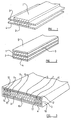
- the power transmission line comprises two principal conductors 1, 2.
- Each of the conductors is of substantially flat or rectangular cross-section, with two opposed parallel flat faces.
- the conductors may be formed of copper or copper alloy and may have a thickness of between 0.025 and 0.25 mm, and a width of up to 30 mm, depending upon the current to be carried.
- the two conductors are separated by a sheet of insulating material 3.
- the insulating material may be an appropriate plastic such as a polyester, polypropylene or polyphenylene sulphide.
- the thickness of the insulating sheet 3 depends upon the voltage to be carried by the conductors 1 and 2 and may typically be of the order of 0.1 millimetres.
- the insulating sheet 3, in the embodiment illustrated in Figure 1, has such a width that it extends beyond the conductors 1 and 2.
- a foil 4 is associated with the conductor 2.
- the foil 4 is made of a material having a high relative permeability. Typically the relative permeability of the foil may be of the order of 10 5 .
- the foil 4 is secured to the face of the conductive element 2 which is remote from the insulating layer 3.
- the foil 4 has a width which is greater than the width of the conductive element 2, so that parts of the foil project beyond the conductive element 2 on each side thereof.
- the foil 4 may be formed from an amorphous or nano-crystalline metal, such as steel or a cobalt/steel alloy. Such a metal has a high resistivity.
- a foil of high permeability of this type may be created by quenching cooling molten metal at a very high speed, for example, at a speed of 10 6 degrees celsius per second.
- the molten metal may be sprayed to a cooled, rapidly rotating drum. The metal cools on the drum and may be removed from the drum in the form of a strip.
- the foil 4 of high relative permeability constitutes a low reluctance path for magnetic field and, when a distribution line, as illustrated in Figure 1 is utilised, on the side of the transmission line where the foil is provided there is a 100 fold reduction in the flux that causes the radio frequency interference, (as compared with an equivalent transmission line without a foil of relatively high permeability) and on the other side of the transmission line there is a ten fold reduction in the flux.
- the embodiment of Figure 1 may be altered by providing a second foil corresponding to the foil 4, the second foil being secured to the exposed face of conductor 1.
- Figure 2 illustrates a second embodiment of the invention in which the conductors 1 and 2 are as described above, with the insulating layer 3 being of the same width as that of the conductors 1 and 2.
- a foil 4 of high permeability material is provided in contact with the conductor 2, but has the same width as the width of the conductor 2.
- a second foil 5, of high permeability material, which corresponds directly with foil 4, is connected to the conductor 1.
- the flux that generates the radio frequency interference signal is reduced, on each side of the distribution line, of a factor of approximately 1,000.
- the foils have the same width as the width of the conductors. This provides a transmission line which is easy to handle, and which, if desired, may be easily provided with an insulating sheath.
- the shielding effect provided by the foils 4 and 5 is not as great as it would be if the foils 4 and 5 were wider than the conductors 1,2.
- Figure 3 illustrates a further embodiment of a transmission line.
- the copper conductor 1 is provided with a central core region 10 which extends axially of the transmission line and, on either side thereof, two further spaced apart regions 11,12, which extend in parallelism with the core region 10.
- the conductor 3 comprises a central core region 13 and, on either side, two further spaced apart regions 14,15.
- the conductors 1 and 2 are separated by an insulating layer 3.
- the conductor 1 is separated from a foil 5 of high permeability by a thin insulating layer 16.
- the conductor 2 is separated from the foil 4 by means of a thin insulating layer 17.
- the spaces between the various parts of each conductor 1 and 2 may be filled with an adhesive such as an acrylic adhesive.
- an outer sleeve 18 of an appropriate insulating material such as a plastic material.
- the layers of foil of high permeability material are separated from the conductive layers with which they are associated by means of a respective thin layer of an insulating material.
- each conductive layer is formed of a central core and further components which extend parallel with that core but spaced therefrom.
- the provision of an arrangement of this type has been found to reduce eddycurrents which might otherwise occur at the edge of a relatively large flat conductive core.
- the provision of an adhesive between the various components of the conductive element help ensure that the various layers that form the laminate that constitutes the distribution line illustrated in Figure 3, remain in a predetermined position relative to each other.
- distribution lines of the type described above provide very low inductance, low resistance and high capacitance.
- the capacitance provided by the distribution line can be incorporated into the circuit of the power generator which is utilised as a supply power through the distribution line, for example as part of a resonating circuit.
- an appropriate insulating material for the insulating sheet 3 between the conductors 1 and 2 so that the capacitance is of a high quality, that is to say with a low power loss.
- the polyester material mentioned above provides good characteristics and is suitable for use at a low to medium temperature.
- Polypropylene provides better characteristics, but is only suitable for use at low temperatures.
- Polyphenylene sulphide provides good properties, and is suitable for use at high to medium temperatures.
- a mains supply 20 is connected to a power factor corrector 21.
- the power factor corrector is intended to ensure that the power factor of the current drawn by the load is appropriate.
- the power factor corrector is a rectifier which produces a 340 volt DC output.
- the output of the power factor corrector 21 is provided to a high frequency inverter 22.
- the output of the high frequency inverter 22 is typically 10 kHz or greater.
- the preferred frequency is 60 kHz.
- the output of the inverter 22 is connected to a transformer 23 which must be considered to be "optional".
- the transformer 23 may provide an isolating function, separating, electrically, the components now to be described from the components described above.
- the transformer may step the output voltage, provided by the inverter 22, either up or down, as is desired.
- the output of the transformer 23 is connected to a transmission line 24.
- the transmission line 24 may have the form as illustrated, for example, in Figure 1, or Figure 2 or Figure 3 and as described above.
- the two conductors 1,2 of the power distribution line 24 may be connected, as illustrated, directly to a load 25.
- the load 25 may comprise an appropriate incandescent lamp, or could comprise a heater or some other equivalent device.
- a transformer 26 may have a primary winding connected to the two conductors of the distribution line 24.
- the secondary winding of the transformer may be connected to a load 27. Because the alternating current present on the distribution line 24 has a high frequency, in excess of 10 kHz, the transformer need physically only be very small.
- the load may comprise, for example, a 12 volt dichroic incandescent lamp or, alternatively, a discharge lamp. Of course, in the case of a discharge lamp, an appropriate impedance, such as an inductance, will need to be incorporated within the circuit to act as a ballast.
- one conductor of the distribution line 24 may be connected by means of an inductor 28 to a load 29, the other conductor in the distribution line 24 being connected directly to the load.
- the load may comprise a discharge lamp.
- the inductor 28 provides an appropriate ballasting effect.
- FIG. 5 illustrates a transmission line 3 of the types shown in Figure 2.
- a clip 22 is provided which has two spaced apart blades 33,34, which engages the opposed faces of the transmission line.
- the high permeability foils 4 and 5 are amorphous and thus have a high resistance, nevertheless, since the blades 33,34 of the clip 25 engage a substantial area of the foils 4 and 5, the arms of the clip may provide an appropriate power-take-off.
- the arms of the clip may be connected to, for example, a housing 35 which contains an appropriate transformer to an item which is to be supplied with electrical power.
- a clip as shown may establish the content between a load and a distribution line.
- the electric power is distributed at a high frequency.
- problems that might arise, in connection with the use of a high frequency distribution system, as a consequence of "interference" are overcome by the use of the specific transmission line which incorporates two substantially flat conductors which are located in spaced parallelism, very close to each other, and which are separated by an appropriate insulator.
- the problem of interference may be reduced further by providing the high permeability material mentioned above.
- the power may be distributed at a moderate voltage, for example, 300-340 RMS, or 150-170 RMS or approximately 85 RMS. If the power is distributed at a moderate voltage and needs to be transformed to a lower or higher voltage at the point of utilisation only a physically small transformer need be utilised, because of, the high frequency.
- a moderate voltage for example, 300-340 RMS, or 150-170 RMS or approximately 85 RMS.
- a mains supply 20 through an appropriate power factor corrector 21 to a high frequency distribution system, with a plurality of lamps being connected to the distribution system, each lamp being associated with its own electronic ballast. Because the lamps are provided with high frequency alternating current, ballasts need only be small and light and if the lamps are discharge lamps, it is possible to obtain high efficiency and substantially flicker-free-light.
- the power factor corrector satisfies the appropriate legislation, and because a distribution line of the type described with reference to Figures 1, 2 or 3 is utilised, there is virtually no H-field interference.
- a main supply is connected through a power factor corrector to a high frequency inverter to generate the initial high frequency.
- the high frequency may be generated directly from the mains using an appropriate frequency generator.
Landscapes
- Circuit Arrangements For Discharge Lamps (AREA)
- Ac-Ac Conversion (AREA)
- Coils Of Transformers For General Uses (AREA)
- Inverter Devices (AREA)
- Patch Boards (AREA)
Claims (14)
- Elektrische Energieverteilungsvorrichtung, die eine Quelle (20) für einen Wechselstrom, der eine Frequenz von 10 kHz oder höher aufweist, eine Verteilungsleitung, die mit der Quelle verbunden ist, wobei die Verteilungsleitung drei Schichten umfaßt, die von zwei Leitern (12) gebildet werden, von denen jeder eine im wesentlichen flache Konfiguration aufweist, wobei die Leiter in Parallelität mit Abstand angeordnet sind und mit einem kleinen Abstand voneinander getrennt angeordnet sind, und einen Isolator (3) umfaßt, der die zwei Leiter voneinander trennt, wobei wenigstens einer der Leiter (1), der in den drei Schichten der Verteilungsleitung enthalten ist, einem entsprechenden weiteren Element (5) zugeordnet ist, das aus einem Material mit einer hohen relativen Permeabilität hergestellt ist, wobei das Element (5) eine Folie umfaßt, die an der Oberfläche des Leiters (1), von dem Isolator (3) entfernt, sicher befestigt ist, wobei die Vorrichtung ferner wenigstens eine Last (25, 27, 29) umfaßt, die mit den Leitern verbunden ist, um von diesen mit elektrischer Energie versorgt zu werden.
- Vorrichtung nach Anspruch 1, wobei die Last (25, 27, 29) direkt mit den zwei Leitern (1, 2) verbunden ist.
- Vorrichtung nach Anspruch 1, wobei die Last (27) mittels eines Transformators (26) mit den Leitern (1, 2) verbunden ist, wobei der Transformator eine Primärwicklung aufweist, die mit den zwei Leitern verbunden ist, und eine Sekundärwicklung aufweist, die mit der Last verbunden ist.
- Vorrichtung nach Anspruch 3, wobei die Last (27) eine Niederspannungsglühlampe umfaßt.
- Vorrichtung nach Anspruch 3, wobei die Last (29) eine Entladungslampe umfaßt, wobei eine Impedanz zur Verfügung gestellt wird, die mit der Sekundärwicklung und der Entladungslampe in einem Schaltkreis verbunden ist.
- Vorrichtung nach Anspruch 1, wobei die oder jede Last eine Entladungslampe (29) umfaßt, die mit einem Leiter (1) der Verteilungsleitung mittels einer Induktivität (28) verbunden ist und direkt mit dem anderen Leiter (2) der Verteilungsleitung verbunden ist.
- Vorrichtung nach einem der vorhergehenden Ansprüche, wobei die Wechselstromquelle eine Leistungsfaktorkorrekturvorrichtung (21), die von einer Hauptelektrizitätsversorgung gespeist wird, und einen Wechselrichter (22) umfaßt, der von der Leistungsfaktorkorrekturvorrichtung mit Energie versorgt wird.
- Vorrichtung nach Anspruch 7, wobei die Leistungsfaktorkorrekturvorrichtung (21) einen Gleichrichter umfaßt, der eine DC-Ausgangsleistung zur Verfügung stellt, wobei die DC-Ausgangsleistung der Leistungsfaktorkorrekturvorrichtung als eine Eingangsleistung für den Wechselrichter bereit gestellt wird.
- Vorrichtung nach einem der vorhergehenden Ansprüche, wobei ein Transformator (23) zur Verfügung gestellt wird, der zwischen der Quelle des Hochfrequenzstroms und der Verteilungsleitung angeordnet ist.
- Vorrichtung nach einem der vorhergehenden Ansprüche, wobei ein zweites Element (4) einer hohen Permeabilität zur Verfügung gestellt wird, welches dem anderen Leiter (2) zugeordnet ist, wobei das zweite Element eine Folie umfaßt, die an der Oberfläche des Leiters, von dem Isolator (3) entfernt, sicher befestigt ist.
- Vorrichtung nach einem der vorhergehenden Ansprüche, wobei sich das oder jedes Element (3, 4) mit einer hohen relativen Permeabilität seitlich über den zugeordneten flachen Leiter (1, 2) erstreckt.
- Vorrichtung nach einem der vorhergehenden Ansprüche, wobei das oder jedes Element (4, 5) mit einer hohen Permeabilität aus einem amorphen oder nanokristallinen Metall gebildet ist.
- Vorrichtung nach einem der vorhergehenden Ansprüche, wobei der Isolator (3), der die Leiter trennt, eine Schicht eines isolierenden Materials umfaßt.
- Vorrichtung nach einem der vorhergehenden Ansprüche, wobei die oder jede Folie (4, 5) von der Oberfläche des Leiters separiert ist, an dem sie mittels einer isolierenden Schicht (16, 17) sicher befestigt ist.
Applications Claiming Priority (3)
| Application Number | Priority Date | Filing Date | Title |
|---|---|---|---|
| GBGB9621353.3A GB9621353D0 (en) | 1996-10-11 | 1996-10-11 | Improvements in or relating to a power distribution system |
| GB9621353 | 1996-10-11 | ||
| PCT/GB1997/002799 WO1998017085A1 (en) | 1996-10-11 | 1997-10-10 | A power distribution system |
Publications (2)
| Publication Number | Publication Date |
|---|---|
| EP0931436A1 EP0931436A1 (de) | 1999-07-28 |
| EP0931436B1 true EP0931436B1 (de) | 2002-01-16 |
Family
ID=10801363
Family Applications (1)
| Application Number | Title | Priority Date | Filing Date |
|---|---|---|---|
| EP97944994A Expired - Lifetime EP0931436B1 (de) | 1996-10-11 | 1997-10-10 | Elektrisches energieverteilungssystem |
Country Status (9)
| Country | Link |
|---|---|
| US (1) | US6320133B1 (de) |
| EP (1) | EP0931436B1 (de) |
| JP (1) | JP2001505707A (de) |
| DE (1) | DE69709669T2 (de) |
| DK (1) | DK0931436T3 (de) |
| ES (1) | ES2173492T3 (de) |
| GB (1) | GB9621353D0 (de) |
| PT (1) | PT931436E (de) |
| WO (1) | WO1998017085A1 (de) |
Families Citing this family (16)
| Publication number | Priority date | Publication date | Assignee | Title |
|---|---|---|---|---|
| EP1244337A1 (de) * | 2001-03-20 | 2002-09-25 | MAGNETEK S.p.A. | Beleuchtungsanordnung mit Stromleiterschiene und mehreren Beleuchtungskörpern |
| DE10124086B4 (de) * | 2001-05-16 | 2013-11-07 | Schott Ag | Elektrisches Gerät mit einer transparenten Stromzuführung |
| JP3876770B2 (ja) * | 2002-06-07 | 2007-02-07 | 日産自動車株式会社 | 配線構造 |
| GB0305228D0 (en) * | 2003-03-07 | 2003-04-09 | Hewlett Packard Development Co | A flat flexible cable |
| US7145073B2 (en) * | 2003-09-05 | 2006-12-05 | Southwire Company | Electrical wire and method of fabricating the electrical wire |
| US7737359B2 (en) * | 2003-09-05 | 2010-06-15 | Newire Inc. | Electrical wire and method of fabricating the electrical wire |
| US7217884B2 (en) | 2004-03-02 | 2007-05-15 | Southwire Company | Electrical wire and method of fabricating the electrical wire |
| US8237051B2 (en) * | 2003-09-05 | 2012-08-07 | Newire, Inc. | Flat wire extension cords and extension cord devices |
| US7038400B2 (en) * | 2004-03-12 | 2006-05-02 | Juno Manufacturing, Inc. | Constant current Class 3 lighting system |
| JP2007193999A (ja) * | 2006-01-17 | 2007-08-02 | Sony Chemical & Information Device Corp | 伝送ケーブル |
| DE102007063675B4 (de) * | 2007-06-13 | 2017-04-06 | Auto-Kabel Management Gmbh | Kraftfahrzeugenergiekabel |
| CN101965757A (zh) * | 2007-10-01 | 2011-02-02 | 皇家飞利浦电子股份有限公司 | 高压电连接线 |
| KR101373850B1 (ko) | 2014-02-07 | 2014-03-26 | 주식회사 네스앤텍 | 유선 비행체의 전원공급시스템 |
| DE102017116444A1 (de) * | 2017-07-20 | 2018-10-25 | Lisa Dräxlmaier GmbH | Elektrische Flachleiteranordnung für ein Fahrzeug |
| DE102017116446A1 (de) * | 2017-07-20 | 2018-10-25 | Lisa Dräxlmaier GmbH | Elektrische Flachleiteranordnung für ein Fahrzeug |
| JP2019096546A (ja) * | 2017-11-27 | 2019-06-20 | トヨタ自動車株式会社 | 平型配線構造 |
Family Cites Families (34)
| Publication number | Priority date | Publication date | Assignee | Title |
|---|---|---|---|---|
| US2060913A (en) | 1934-07-07 | 1936-11-17 | Western Electric Co | Electrical conductor |
| FR1428517A (fr) | 1964-11-26 | 1966-02-18 | Organes de transmission d'énergie électrique à absorption sélective | |
| AT262440B (de) * | 1965-10-16 | 1968-06-10 | Siemens Ag | Bandförmiger Supraleiter |
| US3671675A (en) | 1969-06-17 | 1972-06-20 | Thomas I Ress | High-frequency communication system |
| US3973227A (en) * | 1972-06-15 | 1976-08-03 | Societa Italiana Telecomunicazioni Siemens S.P.A. | Transmission line for TDM communication system |
| FR2334182A1 (fr) * | 1975-12-03 | 1977-07-01 | Furukawa Electric Co Ltd | Cable comportant un compose supraconducteur et procede de fabrication d'un tel cable |
| US4204273A (en) * | 1977-01-31 | 1980-05-20 | Goldberg Gerald M | Construction of illuminating ribbon of light bulbs |
| US4109307A (en) | 1977-05-04 | 1978-08-22 | Gte Sylvania Incorporated | High power factor conversion circuitry |
| BE886846Q (fr) * | 1977-11-29 | 1981-04-16 | Mayer Ferdy | Fil ou cable antiparasite pour haute frequence |
| FR2437686A1 (fr) * | 1978-09-29 | 1980-04-25 | Mayer Ferdy | Element electrique a pertes, tel que fil, cable et ecran, resistant et absorbant |
| US4694123A (en) * | 1982-01-13 | 1987-09-15 | Elxsi | Backplane power connector system |
| JPS58143509A (ja) * | 1982-02-22 | 1983-08-26 | Toshiba Corp | 変圧器 |
| US4651059A (en) * | 1984-01-09 | 1987-03-17 | Nilssen Ole K | High-frequency power-limited lighting system |
| US4540224A (en) | 1983-08-23 | 1985-09-10 | Cooper Industries, Inc. | Grounding clip for use with shielded, jacketed flat cable |
| US4717357A (en) * | 1984-07-13 | 1988-01-05 | Thomas & Betts Corporation | System and method for electrical power installation |
| GB8424285D0 (en) * | 1984-09-26 | 1984-10-31 | Allied Corp | Electric cables |
| DE3620595A1 (de) * | 1985-07-26 | 1987-02-05 | Mitec Moderne Ind Gmbh | Kabel |
| JPS6338541A (ja) | 1986-08-01 | 1988-02-19 | Nippon Mining Co Ltd | インジウムの精製方法 |
| US4894124A (en) | 1988-02-16 | 1990-01-16 | Polyonics Corporation | Thermally stable dual metal coated laminate products made from textured polyimide film |
| US4864081A (en) * | 1988-05-03 | 1989-09-05 | Amp Incorporated | Insulative covering for undercarpet power cable splice |
| US4845311A (en) * | 1988-07-21 | 1989-07-04 | Hughes Aircraft Company | Flexible coaxial cable apparatus and method |
| US5003227A (en) * | 1988-08-15 | 1991-03-26 | Nilssen Ole K | Power distribution for lighting systems |
| FR2646956A1 (fr) * | 1989-05-12 | 1990-11-16 | Filotex Sa | Cable electrique plat blinde a pluralite de conducteurs paralleles |
| JPH0743867Y2 (ja) | 1989-07-05 | 1995-10-09 | 動力炉・核燃料開発事業団 | 給電用ブスバー |
| US5172310A (en) | 1991-07-10 | 1992-12-15 | U.S. Windpower, Inc. | Low impedance bus for power electronics |
| JP3241139B2 (ja) * | 1993-02-04 | 2001-12-25 | 三菱電機株式会社 | フィルムキャリア信号伝送線路 |
| US5393933A (en) * | 1993-03-15 | 1995-02-28 | Goertz; Ole S. | Characteristic impedance corrected audio signal cable |
| JPH07169343A (ja) * | 1993-10-21 | 1995-07-04 | Sumitomo Electric Ind Ltd | 超電導ケーブル導体 |
| US5510974A (en) | 1993-12-28 | 1996-04-23 | Philips Electronics North America Corporation | High frequency push-pull converter with input power factor correction |
| JPH11506865A (ja) * | 1995-06-05 | 1999-06-15 | セクストン、ロバート・ジェイ | 平形の表面取り付け式多目的電線 |
| US5847324A (en) * | 1996-04-01 | 1998-12-08 | International Business Machines Corporation | High performance electrical cable |
| US5801124A (en) * | 1996-08-30 | 1998-09-01 | American Superconductor Corporation | Laminated superconducting ceramic composite conductors |
| GB9621352D0 (en) | 1996-10-11 | 1996-12-04 | Tunewell Technology Ltd | Improvements in or relating to a power distribution line |
| US6005193A (en) * | 1997-08-20 | 1999-12-21 | Markel; Mark L. | Cable for transmitting electrical impulses |
-
1996
- 1996-10-11 GB GBGB9621353.3A patent/GB9621353D0/en active Pending
-
1997
- 1997-10-10 DE DE69709669T patent/DE69709669T2/de not_active Expired - Fee Related
- 1997-10-10 DK DK97944994T patent/DK0931436T3/da active
- 1997-10-10 PT PT97944994T patent/PT931436E/pt unknown
- 1997-10-10 EP EP97944994A patent/EP0931436B1/de not_active Expired - Lifetime
- 1997-10-10 US US09/284,331 patent/US6320133B1/en not_active Expired - Fee Related
- 1997-10-10 WO PCT/GB1997/002799 patent/WO1998017085A1/en active IP Right Grant
- 1997-10-10 ES ES97944994T patent/ES2173492T3/es not_active Expired - Lifetime
- 1997-10-10 JP JP51809998A patent/JP2001505707A/ja not_active Ceased
Also Published As
| Publication number | Publication date |
|---|---|
| DE69709669T2 (de) | 2003-08-28 |
| DK0931436T3 (da) | 2002-05-06 |
| GB9621353D0 (en) | 1996-12-04 |
| JP2001505707A (ja) | 2001-04-24 |
| EP0931436A1 (de) | 1999-07-28 |
| DE69709669D1 (de) | 2002-02-21 |
| PT931436E (pt) | 2002-07-31 |
| ES2173492T3 (es) | 2002-10-16 |
| US6320133B1 (en) | 2001-11-20 |
| WO1998017085A1 (en) | 1998-04-23 |
Similar Documents
| Publication | Publication Date | Title |
|---|---|---|
| EP0931436B1 (de) | Elektrisches energieverteilungssystem | |
| CA2000467C (en) | High-frequency heating apparatus using frequency-converter-type power supply | |
| WO2020238192A1 (zh) | 线圈绕组、线圈模组、发射装置、接收装置、系统和终端 | |
| US7646279B2 (en) | Apparatus for supplying energy to a load and a related system | |
| TWI584310B (zh) | 用於環形磁芯電磁元件之屏蔽與利用此屏蔽之環形磁芯電磁元件 | |
| ES2098087T3 (es) | Un aparato para sellar material de envasado recubierto de termoplastico. | |
| EP0931373A1 (de) | Ein energieverteilungsleitung | |
| AU1965399A (en) | Transformer | |
| RU2388092C2 (ru) | Импульсный трансформатор с фольговой обмоткой | |
| US5631815A (en) | High voltage power supply | |
| EP0336771A2 (de) | Integrierter Kondensator und Spulen/Transformatoren mit isoliertem, amorphem Metallband | |
| CN1298189A (zh) | 小型磁装置的电磁干扰屏蔽 | |
| EP0934594A1 (de) | Drosselspule | |
| EP1057193A2 (de) | Herstellungsverfahren eines supraleiter-mehrphasenkabels mit n phasen | |
| CO4810271A1 (es) | Metodo y disposicion para regular un transformador reactor, y un transformador/reactor | |
| KR880701061A (ko) | 이온전도 램프용 개량 밸러스트 | |
| WO1998043259A1 (en) | An arrangement at a conductor on high voltage potential | |
| KR20060037366A (ko) | 냉각 장치를 구비한 유도 소자 및 상기 유도 소자의 용도 | |
| US5489825A (en) | Transformer | |
| GB2066559A (en) | Fluorescent lamp with reduced electromagnetic interference | |
| JP2002050538A (ja) | コンデンサ | |
| JP2918521B2 (ja) | 電子レンジ用電源供給装置に適用される高圧ヒューズ | |
| US20040174145A1 (en) | Transformer/rectifier arrangement | |
| CN113579450B (zh) | 一种电磁焊接结构 | |
| KR101906483B1 (ko) | 복합식 자가 전원 공급이 가능한 부스바 상태 감지장치 및 이를 이용한 배전반 감시 시스템 |
Legal Events
| Date | Code | Title | Description |
|---|---|---|---|
| PUAI | Public reference made under article 153(3) epc to a published international application that has entered the european phase |
Free format text: ORIGINAL CODE: 0009012 |
|
| 17P | Request for examination filed |
Effective date: 19990429 |
|
| AK | Designated contracting states |
Kind code of ref document: A1 Designated state(s): BE DE DK ES FR GB IT NL PT SE |
|
| 17Q | First examination report despatched |
Effective date: 19990813 |
|
| GRAG | Despatch of communication of intention to grant |
Free format text: ORIGINAL CODE: EPIDOS AGRA |
|
| GRAG | Despatch of communication of intention to grant |
Free format text: ORIGINAL CODE: EPIDOS AGRA |
|
| GRAH | Despatch of communication of intention to grant a patent |
Free format text: ORIGINAL CODE: EPIDOS IGRA |
|
| GRAH | Despatch of communication of intention to grant a patent |
Free format text: ORIGINAL CODE: EPIDOS IGRA |
|
| GRAA | (expected) grant |
Free format text: ORIGINAL CODE: 0009210 |
|
| REG | Reference to a national code |
Ref country code: GB Ref legal event code: IF02 |
|
| AK | Designated contracting states |
Kind code of ref document: B1 Designated state(s): BE DE DK ES FR GB IT NL PT SE |
|
| REF | Corresponds to: |
Ref document number: 69709669 Country of ref document: DE Date of ref document: 20020221 |
|
| REG | Reference to a national code |
Ref country code: DK Ref legal event code: T3 |
|
| ET | Fr: translation filed | ||
| REG | Reference to a national code |
Ref country code: PT Ref legal event code: SC4A Free format text: AVAILABILITY OF NATIONAL TRANSLATION Effective date: 20020415 |
|
| REG | Reference to a national code |
Ref country code: ES Ref legal event code: FG2A Ref document number: 2173492 Country of ref document: ES Kind code of ref document: T3 |
|
| PLBE | No opposition filed within time limit |
Free format text: ORIGINAL CODE: 0009261 |
|
| STAA | Information on the status of an ep patent application or granted ep patent |
Free format text: STATUS: NO OPPOSITION FILED WITHIN TIME LIMIT |
|
| 26N | No opposition filed | ||
| PGFP | Annual fee paid to national office [announced via postgrant information from national office to epo] |
Ref country code: DK Payment date: 20030328 Year of fee payment: 6 Ref country code: BE Payment date: 20030328 Year of fee payment: 6 Ref country code: SE Payment date: 20030328 Year of fee payment: 6 Ref country code: GB Payment date: 20030328 Year of fee payment: 6 |
|
| PGFP | Annual fee paid to national office [announced via postgrant information from national office to epo] |
Ref country code: NL Payment date: 20030331 Year of fee payment: 6 Ref country code: FR Payment date: 20030331 Year of fee payment: 6 |
|
| PGFP | Annual fee paid to national office [announced via postgrant information from national office to epo] |
Ref country code: PT Payment date: 20030421 Year of fee payment: 6 |
|
| PGFP | Annual fee paid to national office [announced via postgrant information from national office to epo] |
Ref country code: ES Payment date: 20030429 Year of fee payment: 6 |
|
| PG25 | Lapsed in a contracting state [announced via postgrant information from national office to epo] |
Ref country code: GB Free format text: LAPSE BECAUSE OF NON-PAYMENT OF DUE FEES Effective date: 20031010 |
|
| PG25 | Lapsed in a contracting state [announced via postgrant information from national office to epo] |
Ref country code: SE Free format text: LAPSE BECAUSE OF NON-PAYMENT OF DUE FEES Effective date: 20031011 Ref country code: ES Free format text: LAPSE BECAUSE OF NON-PAYMENT OF DUE FEES Effective date: 20031011 |
|
| PG25 | Lapsed in a contracting state [announced via postgrant information from national office to epo] |
Ref country code: DK Free format text: LAPSE BECAUSE OF NON-PAYMENT OF DUE FEES Effective date: 20031031 Ref country code: BE Free format text: LAPSE BECAUSE OF NON-PAYMENT OF DUE FEES Effective date: 20031031 |
|
| BERE | Be: lapsed |
Owner name: *TUNEWELL TECHNOLOGY LTD Effective date: 20031031 |
|
| PG25 | Lapsed in a contracting state [announced via postgrant information from national office to epo] |
Ref country code: PT Free format text: LAPSE BECAUSE OF NON-PAYMENT OF DUE FEES Effective date: 20040430 |
|
| PG25 | Lapsed in a contracting state [announced via postgrant information from national office to epo] |
Ref country code: NL Free format text: LAPSE BECAUSE OF NON-PAYMENT OF DUE FEES Effective date: 20040501 |
|
| EUG | Se: european patent has lapsed | ||
| GBPC | Gb: european patent ceased through non-payment of renewal fee |
Effective date: 20031010 |
|
| REG | Reference to a national code |
Ref country code: DK Ref legal event code: EBP |
|
| PG25 | Lapsed in a contracting state [announced via postgrant information from national office to epo] |
Ref country code: FR Free format text: LAPSE BECAUSE OF NON-PAYMENT OF DUE FEES Effective date: 20040630 |
|
| NLV4 | Nl: lapsed or anulled due to non-payment of the annual fee |
Effective date: 20040501 |
|
| REG | Reference to a national code |
Ref country code: FR Ref legal event code: ST Ref country code: PT Ref legal event code: MM4A Free format text: LAPSE DUE TO NON-PAYMENT OF FEES Effective date: 20040430 |
|
| REG | Reference to a national code |
Ref country code: ES Ref legal event code: FD2A Effective date: 20031011 |
|
| PG25 | Lapsed in a contracting state [announced via postgrant information from national office to epo] |
Ref country code: IT Free format text: LAPSE BECAUSE OF NON-PAYMENT OF DUE FEES;WARNING: LAPSES OF ITALIAN PATENTS WITH EFFECTIVE DATE BEFORE 2007 MAY HAVE OCCURRED AT ANY TIME BEFORE 2007. THE CORRECT EFFECTIVE DATE MAY BE DIFFERENT FROM THE ONE RECORDED. Effective date: 20051010 |
|
| PGFP | Annual fee paid to national office [announced via postgrant information from national office to epo] |
Ref country code: DE Payment date: 20060502 Year of fee payment: 9 |
|
| PG25 | Lapsed in a contracting state [announced via postgrant information from national office to epo] |
Ref country code: DE Free format text: LAPSE BECAUSE OF NON-PAYMENT OF DUE FEES Effective date: 20070501 |