EP0929048A2 - System und Verfahren zur drahtlosen Kommunikation mit einer IC-Karte - Google Patents
System und Verfahren zur drahtlosen Kommunikation mit einer IC-Karte Download PDFInfo
- Publication number
- EP0929048A2 EP0929048A2 EP99100093A EP99100093A EP0929048A2 EP 0929048 A2 EP0929048 A2 EP 0929048A2 EP 99100093 A EP99100093 A EP 99100093A EP 99100093 A EP99100093 A EP 99100093A EP 0929048 A2 EP0929048 A2 EP 0929048A2
- Authority
- EP
- European Patent Office
- Prior art keywords
- card
- writer
- reader
- cards
- collision
- Prior art date
- Legal status (The legal status is an assumption and is not a legal conclusion. Google has not performed a legal analysis and makes no representation as to the accuracy of the status listed.)
- Granted
Links
Images


Classifications
-
- G—PHYSICS
- G06—COMPUTING OR CALCULATING; COUNTING
- G06K—GRAPHICAL DATA READING; PRESENTATION OF DATA; RECORD CARRIERS; HANDLING RECORD CARRIERS
- G06K7/00—Methods or arrangements for sensing record carriers, e.g. for reading patterns
- G06K7/10—Methods or arrangements for sensing record carriers, e.g. for reading patterns by electromagnetic radiation, e.g. optical sensing; by corpuscular radiation
- G06K7/10009—Methods or arrangements for sensing record carriers, e.g. for reading patterns by electromagnetic radiation, e.g. optical sensing; by corpuscular radiation sensing by radiation using wavelengths larger than 0.1 mm, e.g. radio-waves or microwaves
- G06K7/10019—Methods or arrangements for sensing record carriers, e.g. for reading patterns by electromagnetic radiation, e.g. optical sensing; by corpuscular radiation sensing by radiation using wavelengths larger than 0.1 mm, e.g. radio-waves or microwaves resolving collision on the communication channels between simultaneously or concurrently interrogated record carriers.
-
- G—PHYSICS
- G06—COMPUTING OR CALCULATING; COUNTING
- G06K—GRAPHICAL DATA READING; PRESENTATION OF DATA; RECORD CARRIERS; HANDLING RECORD CARRIERS
- G06K7/00—Methods or arrangements for sensing record carriers, e.g. for reading patterns
- G06K7/0008—General problems related to the reading of electronic memory record carriers, independent of its reading method, e.g. power transfer
-
- G—PHYSICS
- G06—COMPUTING OR CALCULATING; COUNTING
- G06K—GRAPHICAL DATA READING; PRESENTATION OF DATA; RECORD CARRIERS; HANDLING RECORD CARRIERS
- G06K7/00—Methods or arrangements for sensing record carriers, e.g. for reading patterns
- G06K7/10—Methods or arrangements for sensing record carriers, e.g. for reading patterns by electromagnetic radiation, e.g. optical sensing; by corpuscular radiation
- G06K7/10009—Methods or arrangements for sensing record carriers, e.g. for reading patterns by electromagnetic radiation, e.g. optical sensing; by corpuscular radiation sensing by radiation using wavelengths larger than 0.1 mm, e.g. radio-waves or microwaves
- G06K7/10297—Methods or arrangements for sensing record carriers, e.g. for reading patterns by electromagnetic radiation, e.g. optical sensing; by corpuscular radiation sensing by radiation using wavelengths larger than 0.1 mm, e.g. radio-waves or microwaves arrangements for handling protocols designed for non-contact record carriers such as RFIDs NFCs, e.g. ISO/IEC 14443 and 18092
Definitions
- This invention relates to a contactless IC (integrated circuit) card communication system. This invention also relates to a method of contactless communications between a reader/writer and IC cards.
- IC cards communicate with readers/writers when being inserted thereinto.
- the type of an IC card placed thereinto is detected as follows.
- the IC card is reset, for example, when the IC card is subjected to a power-on resetting process, the IC card transmits a reset notice to a reader/writer.
- the reset notice contains information of the type of the IC card.
- the reader/writer detects the type of the IC card in response to the reset notice transmitted from the IC card.
- readers/writers are provided on telephone sets (or automatic vending machines) respectively, and prepaid cards for using them are composed of IC cards which can communicate with the readers/writers by radio.
- a typical communication anti-collision technique is designed as follows. Every IC card is inhibited from transmitting a reset notice without receiving permission. Different IC cards are permitted to transmit reset notices at different timings.
- Communication anti-collision techniques are of plural types. It is difficult to avoid a communication collision between IC cards designed according to different anti-collision techniques respectively.
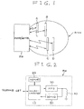
- a contactless IC card communication system includes a reader/writer RW provided on, for example, a telephone set.
- a given communication service area (a given communication coverage) provided by the reader/writer RW extends therefrom.
- four IC cards “A”, “B”, “C”, and “D” are placed in the communication service area.
- the IC cards “A”, “B”, “C” and “D” are prepaid cards for using a telephone set.
- the reader/writer RW can communicate with the IC cards “A”, “B", “C” and “D” by radio.
- a radio signal coming from the reader/writer RW is received by the antenna 60.
- the received radio signal is fed from the antenna 60 to the power supply circuit 70 and the demodulation circuit 80.
- the power supply circuit 70 generates DC power from the received radio signal, and stores the generated DC power.
- the power supply circuit 70 feeds the DC power to the demodulation circuit 80, the memory 90, the microcomputer 100, and the modulation circuit 110 to activate them.
- the microcomputer 100 includes a combination of an input/output port, a CPU, a ROM, and a RAM.
- the microcomputer 100 operates in accordance with a program stored in the ROM.
- the program has a first segment for implementing radio communications with the reader/writer RW.
- the program has a second segment designed to process requirements for the transmission of the information of the anti-collision technique used by the related IC card (the IC card "A”) and the identification information of the type of the related IC card (the IC card "A").
- the modulation circuit 110 receives output data (a baseband signal) from the microcomputer 100.
- the modulation circuit 110 subjects the output data from the microcomputer 100 to modulation, thereby converting the data (the baseband signal) into a radio signal.
- the modulation circuit 110 outputs the radio signal to the antenna 60.
- the radio signal is radiated by the antenna 60.
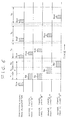
- an anti-collision technique used by the IC card “B” is the same as that used by the IC card “A”, and that anti-collision techniques used by the respective IC cards “C” and “D” are different from each other and are also different from that used by the IC cards “A” and “B”.
- the anti-collision technique used by the IC cards “A” and “B” is referred to as the first anti-collision technique.
- the anti-collision technique used by the IC card “C” is referred to as the second anti-collision technique.
- the anti-collision technique used by the IC card “D” is referred to as the third anti-collision technique.
- the microcomputer 100 reads out the data from the memory 90 in response to the anti-collision technique identification requirement signal Srw, and generates an answer signal Sa, Sb, Sc, or Sd (see Fig. 6) from the readout data.
- the microcomputer 100 outputs the answer signal Sa, Sb, Sc, or Sd (see Fig. 6) to the modulation circuit 110.
- the answer signal Sa, Sb, Sc, or Sd contains the information of the anti-collision technique used by the related IC card.
- the answer signal Sa outputted from the microcomputer 100 in the IC card “A” includes 8-bit serial-form data divided into 4-bit serial-form data Xa representing the anti-collision technique used by the IC card “A” (the first anti-collision technique), and 4-bit serial-form data Ya representing parameters of the IC card “A” (see Fig. 7).
- the former 4-bit portions of the 8-bit answer signals Sa and Sb are the same as shown in Fig. 7 since the first anti-collision technique is used in common by the IC cards "A" and "B".
- the time of the outputting of each of the answer signals Sa and Sb from the related microcomputer 100 is in a given time interval T1.
- the time interval T1 starts from the moment at which the recovered anti-collision technique identification requirement signal Srw is inputted into the microcomputer 100 from the demodulation circuit 80.
- the time of the outputting of the answer signal Sc from the related microcomputer 100 is in a given time interval T2 immediately following the time interval T1.
- the time of the outputting of the answer signal Sd from the related microcomputer 100 is in a given time interval T3 immediately following the time interval T2. This timing difference is provided by the differences among the first, second, and third anti-collision techniques.
- the modulation circuit 110 converts the anti-collision technique answer signal Sa into a corresponding radio answer signal Ra.
- the modulation circuit 110 feeds the radio answer signal Ra to the antenna 60.
- the antenna 60 radiates and transmits the radio answer signal Ra.
- the modulation circuit 110 converts the anti-collision technique answer signal Sc into a corresponding radio answer signal Rc.
- the modulation circuit 110 feeds the radio answer signal Rc to the antenna 60.
- the antenna 60 radiates and transmits the radio answer signal Rc.
- the card type identification requirement signal Sc ⁇ has a card type identification requirement code word corresponding to the first anti-collision technique (the anti-collision technique used by the IC cards "A” and "B").
- the time of the outputting of the card type identification requirement signal Sc ⁇ from the microcomputer 10 is in a given time interval T4.
- the time interval T4 starts from the moment at which the microcomputer 10 decides that an answer to the anti-collision technique identification requirement has come from the IC card using the first anti-collision technique (the IC card "A” or "B”).
- the microcomputer 10 determines the time at which the card type identification requirement signal Sc ⁇ should be outputted in accordance with the first anti-collision technique.
- the second command radio signal is received by the antenna 60.
- the received second command radio signal is fed from the antenna 60 to the demodulation circuit 80.
- the demodulation circuit 80 recovers the card type identification requirement signal Sc ⁇ from the received second command radio signal.
- the demodulation circuit 80 outputs the recovered card type identification requirement signal Sc ⁇ to the microcomputer 100.
- the microcomputer 100 reads out the data from the memory 90 in response to the card type identification requirement signal Sc ⁇ , and generates an answer signal Sca (see Fig. 6) from the readout data.
- the microcomputer 100 outputs the generated answer signal Sca to the modulation circuit 110.
- the answer signal Sca contains the identification information of the type of the IC card “A” which is related to the anti-collision technique (the first anti-collision technique) used by the IC card "A".
- the time of the outputting of the card type identification answer signal Sca is in the time interval T4 (see Fig. 6).
- the IC card “B” receives the second command radio signal from the reader/writer RW, and recovers the card type identification requirement signal Sc ⁇ from the received second command radio signal as the IC card "A” does.
- the microcomputer 100 reads out the data from the memory 90 in response to the card type identification requirement signal Sc ⁇ , and generates an answer signal Scb (see Fig. 6) from the readout data.
- the microcomputer 100 outputs the answer signal Scb to the modulation circuit 110.
- the answer signal Scb contains the information of the type of the IC card "B” which is related to the anti-collision technique (the first anti-collision technique) used by the IC card "B".
- the reader/writer RW sequentially implements the identification of the type of the IC card “C” and the identification of the type of the IC card “D”.
- the modulation circuit 30 converts the card type identification requirement signal Sc ⁇ into a corresponding command radio signal referred to as a third command radio signal.
- the modulation circuit 30 outputs the third command radio signal to the antenna 40.
- the third command radio signal is radiated by the antenna 40, being transmitted from the reader/writer RW.
- the third command radio signal is received by the antenna 60.
- the received third command radio signal is fed from the antenna 60 to the demodulation circuit 80.
- the demodulation circuit 80 recovers the card type identification requirement signal Sc ⁇ from the received third command radio signal.
- the demodulation circuit 80 outputs the recovered card type identification requirement signal Sc ⁇ to the microcomputer 100.
- the microcomputer 100 reads out the data from the memory 90 in response to the card type identification requirement signal Sc ⁇ , and generates an answer signal Scc (see Fig. 6) from the readout data.
- the microcomputer 100 outputs the generated answer signal Scc to the modulation circuit 110.
- the answer signal Scc contains the identification information of the type of the IC card “C” which is related to the anti-collision technique (the second anti-collision technique) used by the IC card “C”.
- the time of the outputting of the card type identification answer signal Scc is in the time interval T5 (see Fig. 6).
- the modulation circuit 110 converts the card type identification answer signal Scc into a corresponding radio answer signal Rac.
- the modulation circuit 110 feeds the radio answer signal Rac to the antenna 60.
- the antenna 60 radiates and transmits the radio answer signal Rac.
- the reader/writer RW implements the identification of the type of the IC card "D" as follows.
- the microcomputer 10 in the reader/writer RW accesses the data in the memory 20 which represents the relation of the third anti-collision technique with a requirement signal.
- the microcomputer 10 In response to the accessed data, the microcomputer 10 generates a signal Sc ⁇ of a requirement for the identification of the type of the IC card using the third anti-collision technique.
- the microcomputer 10 outputs the card type identification requirement signal Sc ⁇ to the modulation circuit 30 (see Fig. 6).
- the card type identification requirement signal Sc ⁇ has a card type identification code word corresponding to the IC card using the third anti-collision technique (the anti-collision technique used by the IC card "D"). As shown in Fig.
- the microcomputer 10 outputs the card type identification requirement signals Sc ⁇ , Sc ⁇ , and Sc ⁇ at respective different timings according to the differences among the first, second, and third anti-collision techniques.
- the antenna 40 in the reader/writer RW receives the radio answer signal Rad from the antenna 60 of the IC card "D".
- the received radio answer signal Rad is fed from the antenna 40 to the demodulation circuit 50.
- the demodulation circuit 50 recovers the card type identification answer signal Scd from the received radio answer signal Rad.
- the demodulation circuit 50 outputs the recovered card type identification answer signal Scd to the microcomputer 10.
- the microcomputer 10 generates a card type identification code word, which corresponds to the IC card "D", in response to the card type identification answer signal Scd.
- the microcomputer 10 writes data of the generated card type identification code word in the memory 20.
- the data of the generated card type identification word in the memory 20 will be used later in IC card control.
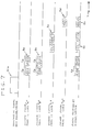
- a first step 200 of the program outputs an anti-collision technique identification requirement signal Srw to the modulation circuit 30. Alter the step 200, the program advances to a step 210.
- the step 210 decides whether or not an anti-collision technique answer signal in the first anti-collision technique is present. This decision relates to the anti-collision technique answer signals Sa and Sb transmitted from the IC cards "A" and "B".
- the program advances from the step 210 to a step 220. Otherwise, the program jumps from the step 210 to a step 230.
- the step 210 decides whether or not an anti-collision technique answer signal in the second anti-collision technique is present. This decision relates to the anti-collision technique answer signal Sd transmitted from the IC card "D".
- the program advances from the step 210 to the step 220. Otherwise, the program jumps from the step 210 to the step 230.
- the card type identification requirement signal Sc ⁇ has a card type identification requirement code word corresponding to the first anti-collision technique (the anti-collision technique used by the IC cards "A” and “B"). Then, the microcomputer 10 receives the card type identification answer signal Sca from the IC card "A”. The subroutine block 250 generates a card type identification code word, which corresponds to the IC card "A”, in response to the card type identification answer signal Sca. The subroutine block 250 writes data of the generated card type identification code word in the memory 20. The subroutine block 250 resets the flag related to the anti-collision technique answer signals Sa. Then, the microcomputer 10 receives the card type identification answer signal Scb from the IC card "B".
- the subroutine block 250 generates a card type identification code word, which corresponds to the IC card "B", in response to the card type identification answer signal Scb.
- the subroutine block 250 writes data of the generated card type identification code word in the memory 20.
- the subroutine block 250 resets the flag related to the anti-collision technique answer signals Sb. Then, the program advances from the subroutine block 250 to a step 260.
- the step 260 decides whether or not at least one IC card to be identified remains by referring to, for example, the flags related to the anti-collision technique answer signals Sa, Sb, Sc, and Sd.
- the program returns from the step 260 to the subroutine block 250. Otherwise, the program exits from the step 260, and then the current execution cycle of the program ends.
- the subroutine block 250 accesses the data in the memory 20, which represents the relation of the second anti-collision technique (the anti-collision technique used by the IC card "C") with a requirement signal, in response to the set flag related to the anti-collision technique answer signal Sc.
- the subroutine block 250 generates a signal Sc ⁇ of a requirement for the identification of the type of the related IC card (the IC card "C") in response to the accessed data.
- the subroutine block 250 outputs the card type identification requirement signal Sc ⁇ to the modulation circuit 30.
- the card type identification requirement signal Sc ⁇ has a card type identification requirement code word corresponding to the second anti-collision technique (the anti-collision technique used by the IC card "C").
- the microcomputer 10 receives the card type identification answer signal Scc from the IC card "C".
- the subroutine block 250 generates a card type identification code word, which corresponds to the IC card "C", in response to the card type identification answer signal Scc.
- the subroutine block 250 writes data of the generated card type identification code word in the memory 20.
- the subroutine block 250 resets the flag related to the anti-collision technique answer signals Sc. Then, the program advances from the subroutine block 250 to the step 260.
- the subroutine block 250 accesses the data in the memory 20, which represents the relation of the third anti-collision technique (the anti-collision technique used by the IC card "D") with a requirement signal, in response to the set flag related to the anti-collision technique answer signal Sd.
- the subroutine block 250 generates a signal Sc ⁇ of a requirement for the identification of the type of the related IC card (the IC card "D") in response to the accessed data.
- the subroutine block 250 outputs the card type identification requirement signal Sc ⁇ to the modulation circuit 30.
- the card type identification requirement signal Sc ⁇ has a card type identification requirement code word corresponding to the third anti-collision technique (the anti-collision technique used by the IC card "ID").
- Fig. 5 is a flowchart of the program in the microcomputer 100.
- a first step 300 of the program waits a given short time interval. Then, the program advances from the step 300 to a step 310.
- the step 320 reads out the data from the memory 90, and generates an answer signal Sa from the readout data.
- the step 320 determines a desired output timing on the basis of the readout data.
- the desired output timing depends on the anti-collision technique used by the present IC card (the IC card "A").
- the step 320 outputs the generated answer signal Sa to the modulation circuit 110 at a timing equal to the desired output timing.
- the answer signal Sa contains the information of the anti-collision technique used by the IC card "A" (that is, the first anti-collision technique).
- the step 340 decides whether or not a card type identification requirement signal Sc ⁇ is present. When a card type identification requirement signal Sc ⁇ is present, the program advances from the step 340 to a step 350. Otherwise, the program returns from the step 340 to the step 330.
- the step 350 reads out the data from the memory 90 in response to the card type identification requirement signal Sc ⁇ , and generates an answer signal Sca from the readout data.
- the step 350 determines a desired output timing on the basis of the readout data.
- the desired output timing depends on the identification information of the present IC card (the IC card "A").
- the step 350 outputs the generated answer signal Sca to the modulation circuit 110 at a timing equal to the desired output timing.
- the answer signal Sca contains the identification information of the type of the IC card "A" which is related to the anti-collision technique used by the related IC card "A" (that is, the first anti-collision technique).
- the telephone set on which the reader/writer RW is provided may be replaced by a dispenser or an automatic vending machine.
Landscapes
- Engineering & Computer Science (AREA)
- Physics & Mathematics (AREA)
- Toxicology (AREA)
- Health & Medical Sciences (AREA)
- Artificial Intelligence (AREA)
- Computer Vision & Pattern Recognition (AREA)
- General Physics & Mathematics (AREA)
- Theoretical Computer Science (AREA)
- Computer Networks & Wireless Communication (AREA)
- Electromagnetism (AREA)
- General Health & Medical Sciences (AREA)
- Computer Security & Cryptography (AREA)
- Radar Systems Or Details Thereof (AREA)
- Credit Cards Or The Like (AREA)
- Near-Field Transmission Systems (AREA)
Applications Claiming Priority (2)
| Application Number | Priority Date | Filing Date | Title |
|---|---|---|---|
| JP423398A JP3239294B2 (ja) | 1998-01-12 | 1998-01-12 | 非接触式icカード通信システム及びicカード通信方法 |
| JP423398 | 1998-01-12 |
Publications (3)
| Publication Number | Publication Date |
|---|---|
| EP0929048A2 true EP0929048A2 (de) | 1999-07-14 |
| EP0929048A3 EP0929048A3 (de) | 2000-03-01 |
| EP0929048B1 EP0929048B1 (de) | 2004-11-17 |
Family
ID=11578853
Family Applications (1)
| Application Number | Title | Priority Date | Filing Date |
|---|---|---|---|
| EP99100093A Expired - Lifetime EP0929048B1 (de) | 1998-01-12 | 1999-01-05 | System und Verfahren zur drahtlosen Kommunikation mit einer IC-Karte |
Country Status (4)
| Country | Link |
|---|---|
| US (1) | US6388562B1 (de) |
| EP (1) | EP0929048B1 (de) |
| JP (1) | JP3239294B2 (de) |
| DE (1) | DE69921866T2 (de) |
Cited By (3)
| Publication number | Priority date | Publication date | Assignee | Title |
|---|---|---|---|---|
| EP1111557A3 (de) * | 1999-12-10 | 2002-01-02 | Fujitsu Limited | Kontaklose IC-Karte und Verfahren zur deren Herstellung |
| EP1526474A1 (de) * | 2003-10-21 | 2005-04-27 | ATMEL Germany GmbH | Verfahren zur Auswahl eines oder mehrerer Transponder |
| WO2011084253A1 (en) | 2009-12-17 | 2011-07-14 | Alcatel-Lucent Usa Inc. | Crosstalk control method and apparatus using a bandwidth-adaptive precoder interface |
Families Citing this family (12)
| Publication number | Priority date | Publication date | Assignee | Title |
|---|---|---|---|---|
| JP2001136100A (ja) * | 1999-11-04 | 2001-05-18 | Matsushita Electronics Industry Corp | 情報通信処理方式 |
| MXPA02011493A (es) | 2001-11-28 | 2005-02-17 | Seiko Epson Corp | Comunicacion sin contacto entre el dispositivo y el cartucho que contiene componente consumible. |
| JP4692807B2 (ja) * | 2004-12-21 | 2011-06-01 | ソニー株式会社 | 接触式データ通信装置、送受信装置、および送受信方法 |
| KR101059872B1 (ko) * | 2005-01-03 | 2011-08-29 | 삼성전자주식회사 | 고유 식별자를 이용한 통신충돌방지 프로토콜 |
| JP4305854B2 (ja) * | 2005-01-19 | 2009-07-29 | 富士フイルム株式会社 | 画像管理装置及び方法 |
| US7274284B2 (en) * | 2005-02-04 | 2007-09-25 | Atmel Corporation | Method for RF card detection in a contactless system |
| JP5027398B2 (ja) | 2005-09-27 | 2012-09-19 | ルネサスエレクトロニクス株式会社 | Icタグ識別方法 |
| JP2007114821A (ja) * | 2005-10-18 | 2007-05-10 | Hitachi Ltd | Rfidタグ、rfidリーダ・ライタ、rfidシステムおよびrfidシステムの処理方法 |
| US20070297214A1 (en) * | 2006-06-09 | 2007-12-27 | Semiconductor Energy Laboratory Co., Ltd. | Semiconductor device |
| US9323964B2 (en) * | 2013-08-20 | 2016-04-26 | Cubic Corporation | Card detection and selection |
| CN107403119B (zh) * | 2017-06-13 | 2021-04-23 | 北京三快在线科技有限公司 | 一种智能卡信息读取方法及装置 |
| EP3493097B1 (de) * | 2017-11-29 | 2021-03-24 | ams AG | Verfahren zur drahtlosen bereitstellung von energie mittels funkfrequenzidentifikation (rfid) und rfid-system |
Family Cites Families (6)
| Publication number | Priority date | Publication date | Assignee | Title |
|---|---|---|---|---|
| US4638313A (en) * | 1984-11-08 | 1987-01-20 | Spacelabs, Inc. | Addressing for a multipoint communication system for patient monitoring |
| SG49786A1 (en) * | 1993-11-02 | 1998-06-15 | Nippondenso C Ltd | Communication system |
| JPH08123919A (ja) * | 1994-10-28 | 1996-05-17 | Mitsubishi Electric Corp | 非接触icカードシステムおよびその通信方法 |
| JPH08315090A (ja) * | 1995-05-23 | 1996-11-29 | Toshiba Corp | Icカードリーダライタおよびデータ伝送方法 |
| US5940006A (en) * | 1995-12-12 | 1999-08-17 | Lucent Technologies Inc. | Enhanced uplink modulated backscatter system |
| US5856788A (en) * | 1996-03-12 | 1999-01-05 | Single Chips Systems Corp. | Method and apparatus for radiofrequency identification tags |
-
1998
- 1998-01-12 JP JP423398A patent/JP3239294B2/ja not_active Expired - Lifetime
-
1999
- 1999-01-05 DE DE69921866T patent/DE69921866T2/de not_active Expired - Lifetime
- 1999-01-05 EP EP99100093A patent/EP0929048B1/de not_active Expired - Lifetime
- 1999-01-12 US US09/228,413 patent/US6388562B1/en not_active Expired - Fee Related
Cited By (3)
| Publication number | Priority date | Publication date | Assignee | Title |
|---|---|---|---|---|
| EP1111557A3 (de) * | 1999-12-10 | 2002-01-02 | Fujitsu Limited | Kontaklose IC-Karte und Verfahren zur deren Herstellung |
| EP1526474A1 (de) * | 2003-10-21 | 2005-04-27 | ATMEL Germany GmbH | Verfahren zur Auswahl eines oder mehrerer Transponder |
| WO2011084253A1 (en) | 2009-12-17 | 2011-07-14 | Alcatel-Lucent Usa Inc. | Crosstalk control method and apparatus using a bandwidth-adaptive precoder interface |
Also Published As
| Publication number | Publication date |
|---|---|
| DE69921866D1 (de) | 2004-12-23 |
| JP3239294B2 (ja) | 2001-12-17 |
| US6388562B1 (en) | 2002-05-14 |
| DE69921866T2 (de) | 2005-10-20 |
| EP0929048A3 (de) | 2000-03-01 |
| EP0929048B1 (de) | 2004-11-17 |
| JPH11203428A (ja) | 1999-07-30 |
Similar Documents
| Publication | Publication Date | Title |
|---|---|---|
| US6388562B1 (en) | Contactless IC card communication system and related method | |
| US6352202B2 (en) | Method and system for controlling contactless IC cards | |
| US8330581B2 (en) | IC tag, method of controlling the IC tag, and IC tag system | |
| EP4276678B1 (de) | Verfahren für etiketteninventar und zugehörige vorrichtung | |
| US6456191B1 (en) | Tag system with anti-collision features | |
| US7365642B2 (en) | Semiconductor integrated circuit, mobile module, and message communication method | |
| CN101517599B (zh) | 用于集成的读取器和标签的装置和方法 | |
| US20070274242A1 (en) | Multi-tag emulator | |
| US20080136599A1 (en) | Reader/writer apparatus, data access system, data access control method, and computer product | |
| US20120126952A1 (en) | Communication Method in RFID or Remote Sensor Systems | |
| US10085268B2 (en) | Communications device and communications system | |
| US7703690B2 (en) | Non-contact IC apparatus and control method | |
| WO2006110000A1 (en) | Contactless type integrated circuit card and method for communicating data by multiprotocol | |
| EP1675034A1 (de) | Kontaktdatenkommunikationsvorrichtung, Übertragungs- und Empfangsvorrichtung sowie Übertragungs- und Empfangsverfahren | |
| EP1780655A1 (de) | RFID-Tag, RFID-Schreib-/Lesegerät, RFID-System und Kommunikationsverfahren | |
| WO2001033725A1 (en) | Information communication system, noncontact ic card, and ic chip | |
| US10931331B2 (en) | Communication device and method | |
| JP4284745B2 (ja) | Icカード通信システム | |
| JP4116273B2 (ja) | 乱数発生装置を有する無線カード、この無線カード用の半導体装置、およびこの無線カードを用いた無線カードシステム | |
| JP4399065B2 (ja) | データキャリアの多数識別方法及びデータ通信システム | |
| JPH08167090A (ja) | 移動体識別方法 | |
| US7567792B2 (en) | Method for controlling the power supply of a mobile data memory, use of said method in an identification system having at least one mobile data memory | |
| JPH11167610A (ja) | Icカードシステム及びその通信方法 | |
| EP1502230B1 (de) | Verfahren zum inventarisieren einer mehrzahl von datenträgern | |
| JP2000148931A (ja) | カ―ド識別方法の改良 |
Legal Events
| Date | Code | Title | Description |
|---|---|---|---|
| PUAI | Public reference made under article 153(3) epc to a published international application that has entered the european phase |
Free format text: ORIGINAL CODE: 0009012 |
|
| AK | Designated contracting states |
Kind code of ref document: A2 Designated state(s): DE FR GB |
|
| AX | Request for extension of the european patent |
Free format text: AL;LT;LV;MK;RO;SI |
|
| PUAL | Search report despatched |
Free format text: ORIGINAL CODE: 0009013 |
|
| AK | Designated contracting states |
Kind code of ref document: A3 Designated state(s): AT BE CH CY DE DK ES FI FR GB GR IE IT LI LU MC NL PT SE |
|
| AX | Request for extension of the european patent |
Free format text: AL;LT;LV;MK;RO;SI |
|
| 17P | Request for examination filed |
Effective date: 20000828 |
|
| AKX | Designation fees paid |
Free format text: DE FR GB |
|
| RAP1 | Party data changed (applicant data changed or rights of an application transferred) |
Owner name: NEC TOKIN CORPORATION Owner name: HITACHI, LTD. Owner name: NIPPON TELEGRAPH AND TELEPHONE CORPORATION Owner name: DENSO CORPORATION |
|
| RAP1 | Party data changed (applicant data changed or rights of an application transferred) |
Owner name: NEC TOKIN CORPORATION Owner name: HITACHI, LTD. Owner name: NIPPON TELEGRAPH AND TELEPHONE CORPORATION Owner name: DENSO WAVE INCORPORATED |
|
| 17Q | First examination report despatched |
Effective date: 20030820 |
|
| GRAP | Despatch of communication of intention to grant a patent |
Free format text: ORIGINAL CODE: EPIDOSNIGR1 |
|
| GRAS | Grant fee paid |
Free format text: ORIGINAL CODE: EPIDOSNIGR3 |
|
| GRAA | (expected) grant |
Free format text: ORIGINAL CODE: 0009210 |
|
| AK | Designated contracting states |
Kind code of ref document: B1 Designated state(s): DE FR GB |
|
| REG | Reference to a national code |
Ref country code: GB Ref legal event code: FG4D |
|
| REF | Corresponds to: |
Ref document number: 69921866 Country of ref document: DE Date of ref document: 20041223 Kind code of ref document: P |
|
| ET | Fr: translation filed | ||
| PLBE | No opposition filed within time limit |
Free format text: ORIGINAL CODE: 0009261 |
|
| STAA | Information on the status of an ep patent application or granted ep patent |
Free format text: STATUS: NO OPPOSITION FILED WITHIN TIME LIMIT |
|
| 26N | No opposition filed |
Effective date: 20050818 |
|
| PGFP | Annual fee paid to national office [announced via postgrant information from national office to epo] |
Ref country code: GB Payment date: 20130102 Year of fee payment: 15 Ref country code: DE Payment date: 20130103 Year of fee payment: 15 Ref country code: FR Payment date: 20130204 Year of fee payment: 15 |
|
| REG | Reference to a national code |
Ref country code: DE Ref legal event code: R119 Ref document number: 69921866 Country of ref document: DE |
|
| GBPC | Gb: european patent ceased through non-payment of renewal fee |
Effective date: 20140105 |
|
| REG | Reference to a national code |
Ref country code: DE Ref legal event code: R119 Ref document number: 69921866 Country of ref document: DE Effective date: 20140801 |
|
| PG25 | Lapsed in a contracting state [announced via postgrant information from national office to epo] |
Ref country code: DE Free format text: LAPSE BECAUSE OF NON-PAYMENT OF DUE FEES Effective date: 20140801 |
|
| REG | Reference to a national code |
Ref country code: FR Ref legal event code: ST Effective date: 20140930 |
|
| PG25 | Lapsed in a contracting state [announced via postgrant information from national office to epo] |
Ref country code: FR Free format text: LAPSE BECAUSE OF NON-PAYMENT OF DUE FEES Effective date: 20140131 Ref country code: GB Free format text: LAPSE BECAUSE OF NON-PAYMENT OF DUE FEES Effective date: 20140105 |