EP0920131A2 - Circuit électrique comportant au moins une capacité commutée et son procédé de fonctionnement - Google Patents
Circuit électrique comportant au moins une capacité commutée et son procédé de fonctionnement Download PDFInfo
- Publication number
- EP0920131A2 EP0920131A2 EP98122682A EP98122682A EP0920131A2 EP 0920131 A2 EP0920131 A2 EP 0920131A2 EP 98122682 A EP98122682 A EP 98122682A EP 98122682 A EP98122682 A EP 98122682A EP 0920131 A2 EP0920131 A2 EP 0920131A2
- Authority
- EP
- European Patent Office
- Prior art keywords
- circuit
- switching pulse
- complementary
- switching
- signal
- Prior art date
- Legal status (The legal status is an assumption and is not a legal conclusion. Google has not performed a legal analysis and makes no representation as to the accuracy of the status listed.)
- Withdrawn
Links
- 239000003990 capacitor Substances 0.000 title claims abstract description 31
- 238000000034 method Methods 0.000 title claims abstract description 11
- 230000000295 complement effect Effects 0.000 claims abstract description 31
- 230000001105 regulatory effect Effects 0.000 claims abstract description 7
- 230000000903 blocking effect Effects 0.000 claims description 2
- 230000001934 delay Effects 0.000 claims description 2
- 230000003111 delayed effect Effects 0.000 description 6
- 238000010586 diagram Methods 0.000 description 6
- 230000005669 field effect Effects 0.000 description 5
- 230000003071 parasitic effect Effects 0.000 description 5
- 238000011144 upstream manufacturing Methods 0.000 description 4
- 230000008859 change Effects 0.000 description 2
- 230000007423 decrease Effects 0.000 description 2
- 230000004913 activation Effects 0.000 description 1
- 230000033228 biological regulation Effects 0.000 description 1
- 230000004048 modification Effects 0.000 description 1
- 238000012986 modification Methods 0.000 description 1
- 230000008569 process Effects 0.000 description 1
- 230000000630 rising effect Effects 0.000 description 1
Images


Classifications
-
- H—ELECTRICITY
- H03—ELECTRONIC CIRCUITRY
- H03H—IMPEDANCE NETWORKS, e.g. RESONANT CIRCUITS; RESONATORS
- H03H19/00—Networks using time-varying elements, e.g. N-path filters
- H03H19/004—Switched capacitor networks
Definitions
- the invention relates to an electrical circuit with at least one so-called switched capacitor.
- the invention also relates to a method for operating such an electrical circuit.
- it is an electrical circuit with at least one switched capacitor connected via a parallel circuit with two electronic, complementary switches is switched by complementary Switching pulses are controlled with a switching pulse generator, which receives a basic clock signal and from it a first switching pulse train as well as an almost complementary, second switching pulse train forms. It is also a method of operating one electrical circuit.
- SC switched capacitors
- the impedance of a capacitor is calculated the reciprocal of the product of frequency and capacity. Accordingly are integrated to simulate ohmic resistances Capacitors controlled by switches, so that a constant reloading process takes place at the capacitor. The frequency of the drive signal is matched to the capacitance of the capacitor so that the desired Impedance is reached.
- IGFET insulated gate field effect transistor
- CMOS field effect transistors two complementary ones connected in parallel Field effect transistors
- the present invention addresses problems in driving a switched capacitor with complementary transistor switches, which are controlled with complementary switching pulse trains.
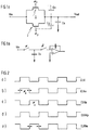
- Fig. 1a shows a switched capacitor C S with a first switching transistor 1, which is driven with a switching signal ⁇ n, to which a second switching transistor complementary to the first switching transistor is connected, which is driven with a complementary switching signal ⁇ p. Due to the complementary activation of the complementary transistors, both transistors are either closed at the same time or opened at the same time.
- FIG. 1b shows a schematic sketch of a circuit within an integrated circuit with a switched capacitance C S , which is preceded by a transistor switch and a transistor switch is connected downstream.
- An operational amplifier is located downstream of the switched capacitance.
- the circuit shown in Fig. 1a corresponds to the switching capacity C S with the upstream switch, which is driven by the switching pulse train ⁇ , where ⁇ in Fig. 1b contains the two signals ⁇ n and ⁇ p in Fig. 1a.
- the switch shown in FIG. 1b, which is driven by the signal ⁇ can be designed in a similar manner to the parallel connection of two complementary MOS field-effect transistors shown in FIG. 1a.
- Fig. 3 the signal curves for the switching pulses Wennn and ⁇ p are shown in the upper part, wherein it can be seen that in practice the signal edges do not run perpendicular to the time axis, but at an angle.
- the output voltage Vout of the circuit arrangement according to FIG. 1a is shown.
- This offset voltage is caused by different switching thresholds of the two switching transistors 1 and 2 (or in the case of a CMOS field effect transistor of the n-channel and the p-channel).
- the switching time corresponding to the threshold voltage V Tn is reached earlier than the switching time in the switching transistor 2 at which the switching signal ⁇ p reaches the threshold voltage V Tp relatively late.
- FIG. 4 shows the circuit according to FIG. 1b for the point in time in FIG. 3 is shown.
- the switching transistor 1 closes in the course of Trailing edge of the signal ⁇ n so that the resistance of this switch Roffn is very high (the resistance between drain and source of the Switching transistor 1).
- Ronp the resistance between the drain and source of the Switching transistor 2
- Roffn the turn-off resistor
- a capacitance C CFN (CF stands for "clock feed-through”) is located between the gate of the switching transistor 1 and the output node of the circuit. Between the gate of the lower switching transistor 2 and the output node of the circuit, there is a capacitance of C. CFP + C CTP (where CT stands for "charge transfer”).
- the present suggests Invention before to regulate the edges of the switching pulse trains so that a complete (if there is no permanent deviation) The offset voltage is compensated.
- the invention provides a method of operation a circuit with a switched capacitor, in which at least and preferably of at least one of the complementary switching pulse signals (e.g. ⁇ n) the leading edge and / or the trailing edge can be regulated in this way is that they depend on each other according to the output voltage parallel switches (1, 2) opposite the associated edge of the other of the complementary switching pulse signals ( ⁇ p) is shifted.
- the electronic switches are preferably complementary MOS-FETs.
- the delay circuit arranged in the output circuit for the first switching pulse train.
- the second switching pulse train then remains unchanged as it did Switching pulse generator is provided, and only the first switching pulse train is delayed relative to the second switching pulse train.
- a typical application example for switched capacitors are Filter circuits.
- Such a filter circuit with, for example, one Operational amplifier, in the feedback circuit of a capacitor and in its input circuit a simulated by a switched capacitor Resistance, is inventively in the form of a "replica" used as a control circuit.
- replica used as a control circuit.
- the edges of a switching pulse train are more or less delayed, with the aim that both switching transistors lock at the same time.
- the level change of the switching pulse ⁇ p takes place first at time t1.
- Vout increases compared to Vin, but only until the switching pulse ⁇ n begins to decrease.
- the two switching thresholds V Tn and V Tp are reached in quick succession at times t3 and t4.
- the n-channel or the switching transistor 1 in FIG. 1a is blocked, and there is no compensation for the p-channel or the switching transistor 2.
- the p-channel is also blocked, only the CF portion is compensated.
- the charge compensation for the p-channel then finally takes place between times t5 and t6 because the edge of the signal Signalsn is delayed compared to that of the signal ⁇ p.
- a basic clock signal CLK is applied to a NAND gate NAND1, at the same time, the inverted signal from CLK is applied to a NAND gate Given NAND2.
- the output signal from NAND 1 arrives via Delay element 3 and an inverter IN1 to a clock output for the signal CLKn.
- this is the clock signal or switching pulse signal regulated by a control signal "reg", which is generated by the circuit according to FIG. 7, which will be explained below becomes.
- the output signal from NAND1 also passes through two inverters IN7 and IN9 to a second input of NAND2.
- the second entrance from NAND1 also receives the output from NAND2 via two negators IN8 and IN10.
- Signal CLKNn The signal complementary or negated to the signal CLKn is called Signal CLKNn as a regulated switching pulse signal at the output of a Obtain negators IN2, upstream of which another delay element 4 which in turn is connected to the output of NAND2 is.
- a series connection of two inverters IN3 and IN5 turns one unregulated switching pulse signal CLKp from the output signal of NAND1 formed.
- the output signal from NAND2 becomes two Inverters IN6 and IN4 an unregulated clock signal or switching pulse signal CLKNp formed.
- FIG. 2 shows the input and output signals shown in FIG. 6, it can be seen in particular that the trailing edge of the signal CLKn is regulated with respect to CLKp and CLKNn with respect to CLKNp is.
- FIG. 7 shows the sketch of a circuit with which the control signal "reg" shown in FIG. 6 as the input signal for the delay elements 3 and 4 is obtained.
- the circuit shown in FIG. 7 is constructed in principle in the same way as the electrical circuit according to FIG. 1b, in which the switching capacitor Cs is to be connected in the input circuit of an operational amplifier of the filter circuit.
- the circuit shown in FIG. 7 contains the two switches in the input circuit or in the output circuit of the capacitor C S and the operational amplifier, a fixed reference voltage Vref being applied on the input side instead of the input voltage Vin in FIG. 1b.
- the output signals of the switching pulse generator according to FIG. 6 are in the given to the switching transistors shown in Fig. 7.
- 7 is a control signal at the output of the circuit of FIG obtained for the two delay circuits 3 and 4 in Fig. 6. If the signal “reg" rises, the switching pulse CLKn becomes corresponding greatly delayed, with the result that the amplitude of the control signal "reg” decreases and so the delay becomes smaller makes the delay element 3 in Fig. 6. The same applies to that negated signal CLKNn.
- edge control of the switching pulse train for the switching pulse signal CLKn or CLKNn is the origin of Avoid offset voltages on the switched capacitor.
Landscapes
- Engineering & Computer Science (AREA)
- Power Engineering (AREA)
- Pulse Circuits (AREA)
- Filters That Use Time-Delay Elements (AREA)
- Electronic Switches (AREA)
Applications Claiming Priority (2)
| Application Number | Priority Date | Filing Date | Title |
|---|---|---|---|
| DE19753279 | 1997-12-01 | ||
| DE19753279A DE19753279C2 (de) | 1997-12-01 | 1997-12-01 | Elektrische Schaltung mit mindestens einem geschalteten Kondensator und Verfahren zum Betreiben dieser Schaltung |
Publications (2)
| Publication Number | Publication Date |
|---|---|
| EP0920131A2 true EP0920131A2 (fr) | 1999-06-02 |
| EP0920131A3 EP0920131A3 (fr) | 2002-06-12 |
Family
ID=7850412
Family Applications (1)
| Application Number | Title | Priority Date | Filing Date |
|---|---|---|---|
| EP98122682A Withdrawn EP0920131A3 (fr) | 1997-12-01 | 1998-11-30 | Circuit électrique comportant au moins une capacité commutée et son procédé de fonctionnement |
Country Status (3)
| Country | Link |
|---|---|
| US (1) | US6191631B1 (fr) |
| EP (1) | EP0920131A3 (fr) |
| DE (1) | DE19753279C2 (fr) |
Families Citing this family (2)
| Publication number | Priority date | Publication date | Assignee | Title |
|---|---|---|---|---|
| JP4057212B2 (ja) | 2000-02-15 | 2008-03-05 | 三菱電機株式会社 | マイクロフォン装置 |
| US6515612B1 (en) | 2001-10-23 | 2003-02-04 | Agere Systems, Inc. | Method and system to reduce signal-dependent charge drawn from reference voltage in switched capacitor circuits |
Family Cites Families (5)
| Publication number | Priority date | Publication date | Assignee | Title |
|---|---|---|---|---|
| JPS5787620A (en) * | 1980-11-20 | 1982-06-01 | Fujitsu Ltd | Clock generating circuit |
| JPH0654961B2 (ja) * | 1985-04-10 | 1994-07-20 | 松下電器産業株式会社 | サンプルホ−ルド回路 |
| JPH0681018B2 (ja) * | 1986-03-31 | 1994-10-12 | 三菱電機株式会社 | 半導体集積回路 |
| JPH03204222A (ja) | 1989-12-29 | 1991-09-05 | Nec Corp | クロックドライバー回路 |
| JP3437719B2 (ja) * | 1996-07-24 | 2003-08-18 | 株式会社東芝 | アナログ・スイッチ回路 |
-
1997
- 1997-12-01 DE DE19753279A patent/DE19753279C2/de not_active Expired - Fee Related
-
1998
- 1998-11-30 EP EP98122682A patent/EP0920131A3/fr not_active Withdrawn
- 1998-12-01 US US09/203,552 patent/US6191631B1/en not_active Expired - Lifetime
Non-Patent Citations (2)
| Title |
|---|
| COLONNA V ET AL: "Clock feedthrough compensation with phase slope control in SC circuits" ELECTRONICS LETTERS, IEE STEVENAGE, GB, Bd. 32, Nr. 10, 9. Mai 1996 (1996-05-09), Seiten 864-865, XP006005137 ISSN: 0013-5194 * |
| HAYATO MASUNARI ET AL: "SWITCHED CAPACITOR CIRCUITS WITH COMPENSATOR FOR CLOCK FEEDTHROUGH EFFECTS" ELECTRONICS & COMMUNICATIONS IN JAPAN, PART II - ELECTRONICS, SCRIPTA TECHNICA. NEW YORK, US, Bd. 79, Nr. 1, 1996, Seiten 51-63, XP000590963 ISSN: 8756-663X * |
Also Published As
| Publication number | Publication date |
|---|---|
| US6191631B1 (en) | 2001-02-20 |
| EP0920131A3 (fr) | 2002-06-12 |
| DE19753279C2 (de) | 2001-03-08 |
| DE19753279A1 (de) | 1999-06-02 |
Similar Documents
| Publication | Publication Date | Title |
|---|---|---|
| DE3839888C2 (fr) | ||
| DE69122541T2 (de) | Statischer Schalter für mittlere Spannung | |
| DE2541131C2 (de) | Schaltungsanordnung zum Konstanthalten der Schaltverzögerung von FET-Inverterstufen in einer integrierten Schaltung | |
| DE2659207B2 (de) | In einem integrierten MOSFET-Schaltkreis ausgebildete Verzögerungsstufe | |
| DE4233850C1 (de) | Schaltungsanordnung zur Stromeinstellung eines monolithisch integrierten Padtreibers | |
| DE2553517B2 (de) | Verzögerungsschaltung mit Feldeffekttransistoren | |
| DE69216663T2 (de) | Schaltkreis | |
| DE69317075T2 (de) | Integrierte Pufferschaltung mit gesteuerten Anstiegs- und Abfallszeiten | |
| DE69216141T2 (de) | Variable Pegeltreiberschaltung für periodische Ansteuerung einer kapazitiven Last | |
| DE3017669C2 (de) | Verstärkerschaltungsanordnung | |
| DE10000020A1 (de) | Integrierte Gate-Treiberschaltung | |
| EP0854574A2 (fr) | Circuit d'attaque | |
| DE19753279C2 (de) | Elektrische Schaltung mit mindestens einem geschalteten Kondensator und Verfahren zum Betreiben dieser Schaltung | |
| EP0685782A2 (fr) | Regulateur de tension | |
| DE69513545T2 (de) | Verfahren und Schaltungsanordnung zur Verringerung transienter Ströme | |
| WO1999059249A1 (fr) | Procede et dispositif pour commuter un transistor a effet de champ | |
| DE10331544B3 (de) | Verfahren zum Ansteuern eines Transistors | |
| DE102004015318B3 (de) | Eingangsschaltung für eine elektronische Schaltung | |
| DE2033294A1 (de) | Auf Berührung ansprechende Steuerschal tung fur die Tonumhullende in elektronischen Musikinstrumenten | |
| EP0570402B1 (fr) | Procede et dispositif de conversion temps/tension | |
| DE3837080C2 (fr) | ||
| DE2936000C3 (de) | Schaltungsanordnung zur Ableitung eines Normiersignals | |
| DE19918025C2 (de) | Schaltungsanordnung mit einer Ansteuerung für einen Halbleiterschalter mit sourceseitiger Last | |
| DE69615345T2 (de) | Treiberschaltung für einen verschluss mit einem ferroelektrischen flüssigkristall | |
| DE2657281C3 (de) | MIS-Inverterschaltung |
Legal Events
| Date | Code | Title | Description |
|---|---|---|---|
| PUAI | Public reference made under article 153(3) epc to a published international application that has entered the european phase |
Free format text: ORIGINAL CODE: 0009012 |
|
| AK | Designated contracting states |
Kind code of ref document: A2 Designated state(s): AT BE CH CY DE DK ES FI FR GB GR IE IT LI LU MC NL PT SE |
|
| AX | Request for extension of the european patent |
Free format text: AL;LT;LV;MK;RO;SI |
|
| PUAL | Search report despatched |
Free format text: ORIGINAL CODE: 0009013 |
|
| AK | Designated contracting states |
Kind code of ref document: A3 Designated state(s): AT BE CH CY DE DK ES FI FR GB GR IE IT LI LU MC NL PT SE |
|
| AX | Request for extension of the european patent |
Free format text: AL;LT;LV;MK;RO;SI |
|
| RIC1 | Information provided on ipc code assigned before grant |
Free format text: 7H 03H 19/00 A, 7H 03K 17/16 B |
|
| 17P | Request for examination filed |
Effective date: 20021210 |
|
| AKX | Designation fees paid |
Designated state(s): FR GB IT |
|
| REG | Reference to a national code |
Ref country code: DE Ref legal event code: 8566 |
|
| 17Q | First examination report despatched |
Effective date: 20071218 |
|
| GRAP | Despatch of communication of intention to grant a patent |
Free format text: ORIGINAL CODE: EPIDOSNIGR1 |
|
| STAA | Information on the status of an ep patent application or granted ep patent |
Free format text: STATUS: THE APPLICATION IS DEEMED TO BE WITHDRAWN |
|
| 18D | Application deemed to be withdrawn |
Effective date: 20090601 |