EP0919804A1 - Inspection system for planar object - Google Patents
Inspection system for planar object Download PDFInfo
- Publication number
- EP0919804A1 EP0919804A1 EP98309393A EP98309393A EP0919804A1 EP 0919804 A1 EP0919804 A1 EP 0919804A1 EP 98309393 A EP98309393 A EP 98309393A EP 98309393 A EP98309393 A EP 98309393A EP 0919804 A1 EP0919804 A1 EP 0919804A1
- Authority
- EP
- European Patent Office
- Prior art keywords
- light source
- light
- camera
- optical axis
- reflector
- Prior art date
- Legal status (The legal status is an assumption and is not a legal conclusion. Google has not performed a legal analysis and makes no representation as to the accuracy of the status listed.)
- Withdrawn
Links
- 238000007689 inspection Methods 0.000 title abstract description 51
- 230000003287 optical effect Effects 0.000 claims abstract description 45
- 238000000034 method Methods 0.000 claims description 27
- 238000003384 imaging method Methods 0.000 claims description 12
- 238000012545 processing Methods 0.000 claims description 10
- 238000005286 illumination Methods 0.000 claims description 5
- 238000005259 measurement Methods 0.000 abstract description 7
- 230000007547 defect Effects 0.000 description 7
- 230000008569 process Effects 0.000 description 3
- 229910000679 solder Inorganic materials 0.000 description 3
- 230000032258 transport Effects 0.000 description 3
- 230000008901 benefit Effects 0.000 description 2
- 238000005266 casting Methods 0.000 description 2
- 238000010586 diagram Methods 0.000 description 2
- NJPPVKZQTLUDBO-UHFFFAOYSA-N novaluron Chemical compound C1=C(Cl)C(OC(F)(F)C(OC(F)(F)F)F)=CC=C1NC(=O)NC(=O)C1=C(F)C=CC=C1F NJPPVKZQTLUDBO-UHFFFAOYSA-N 0.000 description 2
- 238000007747 plating Methods 0.000 description 2
- 101100028477 Drosophila melanogaster Pak gene Proteins 0.000 description 1
- 238000007792 addition Methods 0.000 description 1
- 238000013459 approach Methods 0.000 description 1
- 230000008859 change Effects 0.000 description 1
- 230000002950 deficient Effects 0.000 description 1
- 238000006073 displacement reaction Methods 0.000 description 1
- 230000000694 effects Effects 0.000 description 1
- 230000007257 malfunction Effects 0.000 description 1
- 238000004519 manufacturing process Methods 0.000 description 1
- 239000000463 material Substances 0.000 description 1
- 238000012986 modification Methods 0.000 description 1
- 230000004048 modification Effects 0.000 description 1
- 230000002123 temporal effect Effects 0.000 description 1
Images


Classifications
-
- G—PHYSICS
- G01—MEASURING; TESTING
- G01N—INVESTIGATING OR ANALYSING MATERIALS BY DETERMINING THEIR CHEMICAL OR PHYSICAL PROPERTIES
- G01N21/00—Investigating or analysing materials by the use of optical means, i.e. using sub-millimetre waves, infrared, visible or ultraviolet light
- G01N21/84—Systems specially adapted for particular applications
- G01N21/88—Investigating the presence of flaws or contamination
Definitions
- This invention relates generally to an inspection system by optical means, for example for inspecting integrated circuits by imaging.
- IC packages such as Quad Flat Pack (QFP), Plastic Leadless Chip Carrier (PLCC), Small Outline IC (SOIC), Small Outline J-Lead (SOJ), DPAK, Small Outline Transistor (SOT), and their derivatives having leads protruding out from the IC package body.
- QFP Quad Flat Pack
- PLCC Plastic Leadless Chip Carrier
- SOIC Small Outline IC
- SOJ Small Outline J-Lead
- DPAK Small Outline Transistor
- SOT Small Outline Transistor
- An Integrated Circuit (IC) package typically has a square or rectangular plastic package moulded over the IC circuitry commonly known as the "die".
- the size of the package may range from 4x4mm square to 32x32mm square.
- Extending from the plastic package are leads that provide electrical connectivity from the die inside the IC package to the printed circuit boards (PCB). It is important for the IC package and the leads to possess accurate and consistent mechanical dimensions because of the use of highly automated PCB assembly machine to place and solder the ICs onto the PCB. Damaged, twisted, or out-of-place leads will likely lead to improper assembling and malfunction in the PCB assembly.
- the mechanical requirements are even more stringent.
- leads and categories of defects that have to be measured include coplanarity, lead pitch, terminal dimension, standoff, and others.
- Lead defects include bent leads, solder plating defects, swept leads, burr, and the like.
- IC lead inspection and measurement systems There are two major categories of IC lead inspection and measurement systems.
- One category uses laser-scanning approach.
- the other commonly used techniques include shadow casting and back illuminating the lead profiles onto imaging planes.
- some method uses lasers to scan the leads of an IC from the top.
- Another uses a back illuminated system with image doubler that increases the resolution of the image.
- Yet another method uses a lead inspection system to locate the leads with reference to a reference plate on which the device is mounted and a real-time reference which is used to provide a known correlation between the image pixels and linear measurement.
- One IC inspection system includes a displacement sensor in which the upward and downward coplanarity error of each lead is measured from a level change in the output signal of the sensor.
- Another system determines a position of at least one lead of an electronic component using shadow casting techniques.
- burrs on lead tips is another important factor that influences the electrical connectivity of an IC package to PCB. Therefore, there is a need for methods and systems for reliable inspection of ICs. especially for a method and methods and systems that can reliably inspect the bottom surface of the IC leads.
- the present invention seeks to provide an improved inspection system for inspecting, for example, integrated circuits.
- An embodiment of the apparatus for inspecting planar objects includes a camera for sensing an image of the planar object (e.g., IC), an oblique light source, and a reflector.
- the camera has an optical axis passing through the planar object normal to the plane of the object.
- the oblique light source radiates light on the planar object obliquely to the plane of the IC such that at least a portion of the oblique light source is positioned on one side of the optical axis.
- the reflector is positioned on the opposite side of the optical axis relative the portion of the oblique light source for reflecting light that crosses the optical axis from the oblique light source to the camera.
- the portion of the light source, the planar object, and the reflector are arranged such that at least a portion of the planar object interposes between the portion of the oblique light source and the reflector.
- the shape of that portion of the planar object is imaged on the camera by back-lighting. In this manner, the leads on the IC can be inspected.
- the apparatus includes an inspection datum having an upper and a lower surface and including a viewing window extending between said upper and lower surfaces; and a transport operable to move an object above the inspection datum across the viewing window.
- the object e.g., IC
- the object can be inspected by a viewer below the window as the object is in motion above and across the window. This is practicable because in this embodiment the object is not in contact with any object other than the pick up head of the transport that picks up the object, which in the case of an IC contacts only the top surface of the IC body.
- the image obtained by the viewer includes a plurality of image parts, with each image part being of a portion of the object.
- the image parts can be obtained from different optical paths obtained by the use of a plurality of reflectors each reflect an image part.
- the image parts can be all directed into the same viewer, e.g.. a charge coupled device (CCD).
- CCD charge coupled device
- the preferred inspection system is ideally suited to inspecting integrated circuits leads.
- the reflective means is adapted to obtain images of the respective sets of leads of the integrated circuit.
- the inspection system is suitable for all parts of leads such as gull-wing, j-bend and straight leads. Inspection can also be carried out on many types of packages such as thin QFP and very thin QFP or SOIC.
- An advantage of a preferred embodiment of the present invention is that the measurement of the leads can be carried out while the object (e.g., IC) is on the move and need not be stopped.
- the object e.g., IC
- a further advantage is that the object can be inspected without having to come into contact with any object such as a pedestal for inspection and therefore eliminates any possibility of lead damage due to contact with another object.
- the ability to inspect the integrated circuit package while it is moving reduces inspection time. Since the integrated circuit package does not need to come into contact with any object such as a pedestal during inspection, potential lead damages are totally eliminated.
- the bottom side of the IC and thus the bottom side of the leads can be viewed and inspected.
- the use of back-light to illumine the object (e.g., including IC leads) for inspection increases the stability and repeatability of the inspection results.
- True three-dimension (3D) lead geometry such as coplanarity, terminal dimension, pitch and other parameters can be measured.
- the inspection system provides a technique for inspecting the bottom portion of the side edges of the object and preferably without contacting the bottom parts of the object. Furthermore, an embodiment enables inspecting the inspection of the object while the object is in motion using a using a real time reference plane.
- the reference plane is built into the inspection system and is imaged together with the IC under inspection.
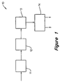
- Figure 1 illustrates in block diagram an embodiment of an apparatus for inspecting three-dimensional objects.
- the inspection system 10 includes four modules, namely the viewing optical module 11, the image acquisition module 12, the central processing module 13, and the control module 14.
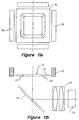
- the viewing optical module 11 includes an inspection datum 15 that has a sufficiently flat surface.
- the inspection datum 15 includes a frame 16 having an opening in its centre.
- the central opening in the inspection datum 15 is referred to as the viewing window 17.
- the viewing window 17 is an optically clear aperture allowing light of the desired wavelength to pass through.
- the size of the viewing window 17 is also adapted to be bigger than the size of the footprint of the IC 100 (not shown in Figure 2 but shown in Fig. 3 and Figure 4), which the system is arranged to inspect.
- the module 11 further includes reflectors 18, 19, 20 and 21 attached to the frame 16 just below the upper surfaces 22 of the datum 15. These reflectors 18, 19, 20, 21 are generally made up of either mirrors or prisms attached to the frame 16 adjacent the four sides of the viewing window 17.
- the optical module 11 of the embodiment shown in Figure 1 further includes a lens or len system 23 and video camera 24 and each of the reflectors 18, 19, 20, 21 reflects the image above the viewing window 17 into the lens 23 and further into the video camera 24.
- the lens 23 has telecentric property such that it is sufficiently tolerant to reasonable object distance variations.
- the video camera 24 is typically a Charged Coupled Device (CCD) camera which has a photo-sensitive array. The field of view of the video camera 24 encompasses the entire viewing window 17 and the four reflectors 18, 19, 20, 21.
- CCD Charged Coupled Device
- the optical module 11 further includes uniformly illuminating light source 25, which can have parts, which are positioned around the viewing window 17. These uniformly illuminating light source parts 25 are used for back-lighting the IC 100.
- Back-lighting is an illumination technique that light up an object silhouette for which dimensional measurement can be effectively carried out. In using back lighting technique, the object (i.e., the IC) to be measured is positioned between the viewer (camera) and the light source.
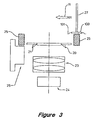
- the uniform light source 25 can be either mounted onto the inspection datum 15 or onto a movable platform 26 (as shown in Figure 3) surrounding the inspection datum.
- a movable platform 26 As shown in Figure 3, it is possible to lower the uniform light source 25 below the inspection datum 15 surface so that the inspection datum is clear of any object that may cause obstruction.
- the uniform light source 25 can be moved into place to illuminate the IC for imaging when the IC is proximate to the viewing window 17 (as in Figure 4).
- the uniform light source 25 can be moved out of the way to allow the IC to be move into or out of the viewing optical module before and after imaging.
- FIG. 3 and Figure 4 show embodiments illustrating how an IC can be transported for inspection.
- an IC 100 to be inspected is picked up from the top by means of a pickup head 27 such as a suction cup.
- a pickup head 27 such as a suction cup.
- suction heads and suction cups are known in the art and commonly used in the IC industry.
- the pickup head 27 transports the IC over the viewing window 17.
- the bottom side of the IC 100 remains clear for inspection without any obstruction.
- the IC 100 is aligned in parallel to the upper surface 22 of the inspection datum 15 with seating plane of the IC 100 largely parallel to this surface 22. A small spacing is maintained between the inspection datum 15 and the seating plane of the IC 100.
- the uniform light source 25 When the IC 100 is transported across the viewing window 17, no vertical movement is required to lower the IC 100 into the viewing window 17.
- the uniform light source 25 When the IC 100 is at the appropriate location above the viewing window 17, the uniform light source 25 is moved up by the platform 26 to its active position to provide back light for the video camera 24 to acquire the image of the IC 100. After the image is acquired. the uniform light source 25 is moved downward to its inactive position to provide a clear passage for the IC 100 to be transported out of the inspection datum 15.
- the light source 25 can be attached to the pickup head 27 and hence move together with the pickup head 27.
- the IC 100 when the IC is moved to the location of the viewing window 17, the IC 100 is located between the uniformly illuminating light source 25 and the reflector 18, 19, 20, 21.
- This is a back-lighting technique as the reflector obtains an image of the IC 100 and its leads 101 in silhouette (e.g., see Figure. 8).
- the video camera 24 hence images the silhouettes of the IC 100 and its leads 101 through the reflector 18, 19, 20, 21 and the lens 23.
- each of the reflectors 18, 19.20 21 views the leads 101 on the far side (i.e., the side edge remote from the corresponding reflector of the IC) hence forming a cross-looking geometry (see Figure 5).
- the reflector 20 reflects the silhouettes, created by light source from light source part 25A, of the IC leads 101A through the optical path 50 into the lens 23 and then into the video camera 24.
- the optical path 51 is a cross looking geometry where reflector 21 reflects light of light source part 25B passing by the leads 101B into the lens 23 and the video camera 24 as a silhouette.
- the IC consists of leads 101 on all its four sides, then all the four reflectors 18, 19, 20 and 21 will reflect their respective far side leads 101 into the lens 23 and the video camera 24.
- the viewing optical paths have a portion passing by the lead 101 inclining at a small oblique angle ⁇ with respect to the inspection datum 15.
- This oblique angle ⁇ further allows leads 101 above the IC 100 package bottom to be successfully imaged and measured. In practice, the oblique angle ⁇ is no more than 10 degrees.
- the inspection system 10 To enable the inspection system 10 to perform 3D inspection while the IC 100 is moving, the inspection system is adapted to cope with variations in positional shift when the image is acquired.
- the effect of the positional shift is illustrated in Figure 5.
- the variation in the lateral position is labelled L, which will cause a deviation of the optical path from 50 to 50a.
- the deviation D of the optical path if not compensated will cause an error in the Z measurement, which is related to the coplanarity of the IC 100.
- the system 10 includes compensation means.
- the compensation means is described below with reference to Figure 6, using reflectors 19 and 20 as an example. which are capable of imaging the orthogonal views of the leads 101.
- the optical path for viewing the comer lead 101 of the IC 100 is 52 for which the Y (the dimension into the page in Figure 5) and Z (the dimension on the plane of Figure 5 perpendicular to the Y axis and normal to the plane of the IC) co-ordinates can be measured.
- the corner lead 101 is located on the far side of the reflector 20.
- the reflector 20 views the corner lead 101 by optical path 53 for which the lateral position (regarding the X dimension) can be measured.
- the X, Y, Z co-ordinates of a lead can be determined.
- lead position 101 and lead position 102 are the positions of the same lead 101 in two adjacent images when the light source 25 and the reflector 20 are moved relative to the IC 100.
- the X, Y, Z positions of the lead 101 can be determined. Therefore, using this technique of cross-looking geometry, one is able to obtain three dimensional information on a part (e.g., leads of an IC) with only one light source and only one camera.
- Figure 6 shows a bottom view at the window 17 with an IC 100 at its centre for imaging.
- leads are shown on only one side on the side edges of the IC 100.
- the lead 101A is imaged by light passing along light path 53 onto the reflector 20 and imaged by light passing along light path 54 onto the reflector 19.
- the light paths 53 and 54 are substantially about 90 degrees to each other.
- the silhouette images reflected by the reflectors 18, 19, 20, 21 are not shown in this figure.
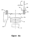
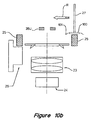
- the underside of the IC 100 can also be seen if a light is present to illuminate it, for example, as described later relating to Figure 10a.
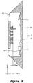
- the frame 16 may include reference points as illustrated in the Figure 7.
- the dynamic reference points 28, 29, 30, 31 are distributed on the four corners of the viewing window 17.
- the four dynamic reference points 28, 29, 30, 31 form a known precise reference plane.
- the distance between any two of these dynamic reference points are precisely known and are pre-stored in the central processing module 13.
- the dynamic reference points and the inspection datum 15 are preferably machined out from a single piece of rigid material so that high precision and flatness can be maintained.
- Figure 8 shows an image 60 acquired by the camera 24 i.e., as seen from a position under the IC
- Figure 9 is a part of this image showing specifically the image 61 reflecting from the reflector 20. through the lens 23 and onto the video camera 24.
- the dynamic reference point 28 is imaged onto point 62
- the dynamic point 29 is imaged onto point 63.
- the physical distance between the two dynamic reference points 28 and 29 is of a known value, A (see Figure 7).
- the distance (B) between imaged dynamic reference points 62 and 63 is measured in terms of pixels, which is a common term to denote the picture element in an digital array representing an image.
- the Y scale is equal to A/B. If A is measured in mm, then the unit for Y scale is mm per pixel. Similarly, the Y scale of this part of the image can be obtained by measuring the distance C, corresponding to how far the dynamic reference 63 extending out from the edge of the frame 16, in terms of pixel.
- the calibration procedure that has been described is equally applicable to all other three reflected sub images through reflectors 18, 19 and 21. Therefore, using the apparatus described one is able to obtain distances in absolute units (e.g., mm, micron) between points in the object in different co-ordinates.
- the image acquisition module 12 consists of a frame grabber (not shown in the figures) which receives the video signal from the video camera 24 and converts it into digital format which is known as a digital image corresponding to image 60 (see Figure 8). It is also common in the art that the video camera 24 may output digital format video signal.
- the frame grabber further transmits the digital image 60 for digital image processing and analysis to be carried out by the central processing module 13.
- a sensor may be used to sense the position of the IC 100 when it is moved across the inspection datum 15 (see arrow R in Figure 3) and triggers the image acquisition module 12 to acquire the image of the IC 100 when it is at an appropriate location above the viewing window 17.
- the trigger signal may also be derived from a motion controller of the pickup head 27 (see Figure 3).
- the motion controller of the pickup head 27 may have an encoder that monitors the position of the pickup head 27 and hence the location of the IC 100. It is also contemplated that the motion controller can be part of the central processing module 13 as well.
- the central processing module 13 processes the digital image 60 received from the image acquisition module 11.
- a task of the central processing module 13 is to compute the required parameters of the central processing module 13 will search and locate the positions of all leads 101 in the digital image 60. It will also detect the positions of all the dynamic reference points 27, 28, 29 and 30. Using two adjacent pair of reflected subimages, it further determines the lateral position regarding the X dimension of the IC 100.
- the compensation factors which involve X scale and Y scale are then computed. Using the compensation factors, the central processing module 13 computes the X, Y, Z co-ordinates of all the leads; apply the compensation factors and calculate the required parameters of the IC 100 such as coplanarity, pitch, terminal dimension and others.
- control module 14 One of the important functions of the control module 14 is to sense the position of the IC 100 so that it can trigger the image acquisition module 12 to acquire the image.
- the control module further provides signals to control the movement of the light source platform 26. If required when the IC 100 is moving into the inspection datum, the control module will activate the light source platform to move down so as to provide a clear passage for the pickup head 27 with the IC 100. Once the IC 100 has moved into the inspection datum, the control module 14 will signal the light source platform 26 to move up to illuminate the leads 101. Once the IC is directly above the viewing window 17, the control module will signal the image acquisition module 12 to capture the image. Once the image or images of the IC 100 have been captured, the control module 14 will signal the light source platform to lower itself which again will provide a clear passage for the IC 100 to be moved out of the inspection datum.
- a light can be included to illuminate the leads from a direction at a substantial angle to the light originating from the light source 25.
- the angle between light incident on or passing by closely a specific location by the two light sources is between 45 degree to 135 degree.
- An example would be to use a second light source to illuminate the leads from an angle about 90 degree to the light from the light source 25.
- Figure 10a shows an embodiment of such an apparatus.
- the light source 35U illuminates the IC 100 from the underside with front-lighting, so that the image when seen by the camera 24 can show the defects even on the surface of the leads or the underside surface of the IC.
- the light source 35U can have about a square shape similar to the light souse 25 to provide an even illumination on the leads and the underside of the IC 100.
- This technique of using two light source for example, with two light sources illuminating the IC leads so that light from the two sources illuminate the same lead at a substantial angle to one another, a defect on a lead or a portion of a lead that is bent and twisted in just the right way as to be difficult to detect using one light source can be easily detected using the other. Illumining the underside of the object with front-light, details (e.g., defects on the IC package) not previously observable can be seen. This provide an additional safeguard against allowing a defective product to pass without noticing the defect.
- a second light source provides a second image, which allows three dimensional information to be determined with only one picture of image received by the camera. In other words, in the same image received by the camera, observation is made from two different angles, thereby being able to see variations from standard in all three dimensions X, Y, and X even without moving the object between two imaging steps.
- a second light source 35V above the IC 100 in additional to light source 25 can be used to provide the illumination at an substantial angle relative to the light from light source 25.
- the IC 100 interposes between the second light source 35V and the camera 24 such that the light passes the leads 101 of the IC to the camera to form a silhouette type of image.
- the light source 35V have portions that can be moved out of the way to allow the IC 100 and the pickup head 27 to pass before and after imaging.
- the two light sources can be turned on at a different time so that they will not interfere with each other.
- This example illustrates the possibility of changing the physical layout of the described embodiments.
Landscapes
- Physics & Mathematics (AREA)
- Health & Medical Sciences (AREA)
- Life Sciences & Earth Sciences (AREA)
- Chemical & Material Sciences (AREA)
- Analytical Chemistry (AREA)
- Biochemistry (AREA)
- General Health & Medical Sciences (AREA)
- General Physics & Mathematics (AREA)
- Immunology (AREA)
- Pathology (AREA)
- Length Measuring Devices By Optical Means (AREA)
- Investigating Materials By The Use Of Optical Means Adapted For Particular Applications (AREA)
- Testing Or Measuring Of Semiconductors Or The Like (AREA)
Applications Claiming Priority (3)
| Application Number | Priority Date | Filing Date | Title |
|---|---|---|---|
| SG1997004179A SG67446A1 (en) | 1997-12-01 | 1997-12-01 | Cross optical axis inspection system for integrated circuits |
| SG9704179 | 1997-12-01 | ||
| US09/012,294 US6055055A (en) | 1997-12-01 | 1998-01-23 | Cross optical axis inspection system for integrated circuits |
Publications (1)
| Publication Number | Publication Date |
|---|---|
| EP0919804A1 true EP0919804A1 (en) | 1999-06-02 |
Family
ID=26665163
Family Applications (1)
| Application Number | Title | Priority Date | Filing Date |
|---|---|---|---|
| EP98309393A Withdrawn EP0919804A1 (en) | 1997-12-01 | 1998-11-17 | Inspection system for planar object |
Country Status (3)
| Country | Link |
|---|---|
| US (1) | US6055055A (enExample) |
| EP (1) | EP0919804A1 (enExample) |
| JP (1) | JPH11316112A (enExample) |
Cited By (1)
| Publication number | Priority date | Publication date | Assignee | Title |
|---|---|---|---|---|
| WO2004046643A1 (ja) * | 2002-11-21 | 2004-06-03 | Fuji Machine Mfg. Co., Ltd. | 電子回路部品像取得装置および方法 |
Families Citing this family (27)
| Publication number | Priority date | Publication date | Assignee | Title |
|---|---|---|---|---|
| US6915006B2 (en) * | 1998-01-16 | 2005-07-05 | Elwin M. Beaty | Method and apparatus for three dimensional inspection of electronic components |
| US6072898A (en) * | 1998-01-16 | 2000-06-06 | Beaty; Elwin M. | Method and apparatus for three dimensional inspection of electronic components |
| SG84530A1 (en) * | 1998-05-21 | 2001-11-20 | Agilent Technologies Inc | Cross optical axis inspection system for integrated circuits |
| US6538750B1 (en) * | 1998-05-22 | 2003-03-25 | Cyberoptics Corporation | Rotary sensor system with a single detector |
| US6243164B1 (en) * | 1998-07-13 | 2001-06-05 | Electro Scientific Industries | Method and system for determining lead coplanarity |
| WO2002039055A1 (en) * | 2000-10-25 | 2002-05-16 | Electro Scientific Industries, Inc. | Integrated alignment and calibration of optical system |
| US6532063B1 (en) | 2000-11-10 | 2003-03-11 | Semiconductor Technologies & Instruments | 3-D lead inspection |
| EP1220596A1 (en) * | 2000-12-29 | 2002-07-03 | Icos Vision Systems N.V. | A method and an apparatus for measuring positions of contact elements of an electronic component |
| US20020135757A1 (en) * | 2001-01-02 | 2002-09-26 | Robotic Vision Systems, Inc. | LCC device inspection module |
| US6573987B2 (en) * | 2001-01-02 | 2003-06-03 | Robotic Vision Systems, Inc. | LCC device inspection module |
| US7181083B2 (en) * | 2003-06-09 | 2007-02-20 | Eaton Corporation | System and method for configuring an imaging tool |
| US6856694B2 (en) * | 2001-07-10 | 2005-02-15 | Eaton Corporation | Decision enhancement system for a vehicle safety restraint application |
| WO2004049267A1 (de) * | 2002-11-23 | 2004-06-10 | Odas Gmbh | Verfahren zur fotografischen aufnahme eines zylinderförmigen, insbesondere plattenförmigen gegenstandes |
| US6944527B2 (en) * | 2003-11-07 | 2005-09-13 | Eaton Corporation | Decision enhancement system for a vehicle safety restraint application |
| US7532749B2 (en) * | 2003-11-18 | 2009-05-12 | Panasonic Corporation | Light processing apparatus |
| US7701564B2 (en) * | 2005-05-18 | 2010-04-20 | Hitachi Global Storage Technologies Netherlands B.V. | System and method for angular measurement |
| US8300921B2 (en) * | 2008-01-25 | 2012-10-30 | Panasonic Corporation | Inspection apparatus and inspection method |
| US8294760B2 (en) | 2009-04-21 | 2012-10-23 | Samsung Techwin Co., Ltd. | Electronic part recognition apparatus and chip mounter having the same |
| US8461532B2 (en) * | 2009-11-05 | 2013-06-11 | The Aerospace Corporation | Refraction assisted illumination for imaging |
| US8450688B2 (en) | 2009-11-05 | 2013-05-28 | The Aerospace Corporation | Refraction assisted illumination for imaging |
| US8138476B2 (en) * | 2009-11-05 | 2012-03-20 | The Aerospace Corporation | Refraction assisted illumination for imaging |
| JP5534919B2 (ja) * | 2010-04-22 | 2014-07-02 | 富士機械製造株式会社 | 電子部品の撮像判定方法及び部品実装機 |
| US9402036B2 (en) * | 2011-10-17 | 2016-07-26 | Rudolph Technologies, Inc. | Scanning operation with concurrent focus and inspection |
| US9007454B2 (en) | 2012-10-31 | 2015-04-14 | The Aerospace Corporation | Optimized illumination for imaging |
| JP6786593B2 (ja) | 2015-08-26 | 2020-11-18 | アーベーベー・シュバイツ・アーゲーABB Schweiz AG | 多視点による対象検査装置及び方法 |
| JP7199241B2 (ja) * | 2019-02-07 | 2023-01-05 | 株式会社東芝 | 半導体検査システム及び半導体検査装置 |
| WO2022187464A1 (en) * | 2021-03-03 | 2022-09-09 | Battelle Memorial Institute | Systems and methods for inspection of ic devices |
Citations (5)
| Publication number | Priority date | Publication date | Assignee | Title |
|---|---|---|---|---|
| US4686565A (en) * | 1984-05-22 | 1987-08-11 | Fujitsu Limited | Method and apparatus for visually examining an array of objects disposed in a narrow gap |
| US4696047A (en) * | 1985-02-28 | 1987-09-22 | Texas Instruments Incorporated | Apparatus for automatically inspecting electrical connecting pins |
| JPH0359446A (ja) * | 1989-07-28 | 1991-03-14 | Nec Corp | 集積回路パッケージピン検査装置 |
| US5185811A (en) * | 1990-12-27 | 1993-02-09 | International Business Machines Corporation | Automated visual inspection of electronic component leads prior to placement |
| US5563703A (en) * | 1994-06-20 | 1996-10-08 | Motorola, Inc. | Lead coplanarity inspection apparatus and method thereof |
Family Cites Families (3)
| Publication number | Priority date | Publication date | Assignee | Title |
|---|---|---|---|---|
| JPH03203399A (ja) * | 1989-12-29 | 1991-09-05 | Matsushita Electric Ind Co Ltd | 部品装着装置 |
| JPH03210410A (ja) * | 1990-01-12 | 1991-09-13 | Fujitsu Ltd | ピングリッドアレイ検査装置 |
| US5173796A (en) * | 1991-05-20 | 1992-12-22 | Palm Steven G | Three dimensional scanning system |
-
1998
- 1998-01-23 US US09/012,294 patent/US6055055A/en not_active Expired - Fee Related
- 1998-11-17 EP EP98309393A patent/EP0919804A1/en not_active Withdrawn
- 1998-11-27 JP JP10353940A patent/JPH11316112A/ja active Pending
Patent Citations (5)
| Publication number | Priority date | Publication date | Assignee | Title |
|---|---|---|---|---|
| US4686565A (en) * | 1984-05-22 | 1987-08-11 | Fujitsu Limited | Method and apparatus for visually examining an array of objects disposed in a narrow gap |
| US4696047A (en) * | 1985-02-28 | 1987-09-22 | Texas Instruments Incorporated | Apparatus for automatically inspecting electrical connecting pins |
| JPH0359446A (ja) * | 1989-07-28 | 1991-03-14 | Nec Corp | 集積回路パッケージピン検査装置 |
| US5185811A (en) * | 1990-12-27 | 1993-02-09 | International Business Machines Corporation | Automated visual inspection of electronic component leads prior to placement |
| US5563703A (en) * | 1994-06-20 | 1996-10-08 | Motorola, Inc. | Lead coplanarity inspection apparatus and method thereof |
Non-Patent Citations (1)
| Title |
|---|
| PATENT ABSTRACTS OF JAPAN vol. 015, no. 214 (P - 1209) 31 May 1991 (1991-05-31) * |
Cited By (1)
| Publication number | Priority date | Publication date | Assignee | Title |
|---|---|---|---|---|
| WO2004046643A1 (ja) * | 2002-11-21 | 2004-06-03 | Fuji Machine Mfg. Co., Ltd. | 電子回路部品像取得装置および方法 |
Also Published As
| Publication number | Publication date |
|---|---|
| US6055055A (en) | 2000-04-25 |
| JPH11316112A (ja) | 1999-11-16 |
Similar Documents
| Publication | Publication Date | Title |
|---|---|---|
| US6055055A (en) | Cross optical axis inspection system for integrated circuits | |
| US6141040A (en) | Measurement and inspection of leads on integrated circuit packages | |
| US5574801A (en) | Method of inspecting an array of solder ball connections of an integrated circuit module | |
| US7034272B1 (en) | Method and apparatus for evaluating integrated circuit packages having three dimensional features | |
| KR100334862B1 (ko) | 3각측량법에기초한3차원화상화를위한방법및시스템 | |
| US6671397B1 (en) | Measurement system having a camera with a lens and a separate sensor | |
| KR100283834B1 (ko) | 반도체칩의 본딩방법 및 그 장치 | |
| US7154596B2 (en) | Method and apparatus for backlighting and imaging multiple views of isolated features of an object | |
| JP2002529722A (ja) | 高さ感知センサを有するエレクトロニクス組立装置 | |
| US11982522B2 (en) | Three-dimensional measuring device | |
| EP0472041A2 (en) | Method and apparatus for detecting deformations of leads of semiconductor device | |
| JP7578718B2 (ja) | 実装基板検査装置および検査装置 | |
| TWI661176B (zh) | 三次元測定裝置、三次元測定方法及基板之製造方法 | |
| US6242756B1 (en) | Cross optical axis inspection system for integrated circuits | |
| US4875778A (en) | Lead inspection system for surface-mounted circuit packages | |
| US5402505A (en) | Semiconductor device lead inspection system | |
| WO2002029357A2 (en) | Method and apparatus for evaluating integrated circuit packages having three dimensional features | |
| JPH09511592A (ja) | 三次元物体の画像形成装置 | |
| US5838434A (en) | Semiconductor device lead calibration unit | |
| US20040099710A1 (en) | Optical ball height measurement of ball grid arrays | |
| EP1014438A2 (en) | A measurement system | |
| JP2002230523A (ja) | 検査装置 | |
| KR19990062659A (ko) | 집적 회로용 교차 광축 검사 시스템 | |
| JP3006566B2 (ja) | リード曲がり検査装置 | |
| KR102894745B1 (ko) | 스테레오 카메라를 사용하여 반도체 모듈을 검사하는 비전 시스템 |
Legal Events
| Date | Code | Title | Description |
|---|---|---|---|
| PUAI | Public reference made under article 153(3) epc to a published international application that has entered the european phase |
Free format text: ORIGINAL CODE: 0009012 |
|
| AK | Designated contracting states |
Kind code of ref document: A1 Designated state(s): BE CH DE LI NL |
|
| AX | Request for extension of the european patent |
Free format text: AL;LT;LV;MK;RO;SI |
|
| 17P | Request for examination filed |
Effective date: 19991129 |
|
| AKX | Designation fees paid |
Free format text: BE CH DE LI NL |
|
| RAP1 | Party data changed (applicant data changed or rights of an application transferred) |
Owner name: AGILENT TECHNOLOGIES, INC. |
|
| RAP1 | Party data changed (applicant data changed or rights of an application transferred) |
Owner name: AGILENT TECHNOLOGIES INC. |
|
| RAP1 | Party data changed (applicant data changed or rights of an application transferred) |
Owner name: AGILENT TECHNOLOGIES INC. A DELAWARE CORPORATION |
|
| RAP1 | Party data changed (applicant data changed or rights of an application transferred) |
Owner name: AGILENT TECHNOLOGIES, INC. (A DELAWARE CORPORATION |
|
| 17Q | First examination report despatched |
Effective date: 20040329 |
|
| STAA | Information on the status of an ep patent application or granted ep patent |
Free format text: STATUS: THE APPLICATION IS DEEMED TO BE WITHDRAWN |
|
| 18D | Application deemed to be withdrawn |
Effective date: 20040810 |