EP0917417B1 - Method for producing a mounting plate - Google Patents
Method for producing a mounting plate Download PDFInfo
- Publication number
- EP0917417B1 EP0917417B1 EP98120818A EP98120818A EP0917417B1 EP 0917417 B1 EP0917417 B1 EP 0917417B1 EP 98120818 A EP98120818 A EP 98120818A EP 98120818 A EP98120818 A EP 98120818A EP 0917417 B1 EP0917417 B1 EP 0917417B1
- Authority
- EP
- European Patent Office
- Prior art keywords
- mounting plate
- mounting
- producing
- circuit carrier
- depression
- Prior art date
- Legal status (The legal status is an assumption and is not a legal conclusion. Google has not performed a legal analysis and makes no representation as to the accuracy of the status listed.)
- Expired - Lifetime
Links
Images
Classifications
-
- H—ELECTRICITY
- H05—ELECTRIC TECHNIQUES NOT OTHERWISE PROVIDED FOR
- H05K—PRINTED CIRCUITS; CASINGS OR CONSTRUCTIONAL DETAILS OF ELECTRIC APPARATUS; MANUFACTURE OF ASSEMBLAGES OF ELECTRICAL COMPONENTS
- H05K7/00—Constructional details common to different types of electric apparatus
- H05K7/20—Modifications to facilitate cooling, ventilating, or heating
- H05K7/2039—Modifications to facilitate cooling, ventilating, or heating characterised by the heat transfer by conduction from the heat generating element to a dissipating body
- H05K7/20509—Multiple-component heat spreaders; Multi-component heat-conducting support plates; Multi-component non-closed heat-conducting structures
-
- H—ELECTRICITY
- H05—ELECTRIC TECHNIQUES NOT OTHERWISE PROVIDED FOR
- H05K—PRINTED CIRCUITS; CASINGS OR CONSTRUCTIONAL DETAILS OF ELECTRIC APPARATUS; MANUFACTURE OF ASSEMBLAGES OF ELECTRICAL COMPONENTS
- H05K7/00—Constructional details common to different types of electric apparatus
- H05K7/14—Mounting supporting structure in casing or on frame or rack
- H05K7/1417—Mounting supporting structure in casing or on frame or rack having securing means for mounting boards, plates or wiring boards
- H05K7/142—Spacers not being card guides
Definitions
- the thickness of a mounting plate determines the strength of a screw connection between the mounting plate and one in a mounting opening screw screwed into the mounting plate.
- the invention has for its object a method for generating specify a mounting plate of the type mentioned, through which the Strength of the screw connection between one or more screws and the mounting plate is increased.
- the essence of the invention is therefore the material thickness of the Increase mounting plate in the area of a mounting opening by at least one depression adjacent to this area, preferably a recess encircling this mounting opening into which Mounting plate is pressed.
- the mounting plate is advantageously cold deformed.
- the process is ideal for the production of mounting plates that as a heat sink for electronic components or for circuit carriers electronic components work.
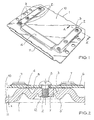
- the mounting plate 1 from FIG. 1 is made from a plate of uniform thickness, for example, made of an approximately 2 mm thick aluminum sheet.
- the Mounting plate 1 is first perforated, for example by drilling, to create the mounting holes 2.
- In a subsequent step become the upper surface side by cold working 10, d. H. the base of the mounting plate 1 outstanding and to this plane-parallel bearing surface 4 and the ring around the mounting openings 2 guided wells 3 formed.
- the recesses 3 are in the mounting plate by means of a stamp 1 pressed.
- FIG. 2 which is a sectional view of the mounting plate 1 along the section line A - A 'through one of the assembly openings 2, is formed by the formation of the recesses 3 material in the direction of respective mounting opening 2 shifted.
- This will make the material thickness y of the mounting plate 1 in the area of the mounting openings 2 by about 50% increased compared to the original thickness x of the mounting plate 1, in However, the area of the depressions 3 is reduced.
- the mounting plate 1 perpendicular to the base the mounting plate 1, moved so that under the recesses 3 on the lower surface side 11 of the mounting plate 1 annular material mountains 3 'arise that the lower surface 12 of the thickened areas overtop.
- the mounting plate 1 When handling the mounting plate 1 is through these mountains of material 3 'the risk of injury on the lower surface side 11 the mounting plate 1 resulting sharp edges of the wells 2 or the screws 5 screwed into the recesses 2 reduced.
- the mounting plate 1 forms a Lid for a housing, in which a populated with electronic components 7 Circuit carrier 6 is installed.
- the circuit carrier 6 is for this purpose with self-tapping screws 5, which go into the mounting holes 2 be screwed, connected to the mounting plate 1.
- the latter works at the same time as a heat sink, the thermal coupling between the Circuit carrier 6 and the mounting plate 1 is improved in that the circuit carrier 6 and the mounting plate 1 by means of a double-sided Adhesive tape 8, which before the assembly of the circuit carrier 6 applied to the degreased support surface 4 of the mounting plate 1 without bubbles will be glued together.
Description
Bei einer Montageplatte bestimmt deren Dicke die Festigkeit einer Schraubverbindung zwischen der Montageplatte und einer in eine Montageöffnung der Montageplatte eingeschraubten Schraube.The thickness of a mounting plate determines the strength of a screw connection between the mounting plate and one in a mounting opening screw screwed into the mounting plate.
Der Erfindung liegt die Aufgabe zugrunde, ein Verfahren zur Erzeugung einer Montageplatte der eingangs genannten Art anzugeben, durch das die Festigkeit der Schraubverbindung zwischen einer oder mehrerer Schrauben und der Montageplatte erhöht wird.The invention has for its object a method for generating specify a mounting plate of the type mentioned, through which the Strength of the screw connection between one or more screws and the mounting plate is increased.
Die Aufgabe wird durch die Merkmale im Patentanspruch 1 gelöst. Vorteilhafte Weiterbildungen und Ausgestaltungen ergeben sich aus den Unteransprüchen.The object is achieved by the features in claim 1. Advantageous further developments and refinements result from the Dependent claims.
Das wesen der Erfindung besteht demnach darin, die Materialdicke der Montageplatte im Bereich einer Montageöffnung zu erhöhen, indem mindestens eine an diesen Bereich angrenzende Vertiefung, vorzugsweise eine diese Montageöffnung ringförmig umschließende Vertiefung, in die Montageplatte eingepreßt wird. Hierzu wird die Montageplatte vorteilhafterweise kalt verformt.The essence of the invention is therefore the material thickness of the Increase mounting plate in the area of a mounting opening by at least one depression adjacent to this area, preferably a recess encircling this mounting opening into which Mounting plate is pressed. For this purpose, the mounting plate is advantageously cold deformed.
Das Verfahren eignet sich bestens zur Herstellung von Montageplatten, die als Kühlkörper für elektronische Bauteile oder für Schaltungsträger mit elektronischen Bauteilen wirken.The process is ideal for the production of mounting plates that as a heat sink for electronic components or for circuit carriers electronic components work.
Die Erfindung wird im folgenden anhand eines Ausführungsbeispiels unter Bezugnahme auf die Figuren näher beschrieben. Es zeigen:
- Figur 1
- eine erfindungsgemäße Montageplatte in perspektivischer Darstellung,
Figur 2- eine Detailansicht der Montageplatte aus Figur 1 mit einem Schaltungsträger in Schnittbilddarstellung.
- Figure 1
- a mounting plate according to the invention in a perspective view,
- Figure 2
- a detailed view of the mounting plate of Figure 1 with a circuit carrier in a sectional view.
Die Montageplatte 1 aus Figur 1 wird aus einer Platte einheitlicher Dicke,
beispielsweise aus einem ca. 2 mm dicken Aluminiumblech, gefertigt. Die
Montageplatte 1 wird dabei zunächst, beispielsweise durch Bohren, gelocht,
um die Montageöffnungen 2 zu erzeugen. In einem darauffolgenden Arbeitsschritt
werden durch Kaltverformung die die obere Oberflächenseite
10, d. h. die Grundfläche der Montageplatte 1 überragende und zu dieser
planparallele Auflagefläche 4 sowie die ringförmig um die Montageöffnungen
2 geführten Vertiefungen 3 gebildet.The mounting plate 1 from FIG. 1 is made from a plate of uniform thickness,
for example, made of an approximately 2 mm thick aluminum sheet. The
Mounting plate 1 is first perforated, for example by drilling,
to create the
Die Vertiefungen 3 werden dabei mittels eines Stempels in die Montageplatte
1 eingepreßt. Gemäß Figur 2, die ein Schnittbild der Montageplatte 1
entlang der Schnittlinie A - A' durch eine der Montageöffnungen 2, zeigt,
wird durch die Formung der Vertiefungen 3 Material in Richtung der
jeweiligen Montageöffnung 2 verschoben. Hierdurch wird die Materialdicke
y der Montageplatte 1 im Bereich der Montageöffnungen 2 um etwa 50%
gegenüber der ursprünglichen Dicke x der Montageplatte 1 erhöht, im
Bereich der Vertiefungen 3 jedoch verringert. Des weiteren wird Material
auch in Einpreßrichtung der Vertiefungen 3, d. h. senkrecht zur Grundfläche
der Montageplatte 1, verschoben, so daß unter den Vertiefungen 3 auf der
unteren Oberflächenseite 11 der Montageplatte 1 ringförmige Materialberge
3' entstehen, die die untere Oberfläche 12 der verdickten Bereiche
überragen. Beim Handhaben der Montageplatte 1 wird durch diese Materialberge
3' die Verletzungsgefahr an den auf der unteren Oberflächenseite 11
der Montageplatte 1 entstehenden scharfkantigen Rändern der Vertiefungen
2 oder den in die Vertiefungen 2 eingeschraubten Schrauben 5
verringert.The
Im vorliegenden Ausführungsbeispiel bildet die Montageplatte 1 einen
Deckel für ein Gehäuse, in welches ein mit elektronischen Bauteilen 7 bestückter
Schaltungsträger 6 eingebaut wird. Der Schaltungsträger 6 wird
hierzu mit selbstschneidenden Schrauben 5, die in die Montageöffnungen 2
eingeschraubt werden, mit der Montageplatte 1 verbunden. Letztere wirkt
gleichzeitig als Kühlkörper, wobei die thermische Kopplung zwischen dem
Schaltungsträger 6 und der Montageplatte 1 dadurch verbessert wird, daß
der Schaltungsträger 6 und die Montageplatte 1 mittels eines doppelseitigen
Klebebandes 8, welches vor der Montage des Schaltungsträgers 6
auf die entfettete Auflagefläche 4 der Montageplatte 1 blasenfrei aufgebracht
wird, miteinander verklebt werden.In the present exemplary embodiment, the mounting plate 1 forms a
Lid for a housing, in which a populated with
Claims (5)
- Method of producing a mounting plate (1), wherein in the region of at least one mounting opening (2) provided for screwing in a screw, the material thickness of the mounting plate (1) is increased by pressing in at least one depression (3) adjoining this region.
- Method according to Claim 1, characterised in that the at least one depression (3) is formed by cold pressing.
- Method according to Claim 1 or 2, characterised in that the at least one depression (3) is arranged in a ring shape around the at least one mounting opening (2).
- Method according to one of Claims 1 to 3, characterised in that at least in the region of the at least one mounting opening (2), a supporting surface (4) for a circuit carrier (6), which surface projects above a surface side (10) of the mounting plate (1) and is plane parallel to this, is formed by pressing.
- Method according to one of the preceding claims of producing a mounting plate (1) as cooling body for an electronic component (7) or for a circuit carrier (6) fitted with electronic components (7).
Applications Claiming Priority (2)
| Application Number | Priority Date | Filing Date | Title |
|---|---|---|---|
| DE19750433 | 1997-11-14 | ||
| DE19750433A DE19750433A1 (en) | 1997-11-14 | 1997-11-14 | Process for producing a mounting plate |
Publications (3)
| Publication Number | Publication Date |
|---|---|
| EP0917417A2 EP0917417A2 (en) | 1999-05-19 |
| EP0917417A3 EP0917417A3 (en) | 1999-12-15 |
| EP0917417B1 true EP0917417B1 (en) | 2004-09-08 |
Family
ID=7848700
Family Applications (1)
| Application Number | Title | Priority Date | Filing Date |
|---|---|---|---|
| EP98120818A Expired - Lifetime EP0917417B1 (en) | 1997-11-14 | 1998-11-03 | Method for producing a mounting plate |
Country Status (5)
| Country | Link |
|---|---|
| US (1) | US6158266A (en) |
| EP (1) | EP0917417B1 (en) |
| JP (1) | JPH11254049A (en) |
| DE (2) | DE19750433A1 (en) |
| ES (1) | ES2226056T3 (en) |
Families Citing this family (16)
| Publication number | Priority date | Publication date | Assignee | Title |
|---|---|---|---|---|
| FR2798814B1 (en) * | 1999-09-22 | 2001-11-16 | Valeo Vision | IMPROVEMENTS IN ELECTRONIC THERMAL DRAIN ASSEMBLIES, IN PARTICULAR FOR A MOTOR VEHICLE PROJECTOR DISCHARGE LAMP CONTROL MODULE |
| US6215663B1 (en) * | 2000-03-16 | 2001-04-10 | Philips Electronics North America Corporation | Printed circuit board assembly with improved thermal performance |
| DE10062699A1 (en) * | 2000-12-15 | 2002-07-04 | Conti Temic Microelectronic | Cooling device for electronic controllers has cooling plate deformation filling bearer opening in force-locking manner to form fixed mechanical connection between cooling plate and bearer |
| DE10109083B4 (en) * | 2001-02-24 | 2006-07-13 | Conti Temic Microelectronic Gmbh | Electronic module |
| US6588087B1 (en) * | 2001-10-02 | 2003-07-08 | Fisher Dynamics Corporation | Method of forming a side plate with integral boss |
| DE10206271A1 (en) * | 2002-02-15 | 2003-08-28 | Conti Temic Microelectronic | Thermal conductor connecting heat sink to substrate carrying electronic components used for engine valve control, has wavy profile and resilience |
| DE10300175B4 (en) * | 2003-01-08 | 2016-12-29 | Hella Kgaa Hueck & Co. | Electronic assembly with heat-dissipating housing part |
| JP4637926B2 (en) | 2008-03-28 | 2011-02-23 | 日立オートモティブシステムズ株式会社 | Electronic device and hydraulic unit |
| JP5612321B2 (en) * | 2010-01-27 | 2014-10-22 | 株式会社ヨロズ | Sleeve-integrated member and manufacturing method thereof |
| US20130128139A1 (en) * | 2011-11-18 | 2013-05-23 | Shenzhen China Star Optoelectronics Technology Co. Ltd. | Flat Panel Display Device, Stereoscopic Display Device, Plasma Display Device |
| US20130128147A1 (en) * | 2011-11-18 | 2013-05-23 | Shenzhen China Star Optoelectronics Technology Co., Ltd. | Flat Panel Display Device, Stereoscopic Display Device,and Plasma Display Device |
| US20130128182A1 (en) * | 2011-11-18 | 2013-05-23 | Shenzhen China Star Optoelectronics Technology Co., Ltd. | Back Frame of Flat Panel Display Device, Method for Manufacturing Back Frame, and Backlight System |
| US20130128420A1 (en) * | 2011-11-18 | 2013-05-23 | Shenzhen China Star Optoelectronics Technology Co. | Back Frame Of Flat Panel Display Device, Method For Manufacturing Back Frame, And Backlight System |
| US20130128138A1 (en) * | 2011-11-18 | 2013-05-23 | Shenzhen China Star Optoelectronics Technolog Co., LTD. | Flat Panel Display Device, Stereoscopic Display Device, Plasma Display Device |
| US9820419B2 (en) | 2014-10-30 | 2017-11-14 | Crystal Group, Inc. | Apparatus and method for utilizing commercial off the shelf circuit boards in a highly kinematic environment |
| DE102015218937A1 (en) | 2015-09-30 | 2017-03-30 | Continental Teves Ag & Co. Ohg | Electronic circuit carrier, heat sink and electrical device |
Family Cites Families (12)
| Publication number | Priority date | Publication date | Assignee | Title |
|---|---|---|---|---|
| US3611046A (en) * | 1966-09-16 | 1971-10-05 | Cross Electronics Inc | Apparatus for mounting and-or cooling electrical devices |
| DE2907415A1 (en) * | 1979-02-26 | 1980-09-04 | Wilhelm Schuetz | Hole stamped in metal sheet and provided with female thread - for making bolted connections which are impenetrable to gases or liquids |
| US4713960A (en) * | 1983-12-19 | 1987-12-22 | Gassaway J Scott | Method for forming a countersink in a plate |
| KR950014306B1 (en) * | 1985-12-17 | 1995-11-24 | 유티카 엔터프라이지즈, 인코오포레이티드 | Method and apparatus for body panel attachment |
| JPH02137620A (en) * | 1988-11-17 | 1990-05-25 | Tokin Corp | Metallic spacer and its working method |
| JPH03175698A (en) * | 1989-12-04 | 1991-07-30 | Mitsubishi Electric Corp | Printed wiring board |
| JPH05243756A (en) * | 1992-03-02 | 1993-09-21 | Nec Corp | Assembly for electronic parts |
| DE9406386U1 (en) * | 1994-04-16 | 1994-06-30 | Kloeckner Moeller Gmbh | Mounting plate for snapping a low-voltage switchgear mounted on it onto a top-hat rail |
| JPH0856086A (en) * | 1994-08-12 | 1996-02-27 | Fujitsu Ten Ltd | Mounting structure of wiring board to member |
| US5581877A (en) * | 1994-09-30 | 1996-12-10 | Allen-Bradley Company, Inc. | Method of fabrication of a circuit board adapted to receive a single in-line module |
| JP3288875B2 (en) * | 1994-11-28 | 2002-06-04 | 株式会社東芝 | Mounting structure of shield case |
| JPH09260871A (en) * | 1996-03-19 | 1997-10-03 | Kyocera Corp | Assembling structure of wiring board |
-
1997
- 1997-11-14 DE DE19750433A patent/DE19750433A1/en not_active Ceased
-
1998
- 1998-11-03 ES ES98120818T patent/ES2226056T3/en not_active Expired - Lifetime
- 1998-11-03 DE DE59811919T patent/DE59811919D1/en not_active Expired - Lifetime
- 1998-11-03 EP EP98120818A patent/EP0917417B1/en not_active Expired - Lifetime
- 1998-11-10 JP JP10355286A patent/JPH11254049A/en active Pending
- 1998-11-16 US US09/192,329 patent/US6158266A/en not_active Expired - Lifetime
Also Published As
| Publication number | Publication date |
|---|---|
| JPH11254049A (en) | 1999-09-21 |
| EP0917417A2 (en) | 1999-05-19 |
| DE19750433A1 (en) | 1999-06-02 |
| ES2226056T3 (en) | 2005-03-16 |
| EP0917417A3 (en) | 1999-12-15 |
| US6158266A (en) | 2000-12-12 |
| DE59811919D1 (en) | 2004-10-14 |
Similar Documents
| Publication | Publication Date | Title |
|---|---|---|
| EP0917417B1 (en) | Method for producing a mounting plate | |
| EP1061783B2 (en) | Ceramic-metal substrate, particularly multiple substrate | |
| EP0706214A2 (en) | Electronic module and chip card | |
| DE4220966C2 (en) | Method for producing a carrier plate for electrical components | |
| DE102012201172A1 (en) | Power semiconductor module with embossed base plate and method for producing a power semiconductor module with an embossed base plate | |
| EP0844808B1 (en) | Printed circuit board device | |
| DE3627372C3 (en) | Arrangement consisting of a printed circuit board, a heat sink and electronic components to be cooled | |
| DE3343034C2 (en) | Housing for semiconductor devices | |
| WO2020120417A1 (en) | Press platen for creating deep structures | |
| EP1887621A2 (en) | High performance electronics with cooling unit | |
| DE3445690C2 (en) | Process for the production of a carrier plate for a printed circuit | |
| EP0490984B1 (en) | Slotted punching plate | |
| DE19852832C2 (en) | Process for producing a metal-plastic laminate | |
| DE19615481C5 (en) | Arched metal-ceramic substrate | |
| DE102021109658B3 (en) | Method of manufacturing a semiconductor power device and semiconductor power device manufactured therewith and a tool part for a sintering press and use of a sintering press | |
| EP0792092A2 (en) | Process for manufacturing a composite arrangement | |
| DE19912957B4 (en) | Disc brake pad with a damping plate | |
| DE2752655A1 (en) | Electronic-component assembly for automated mass-production - has component in hole in support foil closed on one side by metal-plane heat sink | |
| DE3315414C2 (en) | ||
| DE29980179U1 (en) | Plate heat exchanger | |
| DE19511486A1 (en) | Mfr. of laminated circuit boards e.g. for control units in motor vehicle engineering | |
| DE3624756C2 (en) | ||
| EP0168722B1 (en) | Spacer element for glass-ceramic cooking unit or sink | |
| DE3609239A1 (en) | Process for producing a sheet-like matrix | |
| DE2819031A1 (en) | Die cutting clean and accurate openings in epoxy! resin plates - reinforced with glass fibres by following cutting die with oppositely directed oscillated clearing die |
Legal Events
| Date | Code | Title | Description |
|---|---|---|---|
| PUAI | Public reference made under article 153(3) epc to a published international application that has entered the european phase |
Free format text: ORIGINAL CODE: 0009012 |
|
| AK | Designated contracting states |
Kind code of ref document: A2 Designated state(s): DE ES FR GB IT SE |
|
| AX | Request for extension of the european patent |
Free format text: AL;LT;LV;MK;RO;SI |
|
| PUAL | Search report despatched |
Free format text: ORIGINAL CODE: 0009013 |
|
| AK | Designated contracting states |
Kind code of ref document: A3 Designated state(s): AT BE CH CY DE DK ES FI FR GB GR IE IT LI LU MC NL PT SE |
|
| AX | Request for extension of the european patent |
Free format text: AL;LT;LV;MK;RO;SI |
|
| 17P | Request for examination filed |
Effective date: 20000212 |
|
| RAP1 | Party data changed (applicant data changed or rights of an application transferred) |
Owner name: TEMIC TELEFUNKEN MICROELECTRONIC GMBH |
|
| AKX | Designation fees paid |
Free format text: DE ES FR GB IT SE |
|
| RAP1 | Party data changed (applicant data changed or rights of an application transferred) |
Owner name: CONTI TEMIC MICROELECTRONIC GMBH |
|
| GRAP | Despatch of communication of intention to grant a patent |
Free format text: ORIGINAL CODE: EPIDOSNIGR1 |
|
| GRAS | Grant fee paid |
Free format text: ORIGINAL CODE: EPIDOSNIGR3 |
|
| GRAA | (expected) grant |
Free format text: ORIGINAL CODE: 0009210 |
|
| REG | Reference to a national code |
Ref country code: SE Ref legal event code: TRGR |
|
| AK | Designated contracting states |
Kind code of ref document: B1 Designated state(s): DE ES FR GB IT SE |
|
| REG | Reference to a national code |
Ref country code: GB Ref legal event code: FG4D Free format text: NOT ENGLISH |
|
| GBT | Gb: translation of ep patent filed (gb section 77(6)(a)/1977) |
Effective date: 20040908 |
|
| REF | Corresponds to: |
Ref document number: 59811919 Country of ref document: DE Date of ref document: 20041014 Kind code of ref document: P |
|
| REG | Reference to a national code |
Ref country code: ES Ref legal event code: FG2A Ref document number: 2226056 Country of ref document: ES Kind code of ref document: T3 |
|
| PLBE | No opposition filed within time limit |
Free format text: ORIGINAL CODE: 0009261 |
|
| STAA | Information on the status of an ep patent application or granted ep patent |
Free format text: STATUS: NO OPPOSITION FILED WITHIN TIME LIMIT |
|
| ET | Fr: translation filed | ||
| 26N | No opposition filed |
Effective date: 20050609 |
|
| PGFP | Annual fee paid to national office [announced via postgrant information from national office to epo] |
Ref country code: ES Payment date: 20081121 Year of fee payment: 11 |
|
| PGFP | Annual fee paid to national office [announced via postgrant information from national office to epo] |
Ref country code: SE Payment date: 20081114 Year of fee payment: 11 Ref country code: IT Payment date: 20081122 Year of fee payment: 11 |
|
| PGFP | Annual fee paid to national office [announced via postgrant information from national office to epo] |
Ref country code: GB Payment date: 20081117 Year of fee payment: 11 |
|
| EUG | Se: european patent has lapsed | ||
| GBPC | Gb: european patent ceased through non-payment of renewal fee |
Effective date: 20091103 |
|
| PG25 | Lapsed in a contracting state [announced via postgrant information from national office to epo] |
Ref country code: GB Free format text: LAPSE BECAUSE OF NON-PAYMENT OF DUE FEES Effective date: 20091103 |
|
| REG | Reference to a national code |
Ref country code: ES Ref legal event code: FD2A Effective date: 20110304 |
|
| PG25 | Lapsed in a contracting state [announced via postgrant information from national office to epo] |
Ref country code: IT Free format text: LAPSE BECAUSE OF NON-PAYMENT OF DUE FEES Effective date: 20091103 |
|
| PG25 | Lapsed in a contracting state [announced via postgrant information from national office to epo] |
Ref country code: SE Free format text: LAPSE BECAUSE OF NON-PAYMENT OF DUE FEES Effective date: 20091104 |
|
| PG25 | Lapsed in a contracting state [announced via postgrant information from national office to epo] |
Ref country code: ES Free format text: LAPSE BECAUSE OF NON-PAYMENT OF DUE FEES Effective date: 20110303 |
|
| PG25 | Lapsed in a contracting state [announced via postgrant information from national office to epo] |
Ref country code: ES Free format text: LAPSE BECAUSE OF NON-PAYMENT OF DUE FEES Effective date: 20091104 |
|
| REG | Reference to a national code |
Ref country code: FR Ref legal event code: PLFP Year of fee payment: 18 |
|
| REG | Reference to a national code |
Ref country code: FR Ref legal event code: PLFP Year of fee payment: 19 |
|
| REG | Reference to a national code |
Ref country code: FR Ref legal event code: PLFP Year of fee payment: 20 |
|
| PGFP | Annual fee paid to national office [announced via postgrant information from national office to epo] |
Ref country code: DE Payment date: 20171130 Year of fee payment: 20 Ref country code: FR Payment date: 20171121 Year of fee payment: 20 |
|
| REG | Reference to a national code |
Ref country code: DE Ref legal event code: R071 Ref document number: 59811919 Country of ref document: DE |