EP0913946B1 - Frequenzsynthesizer für ein Mobilfunkendgerät - Google Patents
Frequenzsynthesizer für ein Mobilfunkendgerät Download PDFInfo
- Publication number
- EP0913946B1 EP0913946B1 EP98120249A EP98120249A EP0913946B1 EP 0913946 B1 EP0913946 B1 EP 0913946B1 EP 98120249 A EP98120249 A EP 98120249A EP 98120249 A EP98120249 A EP 98120249A EP 0913946 B1 EP0913946 B1 EP 0913946B1
- Authority
- EP
- European Patent Office
- Prior art keywords
- frequency
- memory
- pll
- phase locked
- frequency divider
- Prior art date
- Legal status (The legal status is an assumption and is not a legal conclusion. Google has not performed a legal analysis and makes no representation as to the accuracy of the status listed.)
- Expired - Lifetime
Links
- 230000009977 dual effect Effects 0.000 description 5
- 230000008859 change Effects 0.000 description 4
- 230000006870 function Effects 0.000 description 3
- 239000010453 quartz Substances 0.000 description 3
- VYPSYNLAJGMNEJ-UHFFFAOYSA-N silicon dioxide Inorganic materials O=[Si]=O VYPSYNLAJGMNEJ-UHFFFAOYSA-N 0.000 description 3
- 230000005540 biological transmission Effects 0.000 description 2
- 230000001419 dependent effect Effects 0.000 description 2
- 238000010586 diagram Methods 0.000 description 2
- 101000605345 Homo sapiens Prefoldin subunit 1 Proteins 0.000 description 1
- 101100274508 Oryza sativa subsp. japonica CKI1 gene Proteins 0.000 description 1
- 102100038255 Prefoldin subunit 1 Human genes 0.000 description 1
- 230000006978 adaptation Effects 0.000 description 1
- 230000008901 benefit Effects 0.000 description 1
- 230000015572 biosynthetic process Effects 0.000 description 1
- 230000008878 coupling Effects 0.000 description 1
- 238000010168 coupling process Methods 0.000 description 1
- 238000005859 coupling reaction Methods 0.000 description 1
- 238000011161 development Methods 0.000 description 1
- 230000018109 developmental process Effects 0.000 description 1
- 238000005516 engineering process Methods 0.000 description 1
- 230000004048 modification Effects 0.000 description 1
- 238000012986 modification Methods 0.000 description 1
- 230000004044 response Effects 0.000 description 1
- 238000003786 synthesis reaction Methods 0.000 description 1
- 230000009885 systemic effect Effects 0.000 description 1
Images

Classifications
-
- H—ELECTRICITY
- H03—ELECTRONIC CIRCUITRY
- H03L—AUTOMATIC CONTROL, STARTING, SYNCHRONISATION OR STABILISATION OF GENERATORS OF ELECTRONIC OSCILLATIONS OR PULSES
- H03L7/00—Automatic control of frequency or phase; Synchronisation
- H03L7/06—Automatic control of frequency or phase; Synchronisation using a reference signal applied to a frequency- or phase-locked loop
- H03L7/16—Indirect frequency synthesis, i.e. generating a desired one of a number of predetermined frequencies using a frequency- or phase-locked loop
- H03L7/22—Indirect frequency synthesis, i.e. generating a desired one of a number of predetermined frequencies using a frequency- or phase-locked loop using more than one loop
- H03L7/23—Indirect frequency synthesis, i.e. generating a desired one of a number of predetermined frequencies using a frequency- or phase-locked loop using more than one loop with pulse counters or frequency dividers
-
- H—ELECTRICITY
- H04—ELECTRIC COMMUNICATION TECHNIQUE
- H04B—TRANSMISSION
- H04B1/00—Details of transmission systems, not covered by a single one of groups H04B3/00 - H04B13/00; Details of transmission systems not characterised by the medium used for transmission
- H04B1/38—Transceivers, i.e. devices in which transmitter and receiver form a structural unit and in which at least one part is used for functions of transmitting and receiving
- H04B1/40—Circuits
- H04B1/403—Circuits using the same oscillator for generating both the transmitter frequency and the receiver local oscillator frequency
Definitions
- the invention relates to a frequency synthesizer with a Double PLL arrangement, each in the feedback branch a first counter or a second counter for optional frequency adjustment having.
- Such a double PLL arrangement ( P hee L ocked L oop) is used for example in mobile radio technology for frequency synthesis in mobile devices.
- the basic arrangement of the essential elements of a double PLL is described for example in the article by Wilfried Blaesner, frequency synthesizer for mobile radio, electronics, 10/1998, pages 108 to 112, in particular Figure 2.
- one PLL arrangement serves as a high-frequency PLL, which is referred to below as RF-PLL, and the other as an intermediate-frequency PLL, which is referred to below as IF-PLL.
- the double PLL arrangement the different frequencies for transmitting and receiving and additionally the channel-dependent frequencies are set.
- a first mixing stage cooperating with a first local oscillator and a mixing stage cooperating with a second local oscillator are present in the receiving section.
- the mobile terminals which are also commonly called radio terminals (RT), to the specific frequency ranges, adapted the mobile radio systems, referred to as a band become. That is, the frequency synthesizer of a mobile station one mobile radio system generates another Frequencies as the frequency synthesizer of another mobile station.
- known mobile radio systems differ even in other operating parameters, such as the reference frequency, Channel frequency and the like. A mobile station So it can only be within a specific mobile system be used.
- GSM Global System for Mobile Communications
- DCS 1800 D igital C ellular S ystem 1800
- a frequency synthesizer which several cascaded oscillator stages, each with a so-called contains phase-locked loop.
- the of the oscillator stages generated frequencies can be controlled by frequency dividers to be changed.
- These from the cascaded oscillator stages generated frequencies are a common output oscillator supplied, which provides an output frequency, the a load, e.g. B. an oscilloscope, is supplied.
- the oscillator stages especially when adjusting the frequency to be output, it comes to short periods the instability, resulting in several cascaded oscillator stages can cause significant disturbances. This should be prevented to a stable output frequency too to deliver on a change in the frequency to be output.
- the invention is based on the object, a mobile radio terminal of the type mentioned and a frequency synthesizer for use in such a mobile radio terminal, which in mobile radio systems with different network frequencies and / or other operating parameters as possible easy handling can be used.
- the invention has the advantage that, depending on control data, which are sent by a base station without the help of User automatically switch to the frequency range or the relevant operating parameters of the mobile system concerned he follows.
- the user can therefore use the mobile station as a dual-band or dual-mode mobile terminal in in the same way both in the area of a mobile radio system as well as the other mobile radio system without him must try to adapt or switch.
- a basic idea of the invention is therefore that of the base station for basic initialization the necessary Divisor values for the frequency divider of the dual PLL to the mobile station be transmitted and stored there. in the later operation of the base station is basically only still transmits a single control value in the mobile station, via which the selection of the stored divider values and in addition, if necessary, the change and switching be caused further operating parameters.
- a change the divider values for the high frequency part of the double PLL (RF-PLL) caused by a corresponding link with the frequency dividers of the intermediate frequency part of the double PLL (IF-PLL) automatically changes the associated divider values in the IF-PLL.
- the storage of the divider values takes place in the simplest case in individual registers, which have a multiplexer under Control by the base station to be selected. in principle but is any other type of memory and memory drive suitable to the required divisor values and make logical links.
- a preferred embodiment of the invention for use the mobile terminal in the dual band for the GSM mobile radio system and the DCS 1800 Mobile Radio System is that three registers for recording different counter values in the PLL counter of the intermediate frequency part are installed. It In this way three basic frequencies can be generated sufficient to the mobile station in both mobile standards to operate.
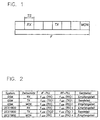
- a time frame F for the GSM and DCS 1800 standard from eight time slots TS there is a time frame F for the GSM and DCS 1800 standard from eight time slots TS.
- the second time slot RX for the receive mode the mobile station for signals from the base station intended.
- the fifth time slot TX is the transmission mode reserved and the eighth time slot MON is for monitor operation used.
- the ones used in send and receive mode Frequencies are different within a mobile radio system.
- the frequencies are in the transmission mode different according to the GSM standard and according to the DCS 1800 standard.
- the table according to FIG. 2 in conjunction with FIG. 3 shows, are therefore in the PLL arrangement in the present example of the intermediate frequency part IF-PLL three different frequencies to generate that for the device architecture once be determined.
- the table further illustrates that at Applications for other mobile systems, not on here in principle, six different frequencies for the PLL arrangement of the high-frequency part RF-PLL and six additional frequencies for the PLL arrangement of the intermediate frequency range IF-PLL may be required.
- the first column in FIG. 2 indicates which mobile radio system and with that which band is concerned.
- the second column contains the associated time slots RX, TX and MON.
- the third and fourth column are the individual Time slots assigned, systemic frequencies of the IF-PLL or the RF-PLL specified.
- the last column refers to the associated circuit part of the mobile radio terminal, in which the frequencies contained in the associated line be used.
- the frequency f LO1 of the RF PLL depends on the time slots and the mobile radio systems and is different in each case.
- the frequency f LO1 (RX) in the timeslots RX and MON of the GSM standard and in the timeslots RX and MON of the DCS 1800 standard is the same.
- TX of the GSM standard a different frequency f LO2 (TX) 1 in the GSM standard and a third frequency f LO2 (TX) 2 in the TX time slot of the DCS 1800 standard are used.
- the frequency synthesizer of the mobile station must therefore generate three fixed intermediate frequencies, which are set once for the device architecture in the basic initialization.
- the clock of a quartz Q is supplied via a counter R1 to a PLL arrangement of the high-frequency part (RF-PLL).
- RF-PLL high-frequency part
- RF-CNT high-frequency part
- Its output signal PD1 is fed via a filter LF1 a local, spanungswinen oscillator LO1, from the output of the frequency f LO1 is fed back to the counter RF-CNT.
- the output of the quartz is applied to a further divider R2 of the intermediate frequency part IF-PLL.
- the quartz clock of, for example, 130 MHz is divided into a typical channel frequency f ch of 200 kHz for the relevant mobile radio network.
- the contents of divider R1, R2 remain unchanged throughout the operation.
- the intermediate frequency part IF-PLL is another adjustable counter IF-CNT, which is connected together with the divider R2 to another phase detector TFD2. Its output signal PD2 is connected to a further filter LF2 and another local, voltage-controlled oscillator LO2, the frequency f LO2 is fed back to the other counter IF-CNT.
- the memory device in the present example in the RF-PLL from an input side shift register RF-SR, which is a data register downstream RF-DR, which is used for data transfer to the counter RF-CNT.
- the memory device consists of an input-side shift register IF-SR, which is followed by three data registers IF-DR1, IF-DR2, IF-DR3 which can be controlled via an address decoder ADR-DEC.
- IF-DR1, IF-DR2, IF-DR3 which can be controlled via an address decoder ADR-DEC.
- ADR-DEC address decoder
- one of these data registers is selected via a multiplexer MUX to transfer its contents to the counter IF-CNT.
- the multiplexer MUX can be controlled alternatively or in combination in two ways via a decoder DEC.
- predetermined register locations B n of the data register RF-DR which correspond to predetermined bit positions of the register contents, are connected to the decoder DEC via lines LTG1.
- these are two high-order bit positions of the content of the data register RF-DR.
- the most significant register location is provided in this example for selecting an output interface PORTS, which, together with a line LTG2 leading to the decoder DEC, serves to select externally available control signals OSW, BSW.
- the control of the decoder DEC takes place via control bits, in addition to the divisor value in the data register RF-DR be enrolled. Therefore, the relevant registers RF-SR and RF-DR correspondingly more registers as the number of bits of divisor values.
- the required divider values for the IF-PLL are successively written into the shift register IF-SR via the serial control unit SCL.
- column 3 there are three divisor values which are stored by the shift register IF-SR in the three data registers IF-DR in conjunction with the address decoder ADR-DEC.
- Each of the shift registers IF-DR thus contains a divider value for generating the frequencies f LO2 (RX), f LO2 (TX) 1 and f LO2 (TX) 2.
- the new frequency f LO1 is generated for each time slot RX, TX and MON, as shown in column 4 of FIG.
- the divider values to be written into the counter RF-CNT for this purpose come from the serial control unit SCL in the manner described above. If the respective divider value from the shift register RF-SR is written in the data register RF-DR, necessary for controlling the decoder DEC registries are activated and it is done automatically through the associated data register IF-DR via the multiplexer MUX to the counter IF-CNT so that the divisor value required for the IF PLL is written into the counter IF-CNT. This results in the desired change of the frequency f LO2 of the IF PLL.
- the external signal TRX can be used for decoder control.
- the signals selected via the output circuit PORTS OSW, BSW can serve to further components of the concerned Device to the parameters of the respective mobile radio system switch, such as filters, oscillators and like. This switchover then takes place automatically in Dependence on the contents of the corresponding registries of the data register RF-DR in the RF-PLL.
- a divider value is written via the serial control unit SCL, the shift register RF-SR and the data register RF-DR, which generates the frequency f LO1 (RX) 1 causes.
- the multiplexer MUX is controlled by the corresponding bits in the data register RF-DR via the decoder DEC in such a way that the divider value required to generate the frequency f LO1 (RX) is written into the counter IF-CNT by the corresponding data register IF-DR , If, for example, the DCS 1800 standard and the time slot TX are switched, then the required divider values are written into the counters RF-CNT and IF-CNT in the same way to produce the frequencies f LO1 (TX) 2 and f LO2 (TX ) 2.
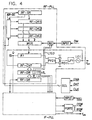
- the switching of the divider R1 of the RF-PLL is analogous to that described in connection with FIG. 3 switching the IF-PLL. Accordingly, a memory is provided which is assigned the required divider values during a basic initialization. In operation, one of the divider values is selected in each case and written to the divider R1. The selection is again effected automatically using predetermined register locations B ' n and / or via an external selection signal DM.
- the memory device consists of an input-side shift register RF-SR 'and three downstream data registers RF-DR, which are selected via an address decoder ADR-DEC in the basic initialization.
- ADR-DEC address decoder
- one of these three data registers IF-DR is then connected via a multiplexer MUX to the divider R1 for writing the corresponding divider value.
- the multiplexer MUX in turn is controlled via a decoder DEC, which is the input side to the corresponding register B ' n of the data register RF-DR and / or an input circuit INPUT acted upon.
- DEC decoder
Landscapes
- Stabilization Of Oscillater, Synchronisation, Frequency Synthesizers (AREA)
- Channel Selection Circuits, Automatic Tuning Circuits (AREA)
Description
- Fig. 1
- zeigt schematisch einen Zeitrahmen des GSM- und DCS 1800-Standards;
- Fig. 2
- zeigt anhand einer Tabelle die in einem Dual-Band zu generierenden Frequenzen;
- Fig. 3
- zeigt schematisch anhand eines Blockschaltbildes einen Frequenzsynthesizer für ein Dual-Band-Mobilfunkendgerät; und
- Fig. 4
- zeigt schematisch anhand eines Blockschaltbildes einen Frequenzsynthesizer für ein Dual-Mode-Mobilfunkendgerät.
Dessen Ausgangssignal PD1 wird über einen Filter LF1 einem lokalen, spanungsgesteuerten Oszillator LO1 zugeführt, von dessen Ausgang die Frequenz fLO1 auf den Zähler RF-CNT zurückgeführt ist. In gleicher Weise liegt der Ausgang des Quarzes an einem weiteren Teiler R2 des Zwischenfrequenzteils IF-PLL an. In beiden Teilern R1, R2 wird der Quarztakt von beispielsweise 130 MHz auf eine für das betreffende Mobilfunknetz typische Kanalfrequenz fch von 200 kHz geteilt. Die Inhalte der Teiler R1, R2 bleiben während des gesamten Betriebs unverändert.
selbstätig eingeschrieben wird.
Claims (7)
- Frequenzsynthesizer für ein Mobilfunkendgerät mit einer ersten Phasenregelschleife (RF-PLL) zur Erzeugung eines Hochfrequenzsignals (fL01) und einer zweiten Phasenregelschleife (IF-PLL) zur Erzeugung eines Zwischenfrequenzsignals (fL02), wobei die erste und die zweite Phasenregelschleife einen ersten Frequenzteiler (RF-CNT) beziehungsweise einen zweiten Frequenzteiler (IF-CNT) aufweisen, denen das Hochfrequenzsignal (fL01) beziehungsweise das Zwischenfrequenzsignal (fL02) zugeführt ist, wobei die erste und die zweite Phasenregelschleife einen dritten Frequenzteiler (R1) beziehungsweise einen vierten Frequenzteiler (R2) aufweisen, denen jeweils ein Taktsignal einer Taktquelle (Q) zugeführt ist, und wobei die erste und die zweite Phasenregelschleife einen ersten Speicher (RF-DR, RF-SR) beziehungsweise einen zweiten Speicher (IF-DR1, IF-DR2, IF-DR3, IF-SR) aufweisen, die mit dem ersten Frequenzteiler (RF-CNT) beziehungsweise dem zweiten Frequenzteiler (IF-CNT) verbunden sind und in denen jeweilige Teilerwerte eintragbar sind,
dadurch gekennzeichnet, dass der erste Speicher (RF-DR, RF-SR) und der zweite Speicher (IF-DR1, IF-DR2, IF-DR3, IF-SR) gekoppelt sind und in der zweiten Phasenregelschleife (IF-PLL) eine Auswahleinrichtung (MUX, DEC) vorgesehen ist, mit der der Teilerwert des zweiten Frequenzteilers (IF-CNT) festlegbar ist, wobei Registerplätze (Bn) eines Registers (RF-DR) des ersten Speichers (RF-DR, RF-SR) mit der Auswahleinrichtung (MUX, DEC) verbunden sind. - Frequenzsynthesizer nach Patentanspruch 1,
dadurch gekennzeichnet, dass in der ersten Phasenregelschleife (RF-PLL) ein dritter Speicher (RF-DR1, RF-DR2, RF-DR3) vorgesehen ist, der mit dem dritten Frequenzteiler (R1) verbunden ist und in dem Teilerverhältnisse für den dritten Frequenzteiler (R1) eintragbar sind. - Frequenzsynthesizer nach Patentanspruch 2,
dadurch gekennzeichnet, dass in der ersten Phasenregelschleife (RF-PLL) eine weitere Auswahleinrichtung (MUX, DEC, Fig. 4) vorgesehen ist, mit der das Teilerverhältnis des dritten Frequenzteilers (R1) festlegbar ist, wobei die weitere Auswahleinrichtung (MUX, DEC, Fig. 4) mit dem ersten Speicher (RF-DR, RF-SR) gekoppelt ist. - Frequenzsynthesizer nach Patentanspruch 3,
dadurch gekennzeichnet, dass die Inhalte von Bitpositionen (Bn') eines Registers (RF-DR) in dem ersten Speicher (RF-DR, RF-SR) den Eingangsanschlüssen der Auswahleinrichtung (MUX, DEC, Fig. 4) zugeführt sind. - Frequenzsynthesizer nach einem der vorhergehenden Patentansprüche,
dadurch gekennzeichnet, dass der erste Speicher (RF-DR, RF-SR) und der zweite Speicher (IF-DR1, IF-DR2, IF-DR3, IF-SR) jeweils ein Schieberegister (RF-SR, IF-SR) aufweisen, in die jeweilige Frequenzteilerdaten seriell einlesbar sind. - Frequenzsynthesizer für ein Mobilfunkendgerät mit einer Phasenregelschleife (RF-PLL) zur Erzeugung eines Hochfrequenzsignals (fL01), wobei die Phasenregelschleife einen ersten Frequenzteiler (RF-CNT) aufweist, dem das Hochfrequenzsignal (fL01) zugeführt ist, wobei die Phasenregelschleife einen zweiten Frequenzteiler (R1) aufweist, dem ein Taktsignal einer Taktquelle (Q) zugeführt ist, und wobei die Phasenregelschleife einen ersten Speicher (RF-DR, RF-SR) und einen zweiten Speicher (RF-DR1, RF-DR2, RF-DR3, RF-SR1) aufweist, die mit dem ersten Frequenzteiler (RF-CNT) beziehungsweise mit dem zweiten Frequenzteiler (R1) verbunden sind und in denen jeweilige Teilerwerte eintragbar sind,
dadurch gekennzeichnet, dass der erste Speicher (RF-DR, RF-SR) und der zweite Speicher (RF-DR1, RF-DR2, RF-DR3, RF-SR') gekoppelt sind und in der Phasenregelschleife (RF-PLL) eine Auswahleinrichtung (MUX, DEC) vorgesehen ist, mit der der Teilerwert des zweiten Frequenzteilers (R1) festlegbar ist, wobei Registerplätze (Bn') eines Registers (RF-DR) des ersten Speichers (RF-DR, RF-SR) mit der Auswahleinrichtung (MUX, DEC) verbunden sind. - Frequenzsynthesizer nach Patentanspruch 6,
dadurch gekennzeichnet, dass der erste Speicher (RF-DR, RF-SR) und der zweite Speicher (RF-DR1, RF-DR2, RF-DR3, RF-SR1) jeweils ein Schieberegister (RF-SR1, RF-SR) aufweisen, in die jeweilige Frequenzteilerdaten seriell einlesbar sind.
Applications Claiming Priority (2)
| Application Number | Priority Date | Filing Date | Title |
|---|---|---|---|
| DE19747735 | 1997-10-29 | ||
| DE19747735A DE19747735C2 (de) | 1997-10-29 | 1997-10-29 | Frequenzsynthesizer für ein Mobilfunkendgerät |
Publications (3)
| Publication Number | Publication Date |
|---|---|
| EP0913946A2 EP0913946A2 (de) | 1999-05-06 |
| EP0913946A3 EP0913946A3 (de) | 2003-09-24 |
| EP0913946B1 true EP0913946B1 (de) | 2005-02-02 |
Family
ID=7846974
Family Applications (1)
| Application Number | Title | Priority Date | Filing Date |
|---|---|---|---|
| EP98120249A Expired - Lifetime EP0913946B1 (de) | 1997-10-29 | 1998-10-26 | Frequenzsynthesizer für ein Mobilfunkendgerät |
Country Status (3)
| Country | Link |
|---|---|
| US (1) | US6405024B1 (de) |
| EP (1) | EP0913946B1 (de) |
| DE (2) | DE19747735C2 (de) |
Families Citing this family (3)
| Publication number | Priority date | Publication date | Assignee | Title |
|---|---|---|---|---|
| US7003274B1 (en) | 2003-03-05 | 2006-02-21 | Cisco Systems Wireless Networking (Australia) Pty Limited | Frequency synthesizer and synthesis method for generating a multiband local oscillator signal |
| US7522898B2 (en) * | 2005-06-01 | 2009-04-21 | Wilinx Corporation | High frequency synthesizer circuits and methods |
| JP2008017292A (ja) * | 2006-07-07 | 2008-01-24 | Denso Corp | ラジオ放送受信装置およびラジオ放送の自動選局装置 |
Family Cites Families (30)
| Publication number | Priority date | Publication date | Assignee | Title |
|---|---|---|---|---|
| JPS51117510A (en) * | 1975-04-07 | 1976-10-15 | Shintou Denki Kk | Double superheterodyne receiver |
| JPS5823972B2 (ja) * | 1975-05-30 | 1983-05-18 | 三洋電機株式会社 | 多バンドデイジタルシンセサイザ受信機 |
| US4081752A (en) * | 1975-05-30 | 1978-03-28 | Sanyo Electric Co., Ltd. | Digital frequency synthesizer receiver |
| JPS5273659A (en) * | 1975-12-16 | 1977-06-20 | Sanyo Electric Co Ltd | Frequency synthesizer |
| US4153884A (en) * | 1975-12-16 | 1979-05-08 | Sanyo Electric Co., Ltd. | Frequency synthesizer for transmitter/receiver using a phase locked loop |
| JPS5350908A (en) * | 1976-10-20 | 1978-05-09 | Sanyo Electric Co Ltd | Broadcast receiving memory unit |
| DE2741351C2 (de) * | 1977-09-14 | 1983-12-08 | Wandel & Goltermann Gmbh & Co, 7412 Eningen | Digital einstellbarer Frequenzerzeuger mit mehreren Oszillatoren |
| FR2481549A1 (fr) * | 1980-04-25 | 1981-10-30 | Thomson Brandt | Dispositif de synthese et de demodulation combinees pour recepteurs d'ondes modulees en frequence et recepteur le comportant |
| US4441098A (en) * | 1981-04-06 | 1984-04-03 | Motorola, Inc. | Multiposition switch with minimum interconnections |
| US4472820A (en) * | 1981-04-06 | 1984-09-18 | Motorola, Inc. | Program swallow counting device using a single synchronous counter for frequency synthesizing |
| US4862107A (en) * | 1986-03-18 | 1989-08-29 | International Mobile Machines Corporation | Frequency synthesizer for broadcast telephone system having multiple assignable frequency channels |
| US4785260A (en) * | 1986-03-18 | 1988-11-15 | International Mobile Machines Corporation | Frequency synthesizer for broadcast telephone system having multiple assignable frequency channels |
| GB8608303D0 (en) * | 1986-04-04 | 1986-05-08 | Plessey Co Plc | Frequency synthesiser |
| EP0385181B1 (de) * | 1989-02-17 | 1995-07-05 | Matsushita Electric Industrial Co., Ltd. | Tuner zur Abstimmung auf ausgewählte Stationen |
| US5175872A (en) * | 1991-03-28 | 1992-12-29 | Motorola, Inc. | Combined trunked/cellular communication unit |
| US5144254A (en) * | 1991-09-30 | 1992-09-01 | Wilke William G | Dual synthesizer including programmable counters which are controlled by means of calculated input controls |
| US5420545A (en) * | 1993-03-10 | 1995-05-30 | National Semiconductor Corporation | Phase lock loop with selectable frequency switching time |
| JPH0715371A (ja) * | 1993-06-25 | 1995-01-17 | Nec Corp | スーパーへテロダイン方式の送受信方法と送受信機 |
| US5526527A (en) * | 1993-10-01 | 1996-06-11 | Pacific Communication Sciences, Inc. | Method and apparatus for frequency synthesization in digital cordless telephones |
| US5535432A (en) * | 1994-09-14 | 1996-07-09 | Ericsson Ge Mobile Communications Inc. | Dual-mode satellite/cellular phone with a frequency synthesizer |
| FR2728410B1 (fr) * | 1994-12-16 | 1997-01-24 | Thomson Csf | Dispositif de synthese de frequence pour recepteur v/uhf large bande |
| JPH08223071A (ja) * | 1995-02-08 | 1996-08-30 | Sony Corp | 送信機及び送受信機 |
| US5712595A (en) * | 1995-03-07 | 1998-01-27 | Sony Corporation | Apparatus and method of setting variable dividing ratio and apparatus using the same |
| US5737694A (en) * | 1995-11-30 | 1998-04-07 | Scientific-Atlanta, Inc. | Highly stable frequency synthesizer loop with feedforward |
| US5937338A (en) * | 1996-03-05 | 1999-08-10 | General Research Of Electronics, Inc. | Scanning radio receiver |
| FI100286B (fi) * | 1996-04-01 | 1997-10-31 | Nokia Mobile Phones Ltd | Lähetin/vastaanotin RF-signaalin lähettämiseksi ja vastaanottamiseksi kahdella taajuusalueella |
| JPH09294088A (ja) * | 1996-04-26 | 1997-11-11 | Toshiba Corp | チューナ回路 |
| US6061575A (en) * | 1996-11-06 | 2000-05-09 | Ericsson Inc. | Frequency synthesizer circuit for mobile stations |
| US6115586A (en) * | 1997-05-30 | 2000-09-05 | Integrated Circuit Systems, Inc. | Multiple loop radio frequency synthesizer |
| US6308048B1 (en) * | 1997-11-19 | 2001-10-23 | Ericsson Inc. | Simplified reference frequency distribution in a mobile phone |
-
1997
- 1997-10-29 DE DE19747735A patent/DE19747735C2/de not_active Expired - Fee Related
-
1998
- 1998-10-26 DE DE59812532T patent/DE59812532D1/de not_active Expired - Lifetime
- 1998-10-26 EP EP98120249A patent/EP0913946B1/de not_active Expired - Lifetime
- 1998-10-29 US US09/182,278 patent/US6405024B1/en not_active Expired - Lifetime
Also Published As
| Publication number | Publication date |
|---|---|
| DE59812532D1 (de) | 2005-03-10 |
| EP0913946A3 (de) | 2003-09-24 |
| US6405024B1 (en) | 2002-06-11 |
| EP0913946A2 (de) | 1999-05-06 |
| DE19747735A1 (de) | 1999-05-20 |
| DE19747735C2 (de) | 2003-04-30 |
Similar Documents
| Publication | Publication Date | Title |
|---|---|---|
| DE69736793T2 (de) | Verfahren zum Erzeugen von Frequenzen in einem Sender-Empfänger mit direkter Umwandlung eines Dualband-Radiokommunikationssystems, ein Sender-Empfänger mit direkter Umwandlung eines Dualband-Radiokommunikationssystems und die Verwendung dieses Verfahrens und dieser Vorrichtung in einer mobilen Station | |
| DE69223373T2 (de) | Universeller Synthesizer für ein Funkgerät | |
| DE69422325T2 (de) | Sende-/Empfangsanordnung mit Zeitmultiplex | |
| DE3336392A1 (de) | Einrichtung mit verringerter hf-abstrahlung | |
| DE2903486C2 (de) | ||
| DE69914010T2 (de) | Abstimmungsvorrichtung | |
| DE69702402T2 (de) | Frequenzmodulator | |
| EP1170874A1 (de) | Empfangseinrichtung, insbesondere für den Mobilfunk | |
| DE69922584T2 (de) | Hochfrequenzumsetzer | |
| DE10330822A1 (de) | Zwei-Punkt-Modulator-Anordnung sowie deren Verwendung in einer Sende- und in einer Empfangsanordnung | |
| WO2004042928A1 (de) | Schaltungsanordnung zur frequenzteilung und phasenregelschleife mit der schaltungsanordnung | |
| DE3247082A1 (de) | Abstimmschaltungsanordnung vom pll-typ | |
| DE4004631A1 (de) | Fernsehempfangsteil | |
| DE10102725C2 (de) | Verfahren zum Betreiben einer PLL-Frequenzsyntheseschaltung | |
| DE69030276T2 (de) | Frequenzsynthetisierer | |
| DE19747735C2 (de) | Frequenzsynthesizer für ein Mobilfunkendgerät | |
| DE69423197T2 (de) | Überlagerungsoszillator | |
| DE69222279T2 (de) | TDMA-TDD Sender-Empfänger | |
| DE102005013497B4 (de) | Steuerbare Frequenzteilerschaltung, Sende-Empfänger mit steuerbarer Frequenzteilerschaltung und Verfahren zur Durchführung eines Loop-Back-Tests | |
| DE60120490T2 (de) | Phasenregelschleife | |
| DE19823103C2 (de) | Mehrfachband-Frequenzgenerierung mit einer PLL-Schaltung | |
| DE69412254T2 (de) | Übertragungsvorrichtung für rechnernetze, insbesondere für schnurlose netze | |
| EP1012965B1 (de) | Schaltung zum erzeugen eines modulierten signals | |
| DE102006011682B4 (de) | Transceiver-Schaltungsanordnung | |
| EP0025876A1 (de) | Mehrkanaliges Funksprechgerät |
Legal Events
| Date | Code | Title | Description |
|---|---|---|---|
| PUAI | Public reference made under article 153(3) epc to a published international application that has entered the european phase |
Free format text: ORIGINAL CODE: 0009012 |
|
| AK | Designated contracting states |
Kind code of ref document: A2 Designated state(s): AT BE CH CY DE DK ES FI FR GB GR IE IT LI LU MC NL PT SE |
|
| AX | Request for extension of the european patent |
Free format text: AL;LT;LV;MK;RO;SI |
|
| RAP1 | Party data changed (applicant data changed or rights of an application transferred) |
Owner name: INFINEON TECHNOLOGIES AG |
|
| PUAL | Search report despatched |
Free format text: ORIGINAL CODE: 0009013 |
|
| AK | Designated contracting states |
Kind code of ref document: A3 Designated state(s): AT BE CH CY DE DK ES FI FR GB GR IE IT LI LU MC NL PT SE |
|
| AX | Request for extension of the european patent |
Extension state: AL LT LV MK RO SI |
|
| 17P | Request for examination filed |
Effective date: 20031202 |
|
| 17Q | First examination report despatched |
Effective date: 20040119 |
|
| AKX | Designation fees paid |
Designated state(s): DE GB |
|
| GRAP | Despatch of communication of intention to grant a patent |
Free format text: ORIGINAL CODE: EPIDOSNIGR1 |
|
| GRAS | Grant fee paid |
Free format text: ORIGINAL CODE: EPIDOSNIGR3 |
|
| GRAA | (expected) grant |
Free format text: ORIGINAL CODE: 0009210 |
|
| AK | Designated contracting states |
Kind code of ref document: B1 Designated state(s): DE GB |
|
| REG | Reference to a national code |
Ref country code: GB Ref legal event code: FG4D Free format text: NOT ENGLISH |
|
| REG | Reference to a national code |
Ref country code: IE Ref legal event code: FG4D Free format text: GERMAN |
|
| REF | Corresponds to: |
Ref document number: 59812532 Country of ref document: DE Date of ref document: 20050310 Kind code of ref document: P |
|
| GBT | Gb: translation of ep patent filed (gb section 77(6)(a)/1977) |
Effective date: 20050420 |
|
| PLBE | No opposition filed within time limit |
Free format text: ORIGINAL CODE: 0009261 |
|
| STAA | Information on the status of an ep patent application or granted ep patent |
Free format text: STATUS: NO OPPOSITION FILED WITHIN TIME LIMIT |
|
| 26N | No opposition filed |
Effective date: 20051103 |
|
| REG | Reference to a national code |
Ref country code: GB Ref legal event code: 732E Free format text: REGISTERED BETWEEN 20120607 AND 20120613 |
|
| REG | Reference to a national code |
Ref country code: GB Ref legal event code: 732E Free format text: REGISTERED BETWEEN 20121213 AND 20121219 |
|
| REG | Reference to a national code |
Ref country code: DE Ref legal event code: R081 Ref document number: 59812532 Country of ref document: DE Owner name: INTEL DEUTSCHLAND GMBH, DE Free format text: FORMER OWNER: INTEL MOBILE COMMUNICATIONS TECHNOLOGY GMBH, 85579 NEUBIBERG, DE Effective date: 20130326 Ref country code: DE Ref legal event code: R081 Ref document number: 59812532 Country of ref document: DE Owner name: INTEL DEUTSCHLAND GMBH, DE Free format text: FORMER OWNER: INTEL MOBILE COMMUNICATIONS GMBH, 85579 NEUBIBERG, DE Effective date: 20130315 Ref country code: DE Ref legal event code: R081 Ref document number: 59812532 Country of ref document: DE Owner name: INTEL DEUTSCHLAND GMBH, DE Free format text: FORMER OWNER: INFINEON TECHNOLOGIES AG, 81669 MUENCHEN, DE Effective date: 20130314 Ref country code: DE Ref legal event code: R081 Ref document number: 59812532 Country of ref document: DE Owner name: INTEL DEUTSCHLAND GMBH, DE Free format text: FORMER OWNER: INFINEON TECHNOLOGIES AG, 85579 NEUBIBERG, DE Effective date: 20130315 Ref country code: DE Ref legal event code: R081 Ref document number: 59812532 Country of ref document: DE Owner name: INTEL MOBILE COMMUNICATIONS GMBH, DE Free format text: FORMER OWNER: INTEL MOBILE COMMUNICATIONS TECHNOLOGY GMBH, 85579 NEUBIBERG, DE Effective date: 20130326 Ref country code: DE Ref legal event code: R081 Ref document number: 59812532 Country of ref document: DE Owner name: INTEL MOBILE COMMUNICATIONS GMBH, DE Free format text: FORMER OWNER: INFINEON TECHNOLOGIES AG, 81669 MUENCHEN, DE Effective date: 20130314 Ref country code: DE Ref legal event code: R081 Ref document number: 59812532 Country of ref document: DE Owner name: INTEL MOBILE COMMUNICATIONS GMBH, DE Free format text: FORMER OWNER: INTEL MOBILE COMMUNICATIONS GMBH, 85579 NEUBIBERG, DE Effective date: 20130315 Ref country code: DE Ref legal event code: R081 Ref document number: 59812532 Country of ref document: DE Owner name: INTEL MOBILE COMMUNICATIONS GMBH, DE Free format text: FORMER OWNER: INFINEON TECHNOLOGIES AG, 85579 NEUBIBERG, DE Effective date: 20130315 |
|
| PGFP | Annual fee paid to national office [announced via postgrant information from national office to epo] |
Ref country code: GB Payment date: 20141022 Year of fee payment: 17 |
|
| REG | Reference to a national code |
Ref country code: DE Ref legal event code: R081 Ref document number: 59812532 Country of ref document: DE Owner name: INTEL DEUTSCHLAND GMBH, DE Free format text: FORMER OWNER: INTEL MOBILE COMMUNICATIONS GMBH, 85579 NEUBIBERG, DE |
|
| PGFP | Annual fee paid to national office [announced via postgrant information from national office to epo] |
Ref country code: DE Payment date: 20151020 Year of fee payment: 18 |
|
| GBPC | Gb: european patent ceased through non-payment of renewal fee |
Effective date: 20151026 |
|
| PG25 | Lapsed in a contracting state [announced via postgrant information from national office to epo] |
Ref country code: GB Free format text: LAPSE BECAUSE OF NON-PAYMENT OF DUE FEES Effective date: 20151026 |
|
| REG | Reference to a national code |
Ref country code: DE Ref legal event code: R119 Ref document number: 59812532 Country of ref document: DE |
|
| PG25 | Lapsed in a contracting state [announced via postgrant information from national office to epo] |
Ref country code: DE Free format text: LAPSE BECAUSE OF NON-PAYMENT OF DUE FEES Effective date: 20170503 |