EP0910062B1 - Verfahren und Einrichtung zur Adressierung von Flüssigkristall-Anzeigetafeln mit Dünnfilm-Dioden - Google Patents
Verfahren und Einrichtung zur Adressierung von Flüssigkristall-Anzeigetafeln mit Dünnfilm-Dioden Download PDFInfo
- Publication number
- EP0910062B1 EP0910062B1 EP98117949A EP98117949A EP0910062B1 EP 0910062 B1 EP0910062 B1 EP 0910062B1 EP 98117949 A EP98117949 A EP 98117949A EP 98117949 A EP98117949 A EP 98117949A EP 0910062 B1 EP0910062 B1 EP 0910062B1
- Authority
- EP
- European Patent Office
- Prior art keywords
- select
- voltage
- offset
- pixel
- mim
- Prior art date
- Legal status (The legal status is an assumption and is not a legal conclusion. Google has not performed a legal analysis and makes no representation as to the accuracy of the status listed.)
- Expired - Lifetime
Links
- 238000000034 method Methods 0.000 title claims description 23
- 239000010409 thin film Substances 0.000 title claims description 15
- 239000004973 liquid crystal related substance Substances 0.000 claims description 39
- 239000003990 capacitor Substances 0.000 claims description 10
- 230000014759 maintenance of location Effects 0.000 claims description 10
- 238000003860 storage Methods 0.000 claims description 4
- 230000008878 coupling Effects 0.000 claims description 2
- 238000010168 coupling process Methods 0.000 claims description 2
- 238000005859 coupling reaction Methods 0.000 claims description 2
- 230000009977 dual effect Effects 0.000 description 21
- OKTJSMMVPCPJKN-UHFFFAOYSA-N Carbon Chemical compound [C] OKTJSMMVPCPJKN-UHFFFAOYSA-N 0.000 description 20
- 229910052799 carbon Inorganic materials 0.000 description 19
- 229910004205 SiNX Inorganic materials 0.000 description 16
- 239000012212 insulator Substances 0.000 description 14
- 239000011159 matrix material Substances 0.000 description 14
- 239000000758 substrate Substances 0.000 description 14
- 239000010408 film Substances 0.000 description 13
- 239000000463 material Substances 0.000 description 13
- 238000004088 simulation Methods 0.000 description 12
- 229910045601 alloy Inorganic materials 0.000 description 11
- 239000000956 alloy Substances 0.000 description 11
- 229910052751 metal Inorganic materials 0.000 description 9
- 239000002184 metal Substances 0.000 description 9
- 229910003460 diamond Inorganic materials 0.000 description 8
- 239000010432 diamond Substances 0.000 description 8
- 238000004519 manufacturing process Methods 0.000 description 8
- 230000008901 benefit Effects 0.000 description 7
- IJGRMHOSHXDMSA-UHFFFAOYSA-N Atomic nitrogen Chemical compound N#N IJGRMHOSHXDMSA-UHFFFAOYSA-N 0.000 description 6
- 238000013459 approach Methods 0.000 description 6
- 238000003491 array Methods 0.000 description 6
- 238000010586 diagram Methods 0.000 description 6
- 230000006870 function Effects 0.000 description 6
- 239000000203 mixture Substances 0.000 description 6
- 238000013461 design Methods 0.000 description 5
- 230000000694 effects Effects 0.000 description 5
- 239000007789 gas Substances 0.000 description 5
- 230000006872 improvement Effects 0.000 description 5
- 238000000059 patterning Methods 0.000 description 5
- 230000004044 response Effects 0.000 description 5
- 230000002123 temporal effect Effects 0.000 description 5
- 125000004429 atom Chemical group 0.000 description 4
- 230000015556 catabolic process Effects 0.000 description 4
- 238000000151 deposition Methods 0.000 description 4
- 230000005684 electric field Effects 0.000 description 4
- 229910052757 nitrogen Inorganic materials 0.000 description 4
- 230000009467 reduction Effects 0.000 description 4
- PBCFLUZVCVVTBY-UHFFFAOYSA-N tantalum pentoxide Inorganic materials O=[Ta](=O)O[Ta](=O)=O PBCFLUZVCVVTBY-UHFFFAOYSA-N 0.000 description 4
- 238000006731 degradation reaction Methods 0.000 description 3
- 230000001934 delay Effects 0.000 description 3
- JMANVNJQNLATNU-UHFFFAOYSA-N oxalonitrile Chemical compound N#CC#N JMANVNJQNLATNU-UHFFFAOYSA-N 0.000 description 3
- 238000000623 plasma-assisted chemical vapour deposition Methods 0.000 description 3
- 238000012935 Averaging Methods 0.000 description 2
- 229910021417 amorphous silicon Inorganic materials 0.000 description 2
- 230000008859 change Effects 0.000 description 2
- 238000005229 chemical vapour deposition Methods 0.000 description 2
- 238000004891 communication Methods 0.000 description 2
- 230000001419 dependent effect Effects 0.000 description 2
- 239000011521 glass Substances 0.000 description 2
- 229910052739 hydrogen Inorganic materials 0.000 description 2
- 239000001257 hydrogen Substances 0.000 description 2
- 125000004435 hydrogen atom Chemical class [H]* 0.000 description 2
- 239000007788 liquid Substances 0.000 description 2
- 238000012986 modification Methods 0.000 description 2
- 230000004048 modification Effects 0.000 description 2
- 150000004767 nitrides Chemical class 0.000 description 2
- 230000008569 process Effects 0.000 description 2
- HQVNEWCFYHHQES-UHFFFAOYSA-N silicon nitride Chemical compound N12[Si]34N5[Si]62N3[Si]51N64 HQVNEWCFYHHQES-UHFFFAOYSA-N 0.000 description 2
- 239000007787 solid Substances 0.000 description 2
- 238000012546 transfer Methods 0.000 description 2
- 101000635799 Homo sapiens Run domain Beclin-1-interacting and cysteine-rich domain-containing protein Proteins 0.000 description 1
- UFHFLCQGNIYNRP-UHFFFAOYSA-N Hydrogen Chemical compound [H][H] UFHFLCQGNIYNRP-UHFFFAOYSA-N 0.000 description 1
- 229910001199 N alloy Inorganic materials 0.000 description 1
- 102100030852 Run domain Beclin-1-interacting and cysteine-rich domain-containing protein Human genes 0.000 description 1
- 229910052581 Si3N4 Inorganic materials 0.000 description 1
- XUIMIQQOPSSXEZ-UHFFFAOYSA-N Silicon Chemical compound [Si] XUIMIQQOPSSXEZ-UHFFFAOYSA-N 0.000 description 1
- 229910020776 SixNy Inorganic materials 0.000 description 1
- -1 a-C:N Chemical compound 0.000 description 1
- 230000004913 activation Effects 0.000 description 1
- 239000011149 active material Substances 0.000 description 1
- 229910052782 aluminium Inorganic materials 0.000 description 1
- XAGFODPZIPBFFR-UHFFFAOYSA-N aluminium Chemical compound [Al] XAGFODPZIPBFFR-UHFFFAOYSA-N 0.000 description 1
- 229910002056 binary alloy Inorganic materials 0.000 description 1
- 230000015572 biosynthetic process Effects 0.000 description 1
- 125000004432 carbon atom Chemical group C* 0.000 description 1
- 230000002860 competitive effect Effects 0.000 description 1
- 230000007423 decrease Effects 0.000 description 1
- 230000008021 deposition Effects 0.000 description 1
- 239000002019 doping agent Substances 0.000 description 1
- 238000002003 electron diffraction Methods 0.000 description 1
- 238000005430 electron energy loss spectroscopy Methods 0.000 description 1
- 239000012776 electronic material Substances 0.000 description 1
- 238000005516 engineering process Methods 0.000 description 1
- 230000002349 favourable effect Effects 0.000 description 1
- 230000005669 field effect Effects 0.000 description 1
- 229910002804 graphite Inorganic materials 0.000 description 1
- 239000010439 graphite Substances 0.000 description 1
- 238000010438 heat treatment Methods 0.000 description 1
- 238000003384 imaging method Methods 0.000 description 1
- 238000010348 incorporation Methods 0.000 description 1
- AMGQUBHHOARCQH-UHFFFAOYSA-N indium;oxotin Chemical compound [In].[Sn]=O AMGQUBHHOARCQH-UHFFFAOYSA-N 0.000 description 1
- 230000010354 integration Effects 0.000 description 1
- 238000010884 ion-beam technique Methods 0.000 description 1
- 150000002500 ions Chemical class 0.000 description 1
- 230000007246 mechanism Effects 0.000 description 1
- 150000002739 metals Chemical class 0.000 description 1
- 239000002159 nanocrystal Substances 0.000 description 1
- 125000004433 nitrogen atom Chemical group N* 0.000 description 1
- 229910052755 nonmetal Inorganic materials 0.000 description 1
- 230000003287 optical effect Effects 0.000 description 1
- BPUBBGLMJRNUCC-UHFFFAOYSA-N oxygen(2-);tantalum(5+) Chemical compound [O-2].[O-2].[O-2].[O-2].[O-2].[Ta+5].[Ta+5] BPUBBGLMJRNUCC-UHFFFAOYSA-N 0.000 description 1
- 229910052710 silicon Inorganic materials 0.000 description 1
- 239000010703 silicon Substances 0.000 description 1
- 238000004544 sputter deposition Methods 0.000 description 1
- 229910001936 tantalum oxide Inorganic materials 0.000 description 1
- 229910002058 ternary alloy Inorganic materials 0.000 description 1
- 230000035899 viability Effects 0.000 description 1
Images


Classifications
-
- G—PHYSICS
- G09—EDUCATION; CRYPTOGRAPHY; DISPLAY; ADVERTISING; SEALS
- G09G—ARRANGEMENTS OR CIRCUITS FOR CONTROL OF INDICATING DEVICES USING STATIC MEANS TO PRESENT VARIABLE INFORMATION
- G09G3/00—Control arrangements or circuits, of interest only in connection with visual indicators other than cathode-ray tubes
- G09G3/20—Control arrangements or circuits, of interest only in connection with visual indicators other than cathode-ray tubes for presentation of an assembly of a number of characters, e.g. a page, by composing the assembly by combination of individual elements arranged in a matrix no fixed position being assigned to or needed to be assigned to the individual characters or partial characters
- G09G3/34—Control arrangements or circuits, of interest only in connection with visual indicators other than cathode-ray tubes for presentation of an assembly of a number of characters, e.g. a page, by composing the assembly by combination of individual elements arranged in a matrix no fixed position being assigned to or needed to be assigned to the individual characters or partial characters by control of light from an independent source
- G09G3/36—Control arrangements or circuits, of interest only in connection with visual indicators other than cathode-ray tubes for presentation of an assembly of a number of characters, e.g. a page, by composing the assembly by combination of individual elements arranged in a matrix no fixed position being assigned to or needed to be assigned to the individual characters or partial characters by control of light from an independent source using liquid crystals
- G09G3/3611—Control of matrices with row and column drivers
- G09G3/367—Control of matrices with row and column drivers with a nonlinear element in series with the liquid crystal cell, e.g. a diode, or M.I.M. element
-
- G—PHYSICS
- G02—OPTICS
- G02F—OPTICAL DEVICES OR ARRANGEMENTS FOR THE CONTROL OF LIGHT BY MODIFICATION OF THE OPTICAL PROPERTIES OF THE MEDIA OF THE ELEMENTS INVOLVED THEREIN; NON-LINEAR OPTICS; FREQUENCY-CHANGING OF LIGHT; OPTICAL LOGIC ELEMENTS; OPTICAL ANALOGUE/DIGITAL CONVERTERS
- G02F1/00—Devices or arrangements for the control of the intensity, colour, phase, polarisation or direction of light arriving from an independent light source, e.g. switching, gating or modulating; Non-linear optics
- G02F1/01—Devices or arrangements for the control of the intensity, colour, phase, polarisation or direction of light arriving from an independent light source, e.g. switching, gating or modulating; Non-linear optics for the control of the intensity, phase, polarisation or colour
- G02F1/13—Devices or arrangements for the control of the intensity, colour, phase, polarisation or direction of light arriving from an independent light source, e.g. switching, gating or modulating; Non-linear optics for the control of the intensity, phase, polarisation or colour based on liquid crystals, e.g. single liquid crystal display cells
- G02F1/133—Constructional arrangements; Operation of liquid crystal cells; Circuit arrangements
- G02F1/136—Liquid crystal cells structurally associated with a semi-conducting layer or substrate, e.g. cells forming part of an integrated circuit
- G02F1/1362—Active matrix addressed cells
- G02F1/1365—Active matrix addressed cells in which the switching element is a two-electrode device
-
- G—PHYSICS
- G09—EDUCATION; CRYPTOGRAPHY; DISPLAY; ADVERTISING; SEALS
- G09G—ARRANGEMENTS OR CIRCUITS FOR CONTROL OF INDICATING DEVICES USING STATIC MEANS TO PRESENT VARIABLE INFORMATION
- G09G2300/00—Aspects of the constitution of display devices
- G09G2300/08—Active matrix structure, i.e. with use of active elements, inclusive of non-linear two terminal elements, in the pixels together with light emitting or modulating elements
- G09G2300/0809—Several active elements per pixel in active matrix panels
-
- G—PHYSICS
- G09—EDUCATION; CRYPTOGRAPHY; DISPLAY; ADVERTISING; SEALS
- G09G—ARRANGEMENTS OR CIRCUITS FOR CONTROL OF INDICATING DEVICES USING STATIC MEANS TO PRESENT VARIABLE INFORMATION
- G09G2300/00—Aspects of the constitution of display devices
- G09G2300/08—Active matrix structure, i.e. with use of active elements, inclusive of non-linear two terminal elements, in the pixels together with light emitting or modulating elements
- G09G2300/088—Active matrix structure, i.e. with use of active elements, inclusive of non-linear two terminal elements, in the pixels together with light emitting or modulating elements using a non-linear two-terminal element
- G09G2300/0895—Active matrix structure, i.e. with use of active elements, inclusive of non-linear two terminal elements, in the pixels together with light emitting or modulating elements using a non-linear two-terminal element having more than one selection line for a two-terminal active matrix LCD, e.g. Lechner and D2R circuits
-
- G—PHYSICS
- G09—EDUCATION; CRYPTOGRAPHY; DISPLAY; ADVERTISING; SEALS
- G09G—ARRANGEMENTS OR CIRCUITS FOR CONTROL OF INDICATING DEVICES USING STATIC MEANS TO PRESENT VARIABLE INFORMATION
- G09G2320/00—Control of display operating conditions
- G09G2320/02—Improving the quality of display appearance
- G09G2320/0223—Compensation for problems related to R-C delay and attenuation in electrodes of matrix panels, e.g. in gate electrodes or on-substrate video signal electrodes
-
- G—PHYSICS
- G09—EDUCATION; CRYPTOGRAPHY; DISPLAY; ADVERTISING; SEALS
- G09G—ARRANGEMENTS OR CIRCUITS FOR CONTROL OF INDICATING DEVICES USING STATIC MEANS TO PRESENT VARIABLE INFORMATION
- G09G3/00—Control arrangements or circuits, of interest only in connection with visual indicators other than cathode-ray tubes
- G09G3/20—Control arrangements or circuits, of interest only in connection with visual indicators other than cathode-ray tubes for presentation of an assembly of a number of characters, e.g. a page, by composing the assembly by combination of individual elements arranged in a matrix no fixed position being assigned to or needed to be assigned to the individual characters or partial characters
- G09G3/34—Control arrangements or circuits, of interest only in connection with visual indicators other than cathode-ray tubes for presentation of an assembly of a number of characters, e.g. a page, by composing the assembly by combination of individual elements arranged in a matrix no fixed position being assigned to or needed to be assigned to the individual characters or partial characters by control of light from an independent source
- G09G3/36—Control arrangements or circuits, of interest only in connection with visual indicators other than cathode-ray tubes for presentation of an assembly of a number of characters, e.g. a page, by composing the assembly by combination of individual elements arranged in a matrix no fixed position being assigned to or needed to be assigned to the individual characters or partial characters by control of light from an independent source using liquid crystals
- G09G3/3611—Control of matrices with row and column drivers
- G09G3/3614—Control of polarity reversal in general
Definitions
- This invention relates to a system and method for driving an electronic matrix array of elements, such as an active matrix liquid crystal display (AMLCD). More particularly, this invention relates to a method and system for addressing a diode driven matrix array, such as an LCD, including two select address lines per row.
- the diodes are preferably of the thin film diode (TFD) type, and may be metal-insulator-metal (MIM) diodes in certain embodiments.
- an array of storage elements each having a unique address, is utilized for storing electric charge and can include, for example, memory arrays and/or LCDs.
- the storage elements take the form of picture elements or pixels.
- the pixels generally include a pair of spaced apart electrodes having liquid crystal material disposed therebetween.
- each pixel constitutes a capacitor in which electric charge can be stored.
- the charge stored in a pixel results in a voltage potential across the opposing electrodes and an electric field across the liquid crystal material.
- alignment of the LC molecules can be obtained when the electric field applied to the LC is above a threshold value.
- a pixel becomes light transmissive or light absorbing, depending upon the relative alignment of the display's polarizers and alignment layers; when the field is below the threshold value, an opposite effect is obtained.
- U.S. Patent No. 4,731,610 discloses a driving scheme which utilizes, for example, either field effect transistors (FETs) or PIN (p doped-intrinsic-n doped) diodes.
- FETs field effect transistors
- PIN diodes and FETs when employed in LCDs, require an undesirably high number of mask steps for fabrication, and also require a high degree of critical alignment. Accordingly, these complex structures reduce the yield of usable components per fabrication run, and therefore increase production costs.
- Metal-insulator-metal (MIM) diode LCDs are easier to fabricate than FET/TFT LCDs and conventional diode LCDs.
- a typical MIM electronic matrix array requires between two and four thin film layers and photomask steps, as compared to 6-9 thin film layers and photomask steps for TFT arrays. Patterning of most MIM arrays can be achieved with less stringent overlay accuracy and resolution requirements, then is required for TFT arrays. As a result, less expensive photo-exposure equipment, such as scanning projection aligners, can be used, that have more than twice the throughput and cost less than half as much as flat panel steppers.
- MIM driven LCDs are not widely used. This can be attributed to the inferior performance of typical MIM LCDs with regard to gray shade control, image retention, response time, and maximum size and resolution as compared to TFT LCDs. Accordingly, there exists a need in the art for an improved MIM LCD drive scheme, which is cheaper to manufacture, less susceptible to image retention and gray scale problems, and has good resolution.
- European Patent Application 0 434 627 A2 discloses a MIM diode driven LCD, invented previously by Inventor Willem den Boer of the instant application.
- the MIM diode driven LCD includes two select lines per row, and a corresponding column line for each column. Thus, each individual pixel is addressed by a single column line and a pair of select or row lines.
- First and second MIM diodes are utilized to address each pixel, with a one MIM per branch design being utilized (i.e. there is only a single MIM diode between the common node and each select line).
- the drive scheme of the '627 application suffers from at least the following problems.
- the polarity of signal on each select line is always reversed, with the reversal interval being two frames.
- the pulses on a given select line will be positive for two frames, and then switch to a negative polarity for the next two frames, and so on.
- the single MIM per branch design in the '627 application can result in a non-symmetric device, which requires the polarity changes discussed above.
- a large number of separate voltage levels (or holding voltage levels) are required in this design. This also is expensive, and requires complex circuitry which is undesirable.
- the voltage swing is 34 volts. This is so large, so as to require complex and expensive drive circuitry.
- a fundamental desire in LCD driving schemes is to reduce the complexity and costs of drive circuitry, which is always a cost sensitive component to be taken into consideration.
- U.S. Patent No. 5,576,728 to Maeda discloses a dual MIM circuit.
- the MIM circuit of the '728 patent relate to "frame" inversion (e.g. see Fig. 7 herein).
- Frame inversion is undesirable in that it leads to top-to-bottom shading, cross-talk, and flicker in display operation and is therefor almost never used for display applications.
- Row inversion or pixel inversion are instead typically used in LCD applications.
- this invention fulfills the above-described needs in the art by providing a method of addressing a liquid crystal display including thin film diodes, the liquid crystal display comprising a plurality of pixels in the display, wherein each pixel includes: a liquid crystal layer and a pair of electrodes which form a capacitor; first and second MIM thin film series diode pairs that are coupled via a common node located between a. the series diode pairs, and b. the capacitor; and first and second select address lines and a data address line wherein the first select address line is coupled to the first series diode pair and the second select address line is coupled to the second series diode pair (11); the method comprising:
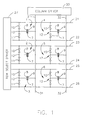
- FIG. 1 is a schematic circuit diagram of an AMLCD according to a first technical example.
- the AMLCD includes a plurality of pixels 1-6 arranged in a matrix array on the active substrate of the display.
- Pixel 1 includes liquid crystal layer 7 sandwiched between individual pixel electrode 8 and common electrode 9, as well as MIM diodes 10 and 11 which are coupled to one another and to pixel electrode 8 via common node 12.
- Common node 12 is in communication with each of MIM diodes 10, 11, via branches extending therefrom, as well as with pixel electrode 8.
- Each of the other pixels 2-6 also includes a pair of MIM diodes 10, 11 coupled at a common node 12, as well as LC material 7 sandwiched between pixel electrodes 8 and 9.
- the common electrode 9 in each pixel is in electrical communication with a column or data line 31, 32.
- the Figure 1 display further includes row or select lines 21-26 that are driven and selected by row select driver 27, and column or data lines 31 and 32 which are selected and driven by column driver 33.
- Select lines 21-26 are all substantially parallel to one another and are oriented in a first direction, while data lines 31-32 are also substantially parallel to one another, but are oriented in a second direction that is substantially orthogonal to the first direction.
- select lines 21-26 are substantial orthogonal to data lines 31-32 across the active matrix array.
- a pair of row or select lines is provided for each pixel, while only a single column or data line is utilized for each pixel.
- the AMLCD includes additional pixels as well as additional select and data address lines sufficient in number so as to form a usable image for displaying to a viewer (e.g. see Figure 6 ).
- Each of the pixels 1-6 herein is substantially identical.
- the insulator in MIM diodes 10-11 is conventionally either anodized Ta 2 O 5 (tantalum oxide) or Si-rich SiN x (silicon nitride) grown by plasma enhanced chemical vapor deposition (CVD).
- SiN x diodes have steeper current voltage characteristics than Ta 2 O 5 diodes and a lower diode capacitance. Thus, SiN x diodes are more attractive for higher resolution displays.
- SiN x diodes suffer from device degradation and spacial non-uniformity.
- the pixel circuits described herein thus are designed so as to have greatly increased tolerance for spacial and temporal variations of MIM diode current-voltage characteristics, as SiN x MIM diodes are preferred.
- a row of pixels (e.g. pixels 1 and 4) is selected by applying simultaneously opposite polarity pulses to select lines 21 and 22 while at the same time applying data voltage to the column lines in that particular row as desired.
- the polarity of the voltage pulses on any given select line remain constant for that line. In other words, on select line 21, for example, the polarity of pulses thereon will always be positive while the polarity of the pulses on the corresponding select line 22 will always be negative. This allows for less complex circuitry to be utilized. This is the case with all pixels disclosed herein.
- SiN x MIM diodes are utilized in this third embodiment.
- Two MIM diodes are connected to each LC pixel, and two separate select lines (21 and 22 for pixel 1).
- a row of pixels is selected by applying simultaneously opposite polarity pulses 41 and 42 of substantially equal magnitude, to the pixel, while applying data voltage to the corresponding column line 31.
- SiN x MIM diodes 10-11 any variation in the current-voltage characteristic of the MIM device over time, with temperature, or across the display area will result in a variation of the LC voltage.
- the thickness and composition (i.e. Si/N ratio) of the SiN x layer determines in part the diode's current-voltage curve. Because it is difficult to control thickness and composition accurately over large area, the current voltage curve of such SiN x MIM diodes 10-11 will vary significantly across large area displays.
- the SiN x diode current decreases, when pulsed in the on-state for an extended period of time, leading to image retention in conventional circuits.
- MIM current also depends on temperature, a non-uniform heating of the display will result from pixel voltage variation across the display area. Circuits herein overcome these problems.
- a select voltage 41 of about 15 volts is applied to select line 21, while simultaneously a select voltage 42 of -15 volts is applied to select line 22, while a data voltage of 5 volts is applied to column or data line 31.
- These voltages may range from 10-30 volts for line 21, and from -10 to -30 for line 22.
- the 4(a) circuit of pixel 1, when these signals are applied, the pixel charging saturates rapidly at the data voltage and is virtually independent of MIM current variations up to 10X.
- the pixel charging saturates quickly, because the voltage across each MIM device 10, 11 is still 15 volts when the pixel voltage approaches the data voltage, so that a significant on-current keeps flowing until the select pulses are switched off.
- the pixel voltage shift at termination of the select pulses 41 and 42 is substantially eliminated in the illustrated circuit, because the capacitive feed through voltage of diodes 10-11 substantially cancels out.
- the illustrated Figure 4(a) circuit can still charge the pixel almost completely.
- Figures 1 and 2(a)-2(b) While the third example shown in Figures 4(a)-4(b) , when operated in a simultaneous scan mode, has numerous advantages over prior art MIM LCD technology including much improved spacial and temporal gray shade control and uniformity, faster response time, reduced image retention and cross-talk, and increased tolerance for RC delays on the row and column lines, the drawback of the Figure 4(a)-4(b) arrangement is that it needs to have at least a ten volt swing on the data line in order to obtain sufficient voltage across LC 7 and the relatively high voltage that can occur across MIM diodes in the off-state (during the non-select period).
- V D varies between -2.5 and +2.5 volts in this example
- V S may range from about 10-30 volts
- V offset may range from about 2-4 volts.
- the maximum voltage across each MIM diode 10, 11 in the off-state is about 7 to 8 volts, resulting in improved charge retention in the LC 7 capacitance in each pixel.
- the cancellation of the pixel voltage shift from the two diodes is not complete in this drive scheme, because the opposite polarity pulses on lines 21 and 22, for example, are not of equal magnitude.
- the data voltage is applied in row inversion mode [i.e. the data signal voltage polarity is charged for each row].
- pixel 1 is driven as follows.
- a pulse of V S - V offset (e.g. 15 volts - 3 volts equals 12 volts) is applied to select line 21, while a pulse of -V S - V offset (e.g. -15 volts - 3 volts equals -18 volts) is simultaneously applied to select line 22, while at the same time a data voltage of 2.5 volts is applied to column line 31.
- a 30 volt differential is applied between select lines 21 and 22, after each select pulsing, each node branch has a drop of 15 volts.
- node 12 When MIM diodes 10-11 are switched off, node 12 floats and follows the column line voltage so that, for example, if -2.5 volts are applied to column line 31, the voltage at node 12 goes to -8 volts, while select line 21 and 22 are at 0 volts.
- the circuit enables the system to use less voltage on the column lines (this saves cost and circuit complexity), and allows less voltage variation at both node 12 and on the column lines so that there is less leakage through MIM diodes 10 and 11. Minimizing leakage through diodes 10-11 in the MIM off-state is desirable as will be appreciated by those of skill in the art.
- a voltage of V S + V offset (e.g. 15 volts + 3 volts equals 18 volts) is applied to select line 21, while a voltage of -V S + V offset (-15 volts + 3 volts equals -12 volts) is applied to select line 22, while a data voltage is applied to column line 31.
- the signal on line 21 goes back to V S - V offset and the signal on line 22 goes back to -V S - V offset for the next pulsing.
- the pulsing on each of lines 21 and 22 alternate between these two values for subsequent frames when the AMLCD is on.
- Each pixel in the active matrix array is driven in a similar manner.
- the Figure 2(a)-2(b) arrangement allows the circuit to have a smaller voltage swing on the data line (i.e. column line 31), while still obtaining sufficient voltage across liquid crystal material 7 in each pixel and limiting leakage through the MIM diodes 10-11.
- the voltage swing on line 31 is reduced to 5 volts (from 2.5 volts to -2.5 volts) which is an improvement over the 10 volt swing shown in Figure 4(a) .
- the Figure 2(a)-2(b) embodiment has a reduced number of voltage levels applied to the select lines, than does the prior art discussed in the Background Section of this application.
- the voltage drop on the column or data lines is no greater than about 6 volts, preferably less than or equal to about 5 volts, while the voltage swing between corresponding select lines is no greater than about 32 volts, and is preferably less than or equal to about 30 volts.
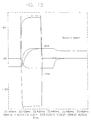
- FIGS 5-6 illustrate an embodiment of this invention, where, in contrast to the first three examples discussed above, a pair of separate MIM diodes are provided in each node branch. Therefore, we have four MIM diodes per pixel.
- This design improves the symmetrical nature of the circuit, and results in improved driving characteristics when, as discussed above, the pulse signals on each select line always have the same polarity.
- twin MIM diodes 10, 11, connected back-to-back in each branch the pixel voltage on pixel electrode 8, and at common node 12, goes exactly to: (V 1 + V 2 ) ⁇ 2, at the end of the select time, wherein V 1 is the voltage pulse on line 21 and V 2 is the voltage pulse on line 22. This is perfectly symmetrical.
- Figure 6 is a top view illustrating a matrix array of pixel electrodes 8, select lines 21, 22, and MIM diodes 10, 11, according to the Figure 5 embodiment of this invention.
- This Figure 5-6 embodiment may use the drive schemes in any of the other embodiments of this invention (e.g. see Figures 2(b) -4(b) ).
- FIG. 8 Each of the above discussed and/or illustrated examples or embodiments is compatible with row inversion (e.g. Fig. 8 ) and frame inversion (e.g. Fig. 7 ) types driving schemes for LCD applications. This is in contrast to the Maeda '728 patent which, unfortunately, is limited to frame inversion applications. Additionally, the Figure 4(a) and 4(b) arrangement discussed above is compatible with both column inversion driving and pixel inversion driving. Center return video (e.g. 10 to 14 volt data driver) is typically used with the Fig. 4(a) -4(b) arrangement, while bipolar video (e.g. 5 volt data driver) is typically used with other embodiments and examples.
- Center return video e.g. 10 to 14 volt data driver
- bipolar video e.g. 5 volt data driver
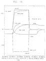
- Figure 7 shows frame inversion, as all of the pixels in the display have the same polarity (+ or -) during a given frame, and the polarity of each pixel is changed for subsequent frames. Two frames, one after the other, are shown in Figure 7 .
- Frame inversion is undesirable in that it leads to top-to-bottom shading, cross talk, and flicker in LCD applications and is therefore almost never used.
- Flicker is typically defined by variation in luminance of more than a certain percentage (e.g. 5-10%) at frequency less than about 40 Hz. Because flicker can be reduced by spatial averaging, the solution to the flicker problems associated with frame inversion are row inversion, column inversion, and/or pixel inversion described below.
- Figure 8 shows an example of row inversion, where one row of pixels in the display has a "+" polarity for an entire frame and another adjacent row of pixels has an opposite "-" polarity during that frame.
- each row of pixels alternates polarity in each frame, and the polarity in each pixel changes for each frame so that if a pixel is "+" in one frame, it will be "-" in the next frame (this is the case for the illustrated examples of Figs. 7-10 herein).
- Two frames, one after the other, are shown in Fig. 8 .
- every other row is of the same polarity so that adjacent rows in a given frame are of opposite polarity.
- adjacent rows may be of the same polarity (e.g. where the first and second rows are "+”, the third and fourth rows “-”, the fifth and sixth rows “+”, etc.
- row inversion reduces flicker due to spatial averaging, and reduces vertical cross talk. All MIM examples or embodiments may be driven using these row inversion techniques, as they are preferable.
- Figure 9 illustrates column inversion, which reduces flicker and horizontal cross talk.
- the Figure 4(a)-4(b) arrangement may utilize column inversion driving techniques.
- each column of pixels in the LCD has the same polarity in a given frame, and then switches polarity for the next frame.
- adjacent columns of pixels in a given frame have opposite polarities "+" and "-".
- Figure 10 illustrates pixel or dot inversion, which results in high image quality due to reduction in vertical and horizontal cross talk.
- Pixel or dot inversion is impossible with a pixel having only one MIM in it (i.e. a single MIM circuit).
- Pixel inversion can only be done in a pixel having at least two MIMs, such as in the instant dual MIM circuit having two select lines per pixel. Flicker is also reduced with pixel inversion.
- the Fig. 4(a)-4(b) arrangement may utilized pixel or dot inversion. Again, the polarity of each pixel changes from frame to subsequent frame, and all pixels of the display in a given frame are not of the same polarity (this is also the case with row and column inversion).
- polarity is defined as the polarity of the voltage at the pixel node V p (or 12) with respect to the voltage on the opposite electrode 9 across the LC layer 7.
- the opposite electrodes 9 across the display are made up of patterned columns of ITO or the like to which data signals are applied.
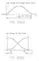
- bipolar video ( Figure 20(b) )
- ON and OFF state of the pixel are respectively, e.g. +2.5 volts and -2.5 volts during the first frame, and -2.5 volts and +2.5 volts during the second frame, etc.
- the additional voltage needed to fully turn on the LC comes from biasing the node 12 between the two MIM diodes to e.g. -3 V and +3 V respectively during first and second select times.
- the polarity of data for ON and OFF state and polarity for bias at the node 12 are simply reversed to obtain row inversion.
- center return video ( Fig. 20(a) )
- the OFF state is 0 V and the ON state is +5 V and -5 V during first and second frames, respectively, and the voltage applied to the node 12 between the MIM diodes during the select time can stay at zero at all times.
- SSDM simultaneous scan dual MIM
- SSDM simultaneous scan dual MIM
- the SSDM arrangements are substantially insensitive to variations in MIM characteristics as to RC delays on rows as well as column as will be further discussed below.
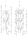
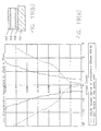
- circuit simulations shown in Figs. 11 and 12 of 28 inch diagonal SVGA displays were performed.
- Figure 11 is a circuit simulation of one row of a conventional single MIM LCD
- Figure 12 is a circuit simulation of one row of pixels of a SSDM LCD according to the discussed examples.
- the Figure 12 SSDM device is superior relative to the single MIM Figure 11 device. Certain simulation parameters used in both the Fig. 11 and Fig.
- FIG. 11 and 12 show the Pspice simulation circuit for the single and dual MIM displays, respectively.
- An exponential model is a fairly good representation of the actual measured curves and is easy to implement in Pspice.
- a more accurate physics/based model for the conduction mechanism is Frenkel-Poole conduction.
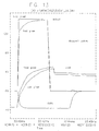
- Figures 13-18 were obtained from the Figure 11-12 simulations.
- Figures 15 and 16 show the same curves for the SSDM circuit of Figure 12 . Note the differences between the single MIM graphs of Figs. 13-14 and the dual MIM graphs of Figs. 15-16 .
- Fig. 17 shows a three dimensional plot of the pixel voltage variation of the Fig. 11 circuit
- Fig. 18 shows a three dimensional plot of the pixel voltage variation of the Fig. 12 circuit, with each of Figs.
- V pix V pix , - + Ts ⁇ 0 I mim [V mim (t)]dt/C lc , where V pix , - is the pixel voltage immediately before the select pulse, Ts is the select time, I min is the MIM current which depends on the MIM voltage V mim , and C lc is the capacitance of the LC or liquid crystal material in the pixel.
- V mim (t) V select (t) -V data (t) -V lc (t).
- V mim (t) V select (t) -V data (t) -V lc (t).
- the above two equations show that the pixel voltage V pix depends on the initial pixel voltage V pix , - , on the MIM current-voltage characteristics, on Clc (which in turn depends on voltage, time and cell gap of the lc), and also on the detailed shapes of the select pulse and data pulse. In other words, select and data pulse distortion along the buslines or address lines will have a substantial effect on the pixel voltage. This is clear from the charging plots for the single MIM circuit in Figs. 13 and 14 .
- the pixel voltage V pix is independent of the detailed MIM IV curves (i.e. current/voltage curves) and independent of the detailed shape of the select and data pulse, as long as pixel charging saturates.
- the IV curves of the two branches in the SSDM circuit e.g. see Figs. 1-5 which illustrate the two MIM branches in each pixel
- the dual MIM switch functions as an analog switch, when operated in a simultaneous select mode as illustrated herein, and transfers the data voltage exactly to the pixel, much like a TFT.
- Pixel charging saturates better in the dual MIM switch than in a TFT, because the switch current in the dual MIM circuit herein remains relatively high when the pixel voltage approaches the data voltage, whereas in a TFT the current goes to zero when the pixel voltage approaches the data voltage (i.e. when the source/drain voltage goes to zero).
- the pixel voltage shift, proportional to C mim /C lc in the single MIM circuit is absent in the dual MIM circuit due to cancellation of the capacitive feedthrough in the two branches.
- V pix V data
- Condition (a) is met because of the proximity of the MIM diodes in the two branches of one pixel.
- a SiN x diode IV curves can vary across the display area as a result of temperature variations, SiN x thickness and composition (e.g. Si/N ratio) variations or dimensional variations in the MIM area, they can be normally assumed not to vary over a few hundred microns within a pixel.
- Condition (b) may require the two select voltages to have equal magnitudes across the entire display.
- the load on the rows in the SSDM circuit has both a capacitive and a resistive component (as compared to TFT arrays, where the load is purely capacitive as long as the gate nitride is not leaky).
- a row resistance of e.g. 2 kohm gives good uniformity in the 28 in.
- Dual MIM SVGA display and corresponds to an A1 (aluminum) row busline with a width of 30 ⁇ m and a thickness of 0.3 ⁇ m.
- the row line metal is the last metal deposited and functions also as the top electrode for the MIM diode in the current process in certain embodiments.
- a thicker A1 layer of e.g. 1 ⁇ m makes even larger displays feasible.
- amorphous C:N (carbon nitride) alloy film is used as the insulator or semi-insulator of each MIM diode 10, 11.
- This insulator (or semi-insulator) 104 is typically located between two opposing electrodes of the TFD or MIM diode, as shown in Fig. 19(b) .
- a MIM or TFD diode, invented herein, including a-C:N as the semi insulator, has current voltage characteristics which are desirable for a switch in a metal-insulator-metal (MIM) LCD display or x-ray imaging device.
- MIM metal-insulator-metal
- This a-C:N alloy is a material that emulates its crystalline component beta-CN. The latter has a hardness value greater than that of diamond and is very stable to heat, light, and electrical stress.
- the high field electrical conduction of a-C:N has been studied over a temperature range of 300-500K, and current is found to increase exponentially with the electric field.
- the exponential factor is found to increase linearly with the inverse of temperature in this range.
- the activation energy of the conductivity is also found to be strongly field dependent and to increase linearly with electric field.
- a-C:N thin films show I-V characteristics with higher gradient than Si-rich Si x N y of comparable thickness.
- a-C:N does not show any substantial photoconductivity even at light photons with energies larger than its bandgap of about 2.4 eV.
- the electrical relative permittivity is about 3-4. This means that MIM devices 10, 11 with larger area can be fabricated hence the use of a scanning projector for large 2D array fabrication, instead of more expensive aligners.
- the alloy may include or consist essentially of on carbon (C), nitrogen (N), and hydrogen (H).
- C carbon
- N nitrogen
- H hydrogen
- in the alloy from about 20-60% of the atoms in the alloy are nitrogen atoms (more preferably from about 40-60%)
- from about 40-80% of the atoms in the alloy are carbon atoms (more preferably from about 40-60%)
- hydrogen, which is optional is provided in the alloy from about 0-25% of the atoms in the alloy are hydrogen atoms (more preferably from about 0-15%, and most preferably from about 1-5%).
- a-C:N films with the above characteristics can be synthesized at low substrate temperatures ( ⁇ 100 degrees C) by two techniques: (i) growth from solid carbon, and (ii) growth from gas phase. Growth from solid carbon - sputtering of graphite targets by Ar+ ions with simultaneous low energy (e.g. from about 100-500 eV) N+ peening or assisted bombardment at ion beam densities of approximately 0.5 mA/cm 2 . These conditions are favorable for the growth of a-C:N films with relatively high N/C atomic ratios from about 0.4 to 0.6.
- the use of electron energy loss spectroscopy initially shows that while the carbon was hybriseed tetrahedrally the nitrogen was sp2 hybridised giving unpolarized covalent C-N bonds. Further electron diffraction studies show that the films have a nano crystals of beta-C-N embedded in an essentially amorphous matrix.
- the films show hardness of about 60 Gpa and electrical resistivity of above 7 x 10 12 ohm-cm.
- the alloy has an electrical resistivity of from about 5 x 10 7 to 7 x 10 12 .
- the optical bandgap was above 3 eV, and in certain examples the alloy's Tauc bandgap is at least about 3.0.
- the alloy has a hardness of at least about 50 Gpa, and more preferably of at least about 70 Gpa.
- the films can be deposited using a plasma enhanced CVD (chemical vapor deposition) method in which acetelyne and NF 3 /NH 3 gas mixtures are introduced into a chamber via separate gas lines.
- the power density ⁇ 500 W/m 2 and substrate temperature ⁇ 350K.
- nitrogen incorporation into the carbon matrix causes a reduction in the bandgap of the carbon network.
- CF 4 /O 2 as an etchant gas may be used.
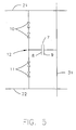
- FIG. 19(b) shows a TFD (e.g. MIM diode 10, 11) on substantially transparent glass substrate 101 according to another example.
- this TFD may be a MIM diode 10, 11 wherein bottom electrode 102 and top electrode 103 are both of metals (e.g. Mo) while insulator or semi-insulator layer 104 disposed therebetween is of a material such as a-C:N as discussed above.
- a non-metal such as indium-tin-oxide (ITO) may be used as one or both of the electrode(s) 102/103 in the diode of Fig. 19(b) .
- ITO indium-tin-oxide
- the TFD includes ITO as bottom electrode 102 and Mo as top electrode 103, with either diamond-like carbon, a-C:N, or silicon rich liquid nitride as semi-insulator 104.
- MIM diodes are nonlinear resistance elements.
- the liquid crsytal is sealed between two opposing substrates on which column and row lines are formed, respectively, and the nonlinear resistance elements (e.g. MIMs) and one set of pixel electrodes are formed on the inner surface of one of the substrates 101.
- the other pixel electrode, opposite the pixel electrode formed on substrate 101, is formed on an opposing substrate on the other side of the LC layer as shown in U.S. Pat.
- the non linear resistance diodes 10, 11 are electrically connected between one of the pixel electrodes and the select lines on substrate 101. It is noted that in nonlinear resistance elements, a very small current flows even during the retention period, so that stored data is affected gradually by data signals.
- layer 104 of TFD (e.g. MIM diode) 10, 11 of Fig. 19(b) may be of nanocrystalline carbon, or of polycrystalline carbon.
- Semi-insulators of MIM or TFD diodes have typically been of Ta 2 O 5 or PECVD grown Si-rich SiN x :H.
- a drawback of these two materials is their relatively high dielectric constant values: about 23 and 8.5 respectively for Ta 2 O 5 and SiN x :H, respectively.
- these electronic materials being binary and ternary alloys, are prone to issues such as spatial homogeneity and temporal degradation when used within an active device such as a diode in this case.
- the simultaneous scan dual TFD or MIM [SSDM] approach shown and discussed above in Figs. 1-10 , 12 , 15 , 16 , 18 , 19(b) , and 20 is/are provided in order to overcome the effects of spatial, temporal, and temperature dependent variations in TFD and MIM device characteristics.
- I-V symmetry or symmetricity of the TFD or MIM devices 10, 11 should be good. Symmetry can be achieved by using two diodes in series per branch as shown in Fig. 5 for example. This approach however implies that the switching voltage needed per pixel is doubled and consequently is at the fringe of operability of presently available drivers.
- the present example uses semi-insulators in the form of poly-crystalline diamond and nanocrystalline carbon thin films optionally containing small amounts of N and F dopant atoms for TFD or MIM semi-insulator layer 104 [see Fig. 19(b) ]. Additional desirable features of these two films include (i) low dielectric constant of less than about 4.0, preferably between about 3.0 and 4.0, which implies a lower capacitive coupling and kickback voltage; (ii) wide bandgap E diamond of approximately 5.3-5.7 eV, preferably aboaut 5.5 eV, and E dlc >3eV, which results in high transparency and virtually no photoconductivity because the density of states (DOS) is above 10 18 cm -3 eV -1 pinning the Fermi-Level in the gap; (iii) high dielectric breakdown strength E > 5 x 10 6 V cm -1 ; (iv) highly symmetric I-V (current-voltage) characteristics requiring half of the switching voltage needed for Si-rich SiN
- a MIM or TFD can be made by providing a substrate 101 such as glass, depositing and patterning a first electrode 102 array (e.g.
- MIM or TFD devices 10, 11 can be made in accordance with this invention.
- MIM and TFD diodes 10, 11 herein are non-linear resistance elements, and are also bi-directional threshold devices.
- Figure 19(a) is a voltage versus current (amps) graph illustrating I-V characteristics of a carbon MIM (solid line) versus a a-Si:N MIM (dotted line). Note the low variation of voltage as a function of current for the carbon MIM diode of Fig. 19(a) .
Landscapes
- Engineering & Computer Science (AREA)
- Chemical & Material Sciences (AREA)
- Crystallography & Structural Chemistry (AREA)
- Physics & Mathematics (AREA)
- Computer Hardware Design (AREA)
- General Physics & Mathematics (AREA)
- Theoretical Computer Science (AREA)
- Liquid Crystal (AREA)
- Liquid Crystal Display Device Control (AREA)
- Control Of Indicators Other Than Cathode Ray Tubes (AREA)
Claims (10)
- Ein Verfahren zum Adressieren eines Flüssigkristalldisplays mit Filmdioden, wobei das Flüssigkristalldisplay umfasst eine Vielzahl von Pixeln (1-6) in dem Display, wobei jedes Pixel enthält: eine Flüssigkristallschicht (7) und ein Paar von Elektroden (8,9), welche einen Kondensator bilden; erste und zweite MIM-Dünnfilmreihendiodenpaare (10,11), die über einen gemeinsamen Knotenpunkt (12) miteinander gekoppelt sind, wobei der gemeinsame Knoten (12) angeordnet ist zwischen a. dem Reihendiodenpaaren und b. dem Kondensator; und mit ersten und zweiten Auswahladressierleitungen (21,22) und eine Datenadressierleitung (31,32), wobei die erste Auswahladressierleitung (21) an dem ersten Reihendiodenpaar (10) angekoppelt ist und wobei die zweite Auswahladressierleitung (22) an dem zweiten Reihendiodenpaar (11) angekoppelt ist; mit den Verfahrensschritten:Vorspannen der ersten (10) und zweiten (11) Reihendiodenpaare in einen Zustand, um das Abspeichern von Ladung in dem Kondensator von dem Pixel durch Variieren einer Auswahlspannung zu ermöglichen, die an einer ersten Auswahladressierleitung (21) zwischen Vs + Voffset und Vs - Voffset für einander folgende Rahmen und durch Variieren einer Auswahlspannung, die an der zweiten Auswahladressierleitung (22) zwischen -Vs + Voffset und -Vs - Voffset für einander folgende Rahmen angelegt wird, wobei die Stärke von Vs größer als die Stärke von Voffset ist, die größer als Null ist; wobei die Polarität für Vs + Voffset und Vs - Voffset Pulse immer positiv in einander folgenden Rahmen ist, und worin die Polarität für -Vs + Voffset und -Vs - Voffset Pulse immer negativ in einander folgenden Rahmen ist.
- Das Verfahren nach Anspruch 1, des Weiteren enthaltend das Anlegen an einem Rahmen von Vs - Voffset an die erste Auswahladressierleitung (21) bzw. Anlegen von -Vs - Voffset an die zweite Auswahlleitung (22) zum selben Zeitpunkt und Anlegen von Vs + Voffset an die erste Auswahlleitung (21) und von -Vs + Voffset an die zweite Auswahlleitung (22) zur gleichen Zeit in einem folgenden Rahmen.
- Das Verfahren nach Anspruch 1, dadurch gekennzeichnet, dass alle Operationspotentiale, die an die erste Auswahlleitung (21) angelegt werden, eine positive Polarität aufweisen und alle Operationspotentiale, die an eine zweite Auswahlleitung (22) angelegt werden, eine negative Polarität aufweisen.
- Das Verfahren nach Anspruch 1, des Weiteren umfassend das Aufrechterhalten einer im wesentlichen konstanten Spannungslücke zwischen den Potentialen, die an die erste (21) und an die zweite (22) Auswahlleitungen in allen Rahmen während der Nichtauswahlperioden angelegt wird.
- Das Verfahren nach Anspruch 1, des Weiteren enthaltend die Verfahrensschritte: Anlegen von Haltespannungen an jede der ersten (21) und zweiten (22) Auswahlleitungen während der Nichtauswahlperioden, um die Halteladung in den Pixeln zu verbessern.
- Das Verfahren nach Anspruch 5, des Weiteren umfassend das Aufrechterhalten der Haltespannungen in den ersten (21) und zweiten (22) Auswahlleitungen während der vollständigen Nichtauswahlperiode zwischen Pulsen, um so von den ersten (10) und zweiten (11) Diodenpaaren eine Spannungsverschiebung auszulöschen.
- Das Verfahren nach Anspruch 6, des Weiteren umfassend, dass bei der Beendigung der Datenspannungspulse die Spannungen an den ersten und zweiten Auswahlleitungen mit gleicher Größe aber entgegengesetzter Polaritätsmenge geändert werden, um so die Haltespannungen zu implementieren.
- Ein Pixel für ein Flüssigkristalldisplay, wobei das Pixel enthält:einen Kondensator, der von einer Flüssigkristalllage (7) ausgebildet ist, die zwischen ersten (8) und zweiten (9) Elektroden zwischengelegt ist;erste und zweite (10,11) MIM-Dünnfilmreihendiodenpaare (TFDs) ;einen Knotenpunkt (12), der folgendes zusammenkoppelt, (i) das erste Reihendiodenpaar, (ii) das zweite Reihendiodenpaar und (iii) diesen Kondensator;erste (21) und zweite (22) parallel geschaltete Auswahlleitungen, wobei die erste Auswahlleitung (21) an diesem ersten Reihendiodenpaar (10) angeschlossen ist und wobei diese zweite Auswahlleitung (22) an dieses zweite Reihendiodenpaar (11) angeschlossen ist;wobei die Auswahlleitungen (21,22) an entgegengesetzten Elektroden von dem Diodenpaar angeschlossen sind, wenn das eine an die Flüssigkristalldiode angeschlossen ist;eine Datenleitung (31,32), die senkrecht zu den ersten (21) und zweiten (22) Auswahlleitungen ausgerichtet ist;Antriebsmittel, die simultan den Versatz abtasten, um das Pixel zu laden, um so Daten an einem Zuschauer des Displays zur Verfügung zu stellen, wobei die Simultanversatz-Abtastantriebsmittel für simultanes Anlegen in einem ersten Rahmen eine Auswahlspannung von Vs + Voffset an die erste Auswahlleitung (21) und eine Auswahlspannung Vs -Vs - Voffset an die zweite Auswahlleitung (22) anlegen, und daraufhin simultanes Anlegen an einen zweiten Rahmen, der dem ersten Rahmen folgt, eine Auswahlspannung von Vs + Voffset an die erste Auswahlleitung (21) und eine Auswahlspannung von -Vs + Voffset an die zweite Auswahlleitung anlegen;worin die Stärke von Vs größer ist als die Stärke von Voffset , die größer als Null ist;wobei die Polarität für Vs + Voffset und Vs - Voffset Pulse immer positiv ist in einander folgenden Rahmen und worin die Polarität von -Vs + Voffset und -Vs - Voffset Pulsen immer negativ in einander folgenden Rahmen ist;
- Das Display gemäß Anspruch 8, des Weiteren enthaltend Mittel zum Anlegen einer Haltespannung an jeden dieser ersten (21) und zweiten (22) Auswahlleitungen zwischen Pulsen.
- Das Verfahren gemäß Anspruch 1, des Weiteren enthaltend das Antreiben des Displays über eine von a. Reiheninversion, b. Zeileninversion und c. Pixelinversion, so dass in einem gegebenen Rahmen eine erste Gruppe von Pixeln in dem Display eine erste Polarität aufweisen und eine zweite Gruppe von Pixeln in dem Display eine zweite Polarität aufweist, wobei die erste Polarität und die zweite Polarität einander entgegengesetzt sind, wobei die Polarität definiert ist im Hinblick auf eine Spannung an einem gemeinsamen Knotenpunkt relativ zu einer Spannung an der zweiten Pixelelektrode in einem bestimmten Pixel, so dass in dieser ersten Gruppe von Pixeln in diesem gegebenen Rahmen Spannung an dem gemeinsamen Knotenpunkt größer als die Spannung an der zweiten Pixelelektrode ist, und wobei in dieser zweiten Gruppe von Pixeln in diesem gegebenen Rahmen die Spannung an dem gemeinsamen Punkt kleiner ist, als die Spannung in der zweiten Pixelelektrode.
Applications Claiming Priority (4)
| Application Number | Priority Date | Filing Date | Title |
|---|---|---|---|
| US935678 | 1997-09-23 | ||
| US08/935,678 US6225968B1 (en) | 1997-09-23 | 1997-09-23 | Method and system for addressing LCD including diodes |
| US35819 | 1998-03-06 | ||
| US09/035,819 US6243062B1 (en) | 1997-09-23 | 1998-03-06 | Method and system for addressing LCD including thin film diodes |
Publications (3)
| Publication Number | Publication Date |
|---|---|
| EP0910062A2 EP0910062A2 (de) | 1999-04-21 |
| EP0910062A3 EP0910062A3 (de) | 1999-10-06 |
| EP0910062B1 true EP0910062B1 (de) | 2009-08-26 |
Family
ID=26712526
Family Applications (1)
| Application Number | Title | Priority Date | Filing Date |
|---|---|---|---|
| EP98117949A Expired - Lifetime EP0910062B1 (de) | 1997-09-23 | 1998-09-22 | Verfahren und Einrichtung zur Adressierung von Flüssigkristall-Anzeigetafeln mit Dünnfilm-Dioden |
Country Status (3)
| Country | Link |
|---|---|
| US (1) | US6243062B1 (de) |
| EP (1) | EP0910062B1 (de) |
| CA (1) | CA2246837C (de) |
Families Citing this family (39)
| Publication number | Priority date | Publication date | Assignee | Title |
|---|---|---|---|---|
| JPH1130975A (ja) * | 1997-05-13 | 1999-02-02 | Oki Electric Ind Co Ltd | 液晶表示装置の駆動回路及びその駆動方法 |
| US7304632B2 (en) * | 1997-05-13 | 2007-12-04 | Oki Electric Industry Co., Ltd. | Liquid-crystal display driving circuit and method |
| US6243062B1 (en) | 1997-09-23 | 2001-06-05 | Ois Optical Imaging Systems, Inc. | Method and system for addressing LCD including thin film diodes |
| KR100338007B1 (ko) * | 1997-09-30 | 2002-10-11 | 삼성전자 주식회사 | 액정 표시 장치 및 그의 구동 방법 |
| US6222596B1 (en) | 1998-03-06 | 2001-04-24 | Ois Optical Imaging Systems, Inc. | Thin film diode including carbon nitride alloy semi-insulator and method of making same |
| TW521241B (en) * | 1999-03-16 | 2003-02-21 | Sony Corp | Liquid crystal display apparatus, its driving method, and liquid crystal display system |
| US6563482B1 (en) | 1999-07-21 | 2003-05-13 | Semiconductor Energy Laboratory Co., Ltd. | Display device |
| US6469684B1 (en) * | 1999-09-13 | 2002-10-22 | Hewlett-Packard Company | Cole sequence inversion circuitry for active matrix device |
| CN1636163A (zh) * | 2001-06-20 | 2005-07-06 | 赛特勒有限公司 | 薄平面开关及它们的发明应用领域 |
| KR100917324B1 (ko) * | 2002-11-16 | 2009-09-11 | 엘지디스플레이 주식회사 | 모바일 폰용 액정표시장치 |
| KR100920355B1 (ko) * | 2003-03-28 | 2009-10-07 | 삼성전자주식회사 | 액정 표시 장치용 박막 다이오드 표시판 및 이를 포함하는액정 표시 장치 |
| US20050083283A1 (en) * | 2003-10-17 | 2005-04-21 | Scanvue Technologies Llc | Differentiating circuit display |
| KR100951359B1 (ko) * | 2003-10-29 | 2010-04-09 | 삼성전자주식회사 | 박막 다이오드 표시판 및 그 제조 방법 |
| KR100925471B1 (ko) * | 2003-10-29 | 2009-11-06 | 삼성전자주식회사 | 반투과형 액정 표시 장치용 박막 다이오드 표시판 |
| KR100961960B1 (ko) * | 2003-11-18 | 2010-06-08 | 삼성전자주식회사 | 액정 표시 장치, 박막 다이오드 표시판 및 그 제조 방법 |
| KR101026802B1 (ko) * | 2003-11-18 | 2011-04-04 | 삼성전자주식회사 | 액정 표시 장치 및 그 구동 방법 |
| JP2005156764A (ja) * | 2003-11-25 | 2005-06-16 | Sanyo Electric Co Ltd | 表示装置 |
| US6967118B2 (en) * | 2004-03-09 | 2005-11-22 | Hewlett-Packard Development Company, L.P. | Process for creating Metal-Insulator-Metal devices |
| US20050225543A1 (en) * | 2004-04-07 | 2005-10-13 | Scanvue Technologies Llc | Display circuit having asymmetrical nonlinear resistive elements |
| TWI282876B (en) * | 2004-10-07 | 2007-06-21 | Au Optronics Corp | TFD LED device with high aperture ratio |
| US20060091496A1 (en) * | 2004-10-28 | 2006-05-04 | Hewlett-Packard Development Company, Lp | Metal-insulator-metal device |
| US7160745B2 (en) * | 2004-10-28 | 2007-01-09 | Hewlett-Packard Development Company, L.P. | Metal-insulator-metal device |
| US8044882B1 (en) | 2005-06-25 | 2011-10-25 | Nongqiang Fan | Method of driving active matrix displays |
| KR101244656B1 (ko) * | 2006-06-19 | 2013-03-18 | 엘지디스플레이 주식회사 | 액정표시장치 |
| US7969276B2 (en) * | 2007-04-25 | 2011-06-28 | Scanvue Technologies, Llc | Thin film varistor array |
| US9570004B1 (en) * | 2008-03-16 | 2017-02-14 | Nongqiang Fan | Method of driving pixel element in active matrix display |
| US20120081347A1 (en) * | 2010-09-30 | 2012-04-05 | Apple Inc. | Low power inversion scheme with minimized number of output transitions |
| US8698723B1 (en) * | 2011-09-05 | 2014-04-15 | Nongqiang Fan | Method of driving active matrix displays |
| US8674918B1 (en) * | 2011-09-05 | 2014-03-18 | Nongqiang Fan | Method of driving active matrix displays |
| US8941640B2 (en) | 2012-06-08 | 2015-01-27 | Apple Inc. | Differential VCOM resistance or capacitance tuning for improved image quality |
| CN103236496B (zh) * | 2013-04-18 | 2015-08-12 | 福州大学 | 一种叠层结构的三端有源器件 |
| CN107924094B (zh) | 2015-07-24 | 2020-10-30 | 俄勒冈州立大学 | 使用非晶态金属非线性电阻器作为有源子像素器件的面内切换液晶显示器背板 |
| JP2021520060A (ja) | 2018-03-30 | 2021-08-12 | アモルフィックス・インコーポレイテッド | アモルファス金属薄膜トランジスタ |
| US10634949B1 (en) * | 2018-10-17 | 2020-04-28 | a.u. Vista Inc. | Display systems and methods involving MIM diodes |
| US11138944B2 (en) * | 2018-12-06 | 2021-10-05 | Xianyang Caihong Optoelectronics Technology Co., Ltd | Pixel matrix driving device and display device |
| KR102737478B1 (ko) * | 2018-12-07 | 2024-12-03 | 아모르픽스, 인크 | 다이오드 기반 디스플레이 백플레인 및 전자 디스플레이를 위한 방법 및 회로 |
| US12075656B2 (en) | 2020-06-12 | 2024-08-27 | Amorphyx, Incorporated | Circuits including non-linear components for electronic devices |
| CN117116224B (zh) * | 2023-08-31 | 2026-01-09 | 长沙惠科光电有限公司 | 显示面板和显示装置 |
| CN121260121A (zh) * | 2025-12-03 | 2026-01-02 | 青岛信芯微电子科技股份有限公司 | 显示设备及设备控制方法 |
Family Cites Families (11)
| Publication number | Priority date | Publication date | Assignee | Title |
|---|---|---|---|---|
| NL8502663A (nl) | 1985-09-30 | 1987-04-16 | Philips Nv | Weergeefinrichting met verbeterde aansturing. |
| US4731610A (en) | 1986-01-21 | 1988-03-15 | Ovonic Imaging Systems, Inc. | Balanced drive electronic matrix system and method of operating the same |
| FR2605778B1 (fr) | 1986-10-24 | 1990-11-16 | Thomson Csf | Panneau de visualisation a cristaux liquides et procede d'inscription des donnees sur ce panneau |
| GB2217891A (en) | 1988-04-29 | 1989-11-01 | Philips Electronic Associated | Matrix display device |
| US5142390A (en) | 1989-02-23 | 1992-08-25 | Ricoh Company, Ltd. | MIM element with a doped hard carbon film |
| EP0434627A3 (en) | 1989-12-18 | 1991-10-23 | Ois Optical Imaging Systems, Inc. | Balanced drive symmetric mim diode configuration for liquid crystal displays and method of operating same |
| JP2630663B2 (ja) | 1990-03-09 | 1997-07-16 | セイコー電子工業株式会社 | 電気光学装置 |
| JPH04122982A (ja) | 1990-09-13 | 1992-04-23 | Seiko Instr Inc | 電気光学装置の駆動方法 |
| JPH09511783A (ja) * | 1995-01-13 | 1997-11-25 | フラット パネル ディスプレイ カンパニー(エフペーデー)ベスローテン フェンノートシャップ | 液晶表示装置 |
| JP3110980B2 (ja) * | 1995-07-18 | 2000-11-20 | インターナショナル・ビジネス・マシーンズ・コーポレ−ション | 液晶表示装置の駆動装置及び方法 |
| US6243062B1 (en) | 1997-09-23 | 2001-06-05 | Ois Optical Imaging Systems, Inc. | Method and system for addressing LCD including thin film diodes |
-
1998
- 1998-03-06 US US09/035,819 patent/US6243062B1/en not_active Expired - Lifetime
- 1998-09-08 CA CA002246837A patent/CA2246837C/en not_active Expired - Fee Related
- 1998-09-22 EP EP98117949A patent/EP0910062B1/de not_active Expired - Lifetime
Also Published As
| Publication number | Publication date |
|---|---|
| CA2246837A1 (en) | 1999-03-23 |
| US6243062B1 (en) | 2001-06-05 |
| EP0910062A2 (de) | 1999-04-21 |
| EP0910062A3 (de) | 1999-10-06 |
| CA2246837C (en) | 2007-01-16 |
Similar Documents
| Publication | Publication Date | Title |
|---|---|---|
| EP0910062B1 (de) | Verfahren und Einrichtung zur Adressierung von Flüssigkristall-Anzeigetafeln mit Dünnfilm-Dioden | |
| US6222596B1 (en) | Thin film diode including carbon nitride alloy semi-insulator and method of making same | |
| DE68920935T2 (de) | Flüssigkristall-Anzeigevorrichtung mit aktiver Matrix mit reduziertem Flimmern. | |
| US4747671A (en) | Ferroelectric optical modulation device and driving method therefor wherein electrode has delaying function | |
| CA2231386C (en) | Liquid crystal display matrix array employing ovonic threshold switching devices to isolate individual pixels | |
| EP0510606B1 (de) | Flüssigkristallanzeigevorrichtung | |
| EP0786151B1 (de) | Flüssigkristall-anzeigevorrichtung mit einem schwellwertschalter | |
| US6225968B1 (en) | Method and system for addressing LCD including diodes | |
| CN101109881A (zh) | 一种液晶显示面板及其制造方法 | |
| US5541747A (en) | Electro-optical device utilizing a liquid crystal having a spontaneous polarization | |
| US6083574A (en) | Aligning method of liquid crystal, process for producing liquid crystal device, and liquid crystal device produced by the process | |
| EP0479291B1 (de) | Verfahren und Einrichtung zum Steuern eines Flüssigkristallanzeigegeräts | |
| JP2816549B2 (ja) | 電気光学装置 | |
| EP0526076B1 (de) | Aktive Flüssigkristallanzeigevorrichtung vom Matrixtyp | |
| Baraff et al. | The optimization of metal—Insulator—Metal nonlinear devices for use in multiplexed liquid crystal displays | |
| DE69120564T2 (de) | Verfahren zur Ansteuerung eines ferroelektrischen Flüssigkristallelementes und ferroelektrische Flüssigkristallanzeige | |
| JP2990232B2 (ja) | 液晶電気光学装置 | |
| EP0692779B1 (de) | Verfahren zur Steuerung einer Anzeigetafel | |
| WO2005038762A1 (en) | Differentiating circuit display | |
| EP0461648B1 (de) | Nachbildfreie Matrix-Flüssigkristallanzeige mit Metall-Isolator-Metall-Elementen | |
| JPWO1994018600A1 (ja) | 非線形抵抗素子およびその製造方法ならびに液晶表示装置 | |
| JP3161707B2 (ja) | 電気光学装置 | |
| den Boer et al. | Dual Branch MIM Array Technology for Low‐Cost AMLCDs | |
| JP2578941B2 (ja) | アクティブマトリクス液晶表示装置の駆動方法 | |
| JPH05110100A (ja) | アクテイブマトリクス型液晶表示装置 |
Legal Events
| Date | Code | Title | Description |
|---|---|---|---|
| PUAI | Public reference made under article 153(3) epc to a published international application that has entered the european phase |
Free format text: ORIGINAL CODE: 0009012 |
|
| AK | Designated contracting states |
Kind code of ref document: A2 Designated state(s): DE FR GB NL |
|
| AX | Request for extension of the european patent |
Free format text: AL;LT;LV;MK;RO;SI |
|
| PUAL | Search report despatched |
Free format text: ORIGINAL CODE: 0009013 |
|
| AK | Designated contracting states |
Kind code of ref document: A3 Designated state(s): AT BE CH CY DE DK ES FI FR GB GR IE IT LI LU MC NL PT SE |
|
| AX | Request for extension of the european patent |
Free format text: AL;LT;LV;MK;RO;SI |
|
| 17P | Request for examination filed |
Effective date: 20000405 |
|
| AKX | Designation fees paid |
Free format text: DE FR GB NL |
|
| RAP1 | Party data changed (applicant data changed or rights of an application transferred) |
Owner name: GUARDIAN INDUSTRIES CORP. |
|
| 17Q | First examination report despatched |
Effective date: 20060421 |
|
| GRAP | Despatch of communication of intention to grant a patent |
Free format text: ORIGINAL CODE: EPIDOSNIGR1 |
|
| GRAS | Grant fee paid |
Free format text: ORIGINAL CODE: EPIDOSNIGR3 |
|
| GRAA | (expected) grant |
Free format text: ORIGINAL CODE: 0009210 |
|
| AK | Designated contracting states |
Kind code of ref document: B1 Designated state(s): DE FR GB NL |
|
| REG | Reference to a national code |
Ref country code: GB Ref legal event code: FG4D |
|
| REF | Corresponds to: |
Ref document number: 69841088 Country of ref document: DE Date of ref document: 20091008 Kind code of ref document: P |
|
| PLBE | No opposition filed within time limit |
Free format text: ORIGINAL CODE: 0009261 |
|
| STAA | Information on the status of an ep patent application or granted ep patent |
Free format text: STATUS: NO OPPOSITION FILED WITHIN TIME LIMIT |
|
| 26N | No opposition filed |
Effective date: 20100527 |
|
| REG | Reference to a national code |
Ref country code: NL Ref legal event code: SD Effective date: 20110608 Ref country code: GB Ref legal event code: 732E Free format text: REGISTERED BETWEEN 20110602 AND 20110608 |
|
| REG | Reference to a national code |
Ref country code: FR Ref legal event code: TP |
|
| REG | Reference to a national code |
Ref country code: DE Ref legal event code: R082 Ref document number: 69841088 Country of ref document: DE Representative=s name: 2K PATENTANWAELTE BLASBERG KEWITZ & REICHEL, P, DE |
|
| REG | Reference to a national code |
Ref country code: DE Ref legal event code: R082 Ref document number: 69841088 Country of ref document: DE Representative=s name: 2K PATENTANWAELTE BLASBERG KEWITZ & REICHEL PA, DE Effective date: 20110930 Ref country code: DE Ref legal event code: R082 Ref document number: 69841088 Country of ref document: DE Representative=s name: 2K PATENTANWAELTE BLASBERG KEWITZ & REICHEL, P, DE Effective date: 20110930 Ref country code: DE Ref legal event code: R081 Ref document number: 69841088 Country of ref document: DE Owner name: CHIMEI INNOLUX CORP., TW Free format text: FORMER OWNER: GUARDIAN INDUSTRIES CORP., AUBURN HILLS, MICH., US Effective date: 20110930 |
|
| REG | Reference to a national code |
Ref country code: FR Ref legal event code: PLFP Year of fee payment: 19 |
|
| PGFP | Annual fee paid to national office [announced via postgrant information from national office to epo] |
Ref country code: NL Payment date: 20160926 Year of fee payment: 19 Ref country code: GB Payment date: 20160927 Year of fee payment: 19 |
|
| PGFP | Annual fee paid to national office [announced via postgrant information from national office to epo] |
Ref country code: FR Payment date: 20160926 Year of fee payment: 19 |
|
| PGFP | Annual fee paid to national office [announced via postgrant information from national office to epo] |
Ref country code: DE Payment date: 20160928 Year of fee payment: 19 |
|
| REG | Reference to a national code |
Ref country code: DE Ref legal event code: R119 Ref document number: 69841088 Country of ref document: DE |
|
| REG | Reference to a national code |
Ref country code: NL Ref legal event code: MM Effective date: 20171001 |
|
| GBPC | Gb: european patent ceased through non-payment of renewal fee |
Effective date: 20170922 |
|
| PG25 | Lapsed in a contracting state [announced via postgrant information from national office to epo] |
Ref country code: NL Free format text: LAPSE BECAUSE OF NON-PAYMENT OF DUE FEES Effective date: 20171001 |
|
| REG | Reference to a national code |
Ref country code: FR Ref legal event code: ST Effective date: 20180531 |
|
| PG25 | Lapsed in a contracting state [announced via postgrant information from national office to epo] |
Ref country code: DE Free format text: LAPSE BECAUSE OF NON-PAYMENT OF DUE FEES Effective date: 20180404 Ref country code: GB Free format text: LAPSE BECAUSE OF NON-PAYMENT OF DUE FEES Effective date: 20170922 |
|
| PG25 | Lapsed in a contracting state [announced via postgrant information from national office to epo] |
Ref country code: FR Free format text: LAPSE BECAUSE OF NON-PAYMENT OF DUE FEES Effective date: 20171002 |