EP0909950A2 - Bauelement mit planarer Leiterbahn - Google Patents
Bauelement mit planarer Leiterbahn Download PDFInfo
- Publication number
- EP0909950A2 EP0909950A2 EP98117990A EP98117990A EP0909950A2 EP 0909950 A2 EP0909950 A2 EP 0909950A2 EP 98117990 A EP98117990 A EP 98117990A EP 98117990 A EP98117990 A EP 98117990A EP 0909950 A2 EP0909950 A2 EP 0909950A2
- Authority
- EP
- European Patent Office
- Prior art keywords
- platinum
- conductor track
- component according
- alloy
- substrate
- Prior art date
- Legal status (The legal status is an assumption and is not a legal conclusion. Google has not performed a legal analysis and makes no representation as to the accuracy of the status listed.)
- Withdrawn
Links
Images

Classifications
-
- G—PHYSICS
- G01—MEASURING; TESTING
- G01K—MEASURING TEMPERATURE; MEASURING QUANTITY OF HEAT; THERMALLY-SENSITIVE ELEMENTS NOT OTHERWISE PROVIDED FOR
- G01K7/00—Measuring temperature based on the use of electric or magnetic elements directly sensitive to heat ; Power supply therefor, e.g. using thermoelectric elements
- G01K7/16—Measuring temperature based on the use of electric or magnetic elements directly sensitive to heat ; Power supply therefor, e.g. using thermoelectric elements using resistive elements
- G01K7/18—Measuring temperature based on the use of electric or magnetic elements directly sensitive to heat ; Power supply therefor, e.g. using thermoelectric elements using resistive elements the element being a linear resistance, e.g. platinum resistance thermometer
-
- G—PHYSICS
- G01—MEASURING; TESTING
- G01N—INVESTIGATING OR ANALYSING MATERIALS BY DETERMINING THEIR CHEMICAL OR PHYSICAL PROPERTIES
- G01N27/00—Investigating or analysing materials by the use of electric, electrochemical, or magnetic means
- G01N27/02—Investigating or analysing materials by the use of electric, electrochemical, or magnetic means by investigating impedance
- G01N27/04—Investigating or analysing materials by the use of electric, electrochemical, or magnetic means by investigating impedance by investigating resistance
- G01N27/12—Investigating or analysing materials by the use of electric, electrochemical, or magnetic means by investigating impedance by investigating resistance of a solid body in dependence upon absorption of a fluid; of a solid body in dependence upon reaction with a fluid, for detecting components in the fluid
Definitions
- the present invention relates to a component with planar Conductor tracks, especially as a high temperature gas sensor or temperature sensor can be used.
- the traces have a structure of finger-shaped with each other can form interdigital electrodes with it the electrical conductivity of one on it semiconducting sensor layer can be measured and thus the chemical composition of a gas flowing over the sensor be determined.
- High temperature gas sensors in planar technology are by means of current-carrying heating structures heated to the required operating temperatures. To do this Usually used conductor tracks in thin or thick film technology applied to an upper side of the substrate are. The conductor tracks provided as heating can, for. B. be applied on the back of the substrate. Instead can also the conductor tracks acting as sensor electrodes even used as heaters. If the conductor tracks are made of a metal that is sufficiently high Has temperature coefficients of electrical conductivity, the resistance of the conductor track can also be used to determine the sensor temperature can be used. Regardless, you can in principle, structures of this type are also inexpensive Temperature sensors are used.
- Stable conductor tracks for higher temperatures can be produced by sintering the conductor track in ceramic.
- this solution is not suitable for high-temperature gas sensors based on Ga 2 O 3 , since the size of the sensor must be as small as possible to minimize the heating power required.
- This solution is also not suitable for high-temperature sensors, since the thermal mass of the sensor must also be as low as possible.
- the object of the present invention is to provide a component a planar metallic trace to indicate the operating temperature has a long service life around 1000 ° C.
- the component is intended in particular as a high-temperature gas sensor or can be implemented as a temperature sensor.
- the resistance the conductor track against long-term stress high temperature achieved in that the conductor track on a particularly flat, smooth surface is applied, that the conductor track is structured with large radii of curvature or that the conductor track made of a platinum alloy, preferably a platinum-rhodium alloy.
- a component is shown in cross section, at which has a planar conductor track 2 applied to a substrate 1 that is upward from a passivation layer 3 is sealed gas-tight.
- the passivation layer is intended to prevent that at the intended high operating temperatures the metal of the conductor tracks is removed and thereby the Traces become defective.
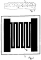
- FIG 2 the diagram is one on one in a plan Structured conductor track 2 applied to substrate 1 is shown.
- the trace is between pads for electrical Connection structured in the form of meanders.
- this trace z. B. is used as a heating element, cracks occur in the conductor track over time as a result of a material transport in the conductor track caused by the electrical current. Such cracks arise particularly where the conductor narrowing or mechanical damage, such as. B. scratches.
- Local thinning of the conductor track, ie constrictions in the current path and local mechanical stresses in the conductor track arise due to the roughness of the substrate surface being too large compared to the thickness of the conductor track.
- the widely used ceramic thin-film substrates on Al 2 O 3 have steps of up to 0.5 ⁇ m in height over a width of 0.1 ⁇ m on the top, which is too much for typical conductor tracks with a thickness of 1 ⁇ m to 2 ⁇ m.
- the conductor track is therefore applied to an extremely smooth substrate top.
- substrates are e.g. B. sapphire substrates with polished surfaces, flat quartz glass substrates, polished silicon wafers with an insulation layer, for. B. of SiO 2 , on the top or ceramic substrates, for. B. Al 2 O 3 , which have been smoothed by applying an additional layer (preferably also made of Al 2 O 3 or SiO 2 or Si 3 N 4 ).
- the additional layer can be applied by sputtering with a bias voltage on the substrate or with CVD (chemical vapor deposition). Conventional sputtering does not lead to success because it does not sufficiently smooth the top.
- CVD chemical vapor deposition
- Conventional sputtering does not lead to success because it does not sufficiently smooth the top.
- other high-temperature stable metal oxides such. B. MgO, Ga 2 O 3 or ZrO 2 can be used, which have a low conductivity compared to the conductor metal at high temperatures.
- Figure 1 is a top layer of the substrate through the Layer 30 shown in dashed lines. If this Layer is an oxide, can improve the adhesion of the Metal of the conductor tracks on the top of the substrate an extreme thin layer of an adhesion promoter. It is essential that the interface of the conductor track to The substrate is scratch-free and extremely smooth. Both usual dimensions of the conductor track of 1 to 2 microns thick and the roughness of the should be between 50 and 200 ⁇ m wide the conductor track provided top of the substrate no longer wear than 0.2 ⁇ m.
- the area of the track provided top of the substrate perpendicular to the middle level due to the areal extension of this Substrate top is formed, up and down at all Places deviates by no more than 0.1 ⁇ m from this middle level.
- An upper one to be observed in preferred versions Limit value for the roughness of the conductor track The top of the substrate is 0.04 ⁇ m.
- FIG. 3 shows a pattern applied to a substrate 1 in the diagram Track 2 shown that only curves with relative has a large radius of curvature. This prevents that at inner corners of the lateral conductor boundaries, where there are local maxima of current density, cracks occur. To limit the current density, therefore, only weak curvatures with large radii of curvature when structuring of conductor tracks approved.
- conventional trace structures as they e.g. B. for heating one High temperature gas sensors are used on the inside Corners have small radii of curvature, which because of the Production used photolithography about at least 2 microns be.
- all are Radius of curvature of the conductor track at least 30 microns, preferably at least 70 ⁇ m.
- the radius of curvature of the conductor track becomes each on the inner boundary line of the conductor track measured.
- the minimum radius of curvature should be there not be smaller than 70 ⁇ m. For space reasons it can however, especially with larger track widths, required be, in some places the radius of curvature to values to reduce down to 30 ⁇ m.
- a particularly suitable platinum alloy becomes. It is preferably an alloy of platinum and a platinum metal used, e.g. B. a platinum-rhodium alloy, a platinum-iridium alloy, a platinum-rhenium alloy, a platinum-palladium alloy or one Platinum-ruthenium alloy, with a platinum content of at least 50 percent by weight and at most 90 percent by weight, better of at least 65 percent by weight and at most 75 percent by weight.
- the conductor track made of a platinum-rhodium alloy with a Rhodium content of at least 10 percent by weight and at most 50 percent by weight. This conductor track metal has an increased Resistance to electromigration and at the same time one optimized resistance to oxygen.
- An optimal value the rhodium content of the alloy is between 25 Weight percent rhodium and a maximum of 35 weight percent rhodium at about 30 weight percent rhodium.
- Advantageous thicknesses of the conductor track are between 1 ⁇ m and 5 ⁇ m.
- the conductor track can additionally be covered with a passivation layer, which is preferably an oxide, e.g. B. is amorphous SiO 2 or Al 2 O 3 . No passivation is required for low intended operating temperatures.
- the conductor tracks can be produced by sputtering, electron beam evaporation or laser evaporation, whereby compact conductor track layers are obtained, or also with screen printing technology, whereby porous layers are obtained.
- the crystallite size is used to optimize the conductor stability in the metal of the conductor track in a certain size range held. Very stable conductor tracks result, if the crystallite sizes of the platinum alloy are in the range of 100 nm to 1000 nm, preferably in the vicinity of 500 nm in Range between 450 nm and 550 nm. Such crystallite sizes the conductor layer is obtained e.g. B. if the Conductor layer after the deposition of an annealing process of typically exposed to air for one hour at 1050 ° C becomes.
- the platinum-rhodium alloy preferably at a platinum-rhodium mixing ratio of 70 to 30 percent by weight is the conductor track compared to a conductor track hardened from pure platinum so that at one temperature of 950 ° C an increase in mechanical strength by about a factor of 6. That is sufficient for Suppression of the electromigration described at the beginning.
- an even higher hardening is not desirable because then adhesion problems of the conductor layer on the substrate material may occur.
- Rhodium is used because this alloy is the highest Resistant to oxygen.
- an electrically insulating or only weakly conductive material such as. B. an oxide (Al 2 O 3 ), a nitride (AlN), a silicon wafer covered with SiO 2 or Si 3 N 4 or a quartz glass.
- an adhesion promoter layer for example a metal oxide such as Ga 2 O 3 ) may be present between the substrate and the conductor track.
- Al 2 O 3 has particular advantages for passivating a conductor track serving as a heater structure for a gas sensor which is intended for the high-temperature range.
- Al 2 O 3 in contrast to other passivations, such as. B. La 2 O 3 , Y 2 O 3 , CeO 4 , TiO 2 or Fe 3 O 4 , the detection of chemically reducing gases is not disturbed.
- a preferred embodiment of the sensor according to the invention therefore includes gas-sensitive elements known per se, e.g. B.
- a layer of a semiconducting metal oxide, preferably Ga 2 O 3 with measuring electrodes that measure the electrical resistance of the metal oxide layer exposed to a gas, and a heater structure formed by a conductor track for heating the sensor to an intended temperature, at which a sufficient sensitivity compared to the gases to be detected, and passivation of this heater structure with a layer of Al 2 O 3 .
- the gas sensor is preferably set up in such a way that the temperature can be measured with the heater structure at the same time so that the temperature can be regulated to a constant value.
Landscapes
- General Physics & Mathematics (AREA)
- Physics & Mathematics (AREA)
- Chemical & Material Sciences (AREA)
- Immunology (AREA)
- Health & Medical Sciences (AREA)
- Life Sciences & Earth Sciences (AREA)
- Chemical Kinetics & Catalysis (AREA)
- General Health & Medical Sciences (AREA)
- Analytical Chemistry (AREA)
- Electrochemistry (AREA)
- Biochemistry (AREA)
- Pathology (AREA)
- Resistance Heating (AREA)
- Thermistors And Varistors (AREA)
- Measuring Temperature Or Quantity Of Heat (AREA)
Abstract
Description
- Figur 1
- zeigt den typischen Aufbau eine solchen Bauelementes im Querschnitt.
- Figur 2
- zeigt eine schematisierte Leiterbahnstruktur in Aufsicht.
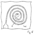
- Figuren 3, 4 und 5
- zeigen erfindungsgemäße Leiterbahnen in Aufsicht.
Claims (23)
- Bauelement mit einer planaren Leiterbahn (2) aus Metall, die auf einer Oberseite eines Substrates (1) aufgebracht und so strukturiert ist, daß sie durch Anlegen eines elektrischen Stromes als Heizung und/oder zur Bestimmung der Temperatur betrieben werden kann,bei dem die mit der Leiterbahn versehene Oberseite des Substrates in der Vertikalen um höchstens 0,1 µm beidseitig von einer mittleren Ebene abweicht.
- Bauelement nach Anspruch 1,bei dem die mit der Leiterbahn versehene Oberseite des Substrates in der Vertikalen um höchstens 0,02 µm beidseitig von einer mittleren Ebene abweicht.
- Bauelement nach Anspruch 1 oder 2,bei dem das Substrat ein Saphirsubstrat mit polierter Oberfläche ist.
- Bauelement nach Anspruch 1 oder 2,bei dem das Substrat ein planes Quarzglassubstrat ist.
- Bauelement nach Anspruch 1 oder 2,bei dem das Substrat Silizium mit einer Beschichtung aus SiO2 ist undbei dem die Leiterbahn auf dieser Beschichtung oder auf einer darauf aufgebrachten ebenen Passivierungsschicht oder Haftschicht (30) aufgebracht ist.
- Bauelement nach Anspruch 1 oder 2,bei dem das Substrat ein keramisches Material mit einer darauf aufgebrachten glättenden Beschichtung ist undbei dem die Leiterbahn auf dieser Beschichtung oder auf einer darauf aufgebrachten ebenen Passivierungsschicht oder Haftschicht (30) aufgebracht ist.
- Bauelement nach Anspruch 6,bei dem die Beschichtung SiO2 oder Si3N4 ist.
- Bauelement nach Anspruch 6,bei dem die Beschichtung ein hochtemperaturstabiles Metalloxid ist.
- Bauelement nach Anspruch 8,bei dem die Beschichtung aus einem Material aus der Gruppe von Al2O3, MgO, Ga2O3 und ZrO2 ist.
- Bauelement mit einer planaren Leiterbahn (2) aus Metall, die auf einem Substrat (1) aufgebracht und so strukturiert ist, daß sie durch Anlegen eines elektrischen Stromes als Heizung und/oder zur Bestimmung der Temperatur betrieben werden kann,bei dem der minimale Krümmungsradius der Leiterbahn 30 µm ist.
- Bauelement nach Anspruch 10,bei dem der minimale Krümmungsradius der Leiterbahn 70 µm ist.
- Bauelement nach Anspruch 10 oder 11,bei der die Leiterbahn als Spirale strukturiert ist.
- Bauelement nach Anspruch 12,bei der die Leiterbahn eine Fläche (10) für elektrischen Anschluß in der Mitte der Spirale besitzt.
- Bauelement nach einem der Ansprüche 1 bis 13,bei dem die Leiterbahn eine Dicke zwischen 0,5 µm und 10 µm besitzt.
- Bauelement mit einer planaren Leiterbahn (2) aus Metall, die auf einem Substrat (1) aufgebracht und so strukturiert ist, daß sie durch Anlegen eines elektrischen Stromes als Heizung und/oder zur Bestimmung der Temperatur betrieben werden kann,bei dem die Leiterbahn eine Platinlegierung ist.
- Bauelement nach Anspruch 15,bei dem die Leiterbahn eine Legierung aus der Gruppe von Platin-Rhodium-Legierung, Platin-Iridium-Legierung, Platin-Rhenium-Legierung, Platin-Ruthenium-Legierung und Platin-Palladium-Legierung ist.
- Bauelement nach Anspruch 16,bei dem die Leiterbahn eine Platin-Rhodium-Legierung ist mit einem Rhodiumanteil von mindestens 10 Gewichtsprozent und höchstens 50 Gewichtsprozent.
- Bauelement nach Anspruch 16,bei dem die Leiterbahn eine Platin-Rhodium-Legierung ist mit einem Rhodiumanteil von mindestens 25 Gewichtsprozent und höchstens 35 Gewichtsprozent.
- Bauelement nach Anspruch 16,bei dem die Leiterbahn eine Platinlegierung aus der Gruppe von Platin-Iridium-Legierung, Platin-Rhenium-Legierung, Platin-Ruthenium-Legierung und Platin-Palladium-Legierung mit einem Platinanteil von mindestens 50 Gewichtsprozent und höchstens 90 Gewichtsprozent ist.
- Bauelement nach Anspruch 16,bei dem die Leiterbahn eine Platinlegierung aus der Gruppe von Platin-Iridium-Legierung, Platin-Rhenium-Legierung, Platin-Ruthenium-Legierung und Platin-Palladium-Legierung mit einem Platinanteil von mindestens 65 Gewichtsprozent und höchstens 75 Gewichtsprozent ist.
- Bauelement nach einem der Ansprüche 15 bis 20,bei dem die Leiterbahn eine Dicke zwischen 1 µm und 5 µm besitzt.
- Bauelement nach einem der Ansprüche 15 bis 21,bei dem die Leiterbahn eine Kristallitgröße zwischen 100 nm und 1000 nm aufweist.
- Bauelement nach Anspruch 22,bei dem die Kristallitgröße zwischen 450 nm und 550 nm beträgt.
Applications Claiming Priority (2)
| Application Number | Priority Date | Filing Date | Title |
|---|---|---|---|
| DE19742696 | 1997-09-26 | ||
| DE1997142696 DE19742696A1 (de) | 1997-09-26 | 1997-09-26 | Bauelement mit planarer Leiterbahn |
Publications (2)
| Publication Number | Publication Date |
|---|---|
| EP0909950A2 true EP0909950A2 (de) | 1999-04-21 |
| EP0909950A3 EP0909950A3 (de) | 2000-11-08 |
Family
ID=7843822
Family Applications (1)
| Application Number | Title | Priority Date | Filing Date |
|---|---|---|---|
| EP98117990A Withdrawn EP0909950A3 (de) | 1997-09-26 | 1998-09-23 | Bauelement mit planarer Leiterbahn |
Country Status (2)
| Country | Link |
|---|---|
| EP (1) | EP0909950A3 (de) |
| DE (1) | DE19742696A1 (de) |
Cited By (3)
| Publication number | Priority date | Publication date | Assignee | Title |
|---|---|---|---|---|
| WO2009021734A1 (de) * | 2007-08-15 | 2009-02-19 | Heraeus Sensor Technology Gmbh | Russsensor mit glatter, reiner ai2o3-oberfläche |
| WO2010089024A3 (de) * | 2009-02-06 | 2010-11-25 | Heraeus Sensor Technology Gmbh | Widerstandsthermometer mit nichtleitfähigem zirconiumdioxid |
| US20220082455A1 (en) * | 2020-09-11 | 2022-03-17 | Hutchinson | Temperature sensor for a fluid circuit of motor vehicle |
Families Citing this family (11)
| Publication number | Priority date | Publication date | Assignee | Title |
|---|---|---|---|---|
| DE19936924C1 (de) * | 1999-08-05 | 2001-06-13 | Georg Bernitz | Vorrichtung zur Hochtemperaturerfassung und Verfahren zur Herstellung derselben |
| US6602428B2 (en) * | 2000-12-13 | 2003-08-05 | Denso Corporation | Method of manufacturing sensor having membrane structure |
| DE10103621C2 (de) * | 2001-01-27 | 2003-01-16 | Ego Elektro Geraetebau Gmbh | Passivierungspaste, Beschichtungsverfahren und Heizelement |
| DE102004060101B4 (de) * | 2004-06-03 | 2007-08-23 | Ust Umweltsensortechnik Gmbh | Anordnung zur Detektion von Luftinhaltsstoffen und Verfahren zum Betreiben der Anordnung |
| US7737700B2 (en) | 2005-11-23 | 2010-06-15 | Ust Umweltsensortechnik Gmbh | Arrangement and method for detecting air ingredients |
| DE102012110210B4 (de) | 2012-10-25 | 2017-06-01 | Heraeus Sensor Technology Gmbh | Hochtemperaturchip mit hoher Stabilität |
| DE102014104219B4 (de) * | 2014-03-26 | 2019-09-12 | Heraeus Nexensos Gmbh | Keramikträger sowie Sensorelement, Heizelement und Sensormodul jeweils mit einem Keramikträger und Verfahren zur Herstellung eines Keramikträgers |
| DE102014224687A1 (de) | 2014-12-03 | 2016-06-09 | Robert Bosch Gmbh | Metallschicht sowie Verfahren und Beschichtungsflüssigkeit für ihre Herstellung |
| DE102015216919A1 (de) | 2015-09-03 | 2017-03-09 | Robert Bosch Gmbh | Halbleiter-Bauelement |
| DE102015217298A1 (de) | 2015-09-10 | 2017-03-16 | Robert Bosch Gmbh | Halbleiter-Bauelement |
| DE202019002164U1 (de) | 2019-05-17 | 2019-06-21 | Heraeus Nexensos Gmbh | Verbesserter Hochtemperaturchip |
Family Cites Families (11)
| Publication number | Priority date | Publication date | Assignee | Title |
|---|---|---|---|---|
| US4139833A (en) * | 1976-11-22 | 1979-02-13 | Gould Inc. | Resistance temperature sensor |
| LU76937A1 (de) * | 1977-03-11 | 1978-10-18 | ||
| US4777351A (en) * | 1984-09-14 | 1988-10-11 | Raychem Corporation | Devices comprising conductive polymer compositions |
| JPS61188901A (ja) * | 1985-02-16 | 1986-08-22 | 株式会社日本自動車部品総合研究所 | 流量センサ用膜式抵抗 |
| GB2192459B (en) * | 1986-07-07 | 1990-12-19 | English Electric Valve Co Ltd | Hydrogen sulphide sensor |
| US4906968A (en) * | 1988-10-04 | 1990-03-06 | Cornell Research Foundation, Inc. | Percolating cermet thin film thermistor |
| DE4300084C2 (de) * | 1993-01-06 | 1995-07-27 | Heraeus Sensor Gmbh | Widerstandsthermometer mit einem Meßwiderstand |
| US5436457A (en) * | 1993-06-10 | 1995-07-25 | Horiba, Ltd. | Infrared gas analyzer |
| DE4428155C2 (de) * | 1994-08-09 | 1996-12-19 | Siemens Ag | Verfahren zur Herstellung eines Gassensors |
| JP3329644B2 (ja) * | 1995-07-21 | 2002-09-30 | 株式会社東芝 | 研磨パッド、研磨装置及び研磨方法 |
| DE19540194C1 (de) * | 1995-10-30 | 1997-02-20 | Heraeus Sensor Gmbh | Widerstandsthermometer aus einem Metall der Platingruppe |
-
1997
- 1997-09-26 DE DE1997142696 patent/DE19742696A1/de not_active Withdrawn
-
1998
- 1998-09-23 EP EP98117990A patent/EP0909950A3/de not_active Withdrawn
Non-Patent Citations (4)
| Title |
|---|
| BAKOGLU, H. B.: "Circuits, interconnections, and packaging for VLSI", 1990, ADDISON-WESLEY PUBLISHING COMPANY, INC. * |
| DR. PHIL. LOTHAR HAHN, CHEM.-ING. IRENE MUNKE U.A.: "Werkstoffkunde für die Elektrotechnik und Elektronik", 1986, VEB VERLAG TECHNIK, BERLIN * |
| DR. SC. TECHN. KLAUS SCHADE: "Halbleitertechnologie, Band 1, Mechanische und chemische Kristallbearbeitung, Schichtherstellung", 1981, VEB VERLAG TECHNIK, BERLIN * |
| SZE, S. M.: "Semiconductor Devices Physics and Technology", 1985, JOHN WILEY & SONS, NEW YORK * |
Cited By (5)
| Publication number | Priority date | Publication date | Assignee | Title |
|---|---|---|---|---|
| WO2009021734A1 (de) * | 2007-08-15 | 2009-02-19 | Heraeus Sensor Technology Gmbh | Russsensor mit glatter, reiner ai2o3-oberfläche |
| WO2010089024A3 (de) * | 2009-02-06 | 2010-11-25 | Heraeus Sensor Technology Gmbh | Widerstandsthermometer mit nichtleitfähigem zirconiumdioxid |
| US8730002B2 (en) | 2009-02-06 | 2014-05-20 | Heraeus Sensor Technology Gmbh | Non-conducting zirconium dioxide |
| US20220082455A1 (en) * | 2020-09-11 | 2022-03-17 | Hutchinson | Temperature sensor for a fluid circuit of motor vehicle |
| US11808640B2 (en) * | 2020-09-11 | 2023-11-07 | Hutchinson | Temperature sensor for a fluid circuit of motor vehicle |
Also Published As
| Publication number | Publication date |
|---|---|
| EP0909950A3 (de) | 2000-11-08 |
| DE19742696A1 (de) | 1999-05-06 |
Similar Documents
| Publication | Publication Date | Title |
|---|---|---|
| EP0909950A2 (de) | Bauelement mit planarer Leiterbahn | |
| DE3780560T2 (de) | Fuehler und verfahren zu dessen herstellung. | |
| DE69418615T2 (de) | Katalytischer gassensor | |
| EP0973020B1 (de) | Elektrischer Temperatur-Sensor mit Mehrfachschicht | |
| EP0723662B1 (de) | Sensor zum nachweis von stickoxid | |
| DE102007046900C5 (de) | Hochtemperatursensor und ein Verfahren zu dessen Herstellung | |
| EP1236038B1 (de) | Kapazitiver sensor | |
| EP1144968B1 (de) | Platintemperatursensor und herstellungsverfahren für denselben | |
| EP2606002B1 (de) | Mikromechanisches substrat für membran mit diffusionssperrschicht | |
| EP0571412A1 (de) | Hochtemperatur-platinmetall-temperatursensor | |
| DE2826515A1 (de) | Festkoerper-sensorelement | |
| DE112005000249B4 (de) | Dünnschichtgassensorkonfiguration | |
| DE102020122923A1 (de) | Sensorelement und Verfahren zur Herstellung eines Sensorelements | |
| DE4445359A1 (de) | Sensor zum Nachweis von brennbaren Gasen | |
| EP0199078B1 (de) | Integrierte Halbleiterschaltung mit einer aus Aluminium oder einer Aluminiumlegierung bestehenden Kontaktleiterbahnebene und einer als Diffusionsbarriere wirkenden Tantalsilizidzwischenschicht | |
| EP1601957B1 (de) | Ionensensitiver feldeffekttransistor und verfahren zum herstellen eines ionensensitiven feldeffekttransistors | |
| EP0024679B1 (de) | Selektiver Gassensor hoher Empfindlichkeit und Stabilität zum Nachweis und zur Messung des Verunreinigungsgehaltes von Luft auf der Basis von Metalloxidhalbleitern | |
| DE19918003A1 (de) | Elektrischer Temperatur-Sensor mit Mehrfachschicht | |
| EP0527259A1 (de) | Gassensor mit halbleitendem Galliumoxid | |
| DE3743398A1 (de) | Aufhaengung fuer eine sensoranordnung zum nachweis von gasen durch exotherme katalytische reaktionen | |
| WO2010130370A1 (de) | Fotolithographisch strukturierter dickschichtsensor | |
| DE19845112C2 (de) | Gassensor | |
| EP0905494A2 (de) | Hochtemperatursensor | |
| DE19805549C1 (de) | Verfahren zum Bond-Kontaktieren von elektronischen Bauelementchips, insbesondere Metalloxid-Gassensorchips | |
| DE4318327A1 (de) | Gassensor |
Legal Events
| Date | Code | Title | Description |
|---|---|---|---|
| PUAI | Public reference made under article 153(3) epc to a published international application that has entered the european phase |
Free format text: ORIGINAL CODE: 0009012 |
|
| AK | Designated contracting states |
Kind code of ref document: A2 Designated state(s): CH DE FR GB IT LI |
|
| AX | Request for extension of the european patent |
Free format text: AL;LT;LV;MK;RO;SI |
|
| RAP1 | Party data changed (applicant data changed or rights of an application transferred) |
Owner name: EPCOS AG |
|
| PUAL | Search report despatched |
Free format text: ORIGINAL CODE: 0009013 |
|
| AK | Designated contracting states |
Kind code of ref document: A3 Designated state(s): AT BE CH CY DE DK ES FI FR GB GR IE IT LI LU MC NL PT SE |
|
| AX | Request for extension of the european patent |
Free format text: AL;LT;LV;MK;RO;SI |
|
| 17P | Request for examination filed |
Effective date: 20010316 |
|
| AKX | Designation fees paid |
Free format text: CH DE FR GB IT LI |
|
| 17Q | First examination report despatched |
Effective date: 20011122 |
|
| STAA | Information on the status of an ep patent application or granted ep patent |
Free format text: STATUS: THE APPLICATION HAS BEEN WITHDRAWN |
|
| 18W | Application withdrawn |
Withdrawal date: 20020617 |