EP0909950A2 - Component with planar conductor pattern - Google Patents
Component with planar conductor pattern Download PDFInfo
- Publication number
- EP0909950A2 EP0909950A2 EP98117990A EP98117990A EP0909950A2 EP 0909950 A2 EP0909950 A2 EP 0909950A2 EP 98117990 A EP98117990 A EP 98117990A EP 98117990 A EP98117990 A EP 98117990A EP 0909950 A2 EP0909950 A2 EP 0909950A2
- Authority
- EP
- European Patent Office
- Prior art keywords
- platinum
- conductor track
- component according
- alloy
- substrate
- Prior art date
- Legal status (The legal status is an assumption and is not a legal conclusion. Google has not performed a legal analysis and makes no representation as to the accuracy of the status listed.)
- Withdrawn
Links
Images

Classifications
-
- G—PHYSICS
- G01—MEASURING; TESTING
- G01K—MEASURING TEMPERATURE; MEASURING QUANTITY OF HEAT; THERMALLY-SENSITIVE ELEMENTS NOT OTHERWISE PROVIDED FOR
- G01K7/00—Measuring temperature based on the use of electric or magnetic elements directly sensitive to heat ; Power supply therefor, e.g. using thermoelectric elements
- G01K7/16—Measuring temperature based on the use of electric or magnetic elements directly sensitive to heat ; Power supply therefor, e.g. using thermoelectric elements using resistive elements
- G01K7/18—Measuring temperature based on the use of electric or magnetic elements directly sensitive to heat ; Power supply therefor, e.g. using thermoelectric elements using resistive elements the element being a linear resistance, e.g. platinum resistance thermometer
-
- G—PHYSICS
- G01—MEASURING; TESTING
- G01N—INVESTIGATING OR ANALYSING MATERIALS BY DETERMINING THEIR CHEMICAL OR PHYSICAL PROPERTIES
- G01N27/00—Investigating or analysing materials by the use of electric, electrochemical, or magnetic means
- G01N27/02—Investigating or analysing materials by the use of electric, electrochemical, or magnetic means by investigating impedance
- G01N27/04—Investigating or analysing materials by the use of electric, electrochemical, or magnetic means by investigating impedance by investigating resistance
- G01N27/12—Investigating or analysing materials by the use of electric, electrochemical, or magnetic means by investigating impedance by investigating resistance of a solid body in dependence upon absorption of a fluid; of a solid body in dependence upon reaction with a fluid, for detecting components in the fluid
Definitions
- the present invention relates to a component with planar Conductor tracks, especially as a high temperature gas sensor or temperature sensor can be used.
- the traces have a structure of finger-shaped with each other can form interdigital electrodes with it the electrical conductivity of one on it semiconducting sensor layer can be measured and thus the chemical composition of a gas flowing over the sensor be determined.
- High temperature gas sensors in planar technology are by means of current-carrying heating structures heated to the required operating temperatures. To do this Usually used conductor tracks in thin or thick film technology applied to an upper side of the substrate are. The conductor tracks provided as heating can, for. B. be applied on the back of the substrate. Instead can also the conductor tracks acting as sensor electrodes even used as heaters. If the conductor tracks are made of a metal that is sufficiently high Has temperature coefficients of electrical conductivity, the resistance of the conductor track can also be used to determine the sensor temperature can be used. Regardless, you can in principle, structures of this type are also inexpensive Temperature sensors are used.
- Stable conductor tracks for higher temperatures can be produced by sintering the conductor track in ceramic.
- this solution is not suitable for high-temperature gas sensors based on Ga 2 O 3 , since the size of the sensor must be as small as possible to minimize the heating power required.
- This solution is also not suitable for high-temperature sensors, since the thermal mass of the sensor must also be as low as possible.
- the object of the present invention is to provide a component a planar metallic trace to indicate the operating temperature has a long service life around 1000 ° C.
- the component is intended in particular as a high-temperature gas sensor or can be implemented as a temperature sensor.
- the resistance the conductor track against long-term stress high temperature achieved in that the conductor track on a particularly flat, smooth surface is applied, that the conductor track is structured with large radii of curvature or that the conductor track made of a platinum alloy, preferably a platinum-rhodium alloy.
- a component is shown in cross section, at which has a planar conductor track 2 applied to a substrate 1 that is upward from a passivation layer 3 is sealed gas-tight.
- the passivation layer is intended to prevent that at the intended high operating temperatures the metal of the conductor tracks is removed and thereby the Traces become defective.
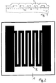
- FIG 2 the diagram is one on one in a plan Structured conductor track 2 applied to substrate 1 is shown.
- the trace is between pads for electrical Connection structured in the form of meanders.
- this trace z. B. is used as a heating element, cracks occur in the conductor track over time as a result of a material transport in the conductor track caused by the electrical current. Such cracks arise particularly where the conductor narrowing or mechanical damage, such as. B. scratches.
- Local thinning of the conductor track, ie constrictions in the current path and local mechanical stresses in the conductor track arise due to the roughness of the substrate surface being too large compared to the thickness of the conductor track.
- the widely used ceramic thin-film substrates on Al 2 O 3 have steps of up to 0.5 ⁇ m in height over a width of 0.1 ⁇ m on the top, which is too much for typical conductor tracks with a thickness of 1 ⁇ m to 2 ⁇ m.
- the conductor track is therefore applied to an extremely smooth substrate top.
- substrates are e.g. B. sapphire substrates with polished surfaces, flat quartz glass substrates, polished silicon wafers with an insulation layer, for. B. of SiO 2 , on the top or ceramic substrates, for. B. Al 2 O 3 , which have been smoothed by applying an additional layer (preferably also made of Al 2 O 3 or SiO 2 or Si 3 N 4 ).
- the additional layer can be applied by sputtering with a bias voltage on the substrate or with CVD (chemical vapor deposition). Conventional sputtering does not lead to success because it does not sufficiently smooth the top.
- CVD chemical vapor deposition
- Conventional sputtering does not lead to success because it does not sufficiently smooth the top.
- other high-temperature stable metal oxides such. B. MgO, Ga 2 O 3 or ZrO 2 can be used, which have a low conductivity compared to the conductor metal at high temperatures.
- Figure 1 is a top layer of the substrate through the Layer 30 shown in dashed lines. If this Layer is an oxide, can improve the adhesion of the Metal of the conductor tracks on the top of the substrate an extreme thin layer of an adhesion promoter. It is essential that the interface of the conductor track to The substrate is scratch-free and extremely smooth. Both usual dimensions of the conductor track of 1 to 2 microns thick and the roughness of the should be between 50 and 200 ⁇ m wide the conductor track provided top of the substrate no longer wear than 0.2 ⁇ m.
- the area of the track provided top of the substrate perpendicular to the middle level due to the areal extension of this Substrate top is formed, up and down at all Places deviates by no more than 0.1 ⁇ m from this middle level.
- An upper one to be observed in preferred versions Limit value for the roughness of the conductor track The top of the substrate is 0.04 ⁇ m.
- FIG. 3 shows a pattern applied to a substrate 1 in the diagram Track 2 shown that only curves with relative has a large radius of curvature. This prevents that at inner corners of the lateral conductor boundaries, where there are local maxima of current density, cracks occur. To limit the current density, therefore, only weak curvatures with large radii of curvature when structuring of conductor tracks approved.
- conventional trace structures as they e.g. B. for heating one High temperature gas sensors are used on the inside Corners have small radii of curvature, which because of the Production used photolithography about at least 2 microns be.
- all are Radius of curvature of the conductor track at least 30 microns, preferably at least 70 ⁇ m.
- the radius of curvature of the conductor track becomes each on the inner boundary line of the conductor track measured.
- the minimum radius of curvature should be there not be smaller than 70 ⁇ m. For space reasons it can however, especially with larger track widths, required be, in some places the radius of curvature to values to reduce down to 30 ⁇ m.
- a particularly suitable platinum alloy becomes. It is preferably an alloy of platinum and a platinum metal used, e.g. B. a platinum-rhodium alloy, a platinum-iridium alloy, a platinum-rhenium alloy, a platinum-palladium alloy or one Platinum-ruthenium alloy, with a platinum content of at least 50 percent by weight and at most 90 percent by weight, better of at least 65 percent by weight and at most 75 percent by weight.
- the conductor track made of a platinum-rhodium alloy with a Rhodium content of at least 10 percent by weight and at most 50 percent by weight. This conductor track metal has an increased Resistance to electromigration and at the same time one optimized resistance to oxygen.
- An optimal value the rhodium content of the alloy is between 25 Weight percent rhodium and a maximum of 35 weight percent rhodium at about 30 weight percent rhodium.
- Advantageous thicknesses of the conductor track are between 1 ⁇ m and 5 ⁇ m.
- the conductor track can additionally be covered with a passivation layer, which is preferably an oxide, e.g. B. is amorphous SiO 2 or Al 2 O 3 . No passivation is required for low intended operating temperatures.
- the conductor tracks can be produced by sputtering, electron beam evaporation or laser evaporation, whereby compact conductor track layers are obtained, or also with screen printing technology, whereby porous layers are obtained.
- the crystallite size is used to optimize the conductor stability in the metal of the conductor track in a certain size range held. Very stable conductor tracks result, if the crystallite sizes of the platinum alloy are in the range of 100 nm to 1000 nm, preferably in the vicinity of 500 nm in Range between 450 nm and 550 nm. Such crystallite sizes the conductor layer is obtained e.g. B. if the Conductor layer after the deposition of an annealing process of typically exposed to air for one hour at 1050 ° C becomes.
- the platinum-rhodium alloy preferably at a platinum-rhodium mixing ratio of 70 to 30 percent by weight is the conductor track compared to a conductor track hardened from pure platinum so that at one temperature of 950 ° C an increase in mechanical strength by about a factor of 6. That is sufficient for Suppression of the electromigration described at the beginning.
- an even higher hardening is not desirable because then adhesion problems of the conductor layer on the substrate material may occur.
- Rhodium is used because this alloy is the highest Resistant to oxygen.
- an electrically insulating or only weakly conductive material such as. B. an oxide (Al 2 O 3 ), a nitride (AlN), a silicon wafer covered with SiO 2 or Si 3 N 4 or a quartz glass.
- an adhesion promoter layer for example a metal oxide such as Ga 2 O 3 ) may be present between the substrate and the conductor track.
- Al 2 O 3 has particular advantages for passivating a conductor track serving as a heater structure for a gas sensor which is intended for the high-temperature range.
- Al 2 O 3 in contrast to other passivations, such as. B. La 2 O 3 , Y 2 O 3 , CeO 4 , TiO 2 or Fe 3 O 4 , the detection of chemically reducing gases is not disturbed.
- a preferred embodiment of the sensor according to the invention therefore includes gas-sensitive elements known per se, e.g. B.
- a layer of a semiconducting metal oxide, preferably Ga 2 O 3 with measuring electrodes that measure the electrical resistance of the metal oxide layer exposed to a gas, and a heater structure formed by a conductor track for heating the sensor to an intended temperature, at which a sufficient sensitivity compared to the gases to be detected, and passivation of this heater structure with a layer of Al 2 O 3 .
- the gas sensor is preferably set up in such a way that the temperature can be measured with the heater structure at the same time so that the temperature can be regulated to a constant value.
Landscapes
- Physics & Mathematics (AREA)
- General Physics & Mathematics (AREA)
- Chemical & Material Sciences (AREA)
- Chemical Kinetics & Catalysis (AREA)
- Electrochemistry (AREA)
- Health & Medical Sciences (AREA)
- Life Sciences & Earth Sciences (AREA)
- Analytical Chemistry (AREA)
- Biochemistry (AREA)
- General Health & Medical Sciences (AREA)
- Immunology (AREA)
- Pathology (AREA)
- Resistance Heating (AREA)
- Thermistors And Varistors (AREA)
- Measuring Temperature Or Quantity Of Heat (AREA)
Abstract
Description
Die vorliegende Erfindung betrifft ein Bauelement mit planaren Leiterbahnen, das insbesondere als Hochtemperaturgassensor oder Temperaturfühler verwendet werden kann.The present invention relates to a component with planar Conductor tracks, especially as a high temperature gas sensor or temperature sensor can be used.
Sensoren mit einer planaren Leiterbahnstruktur auf einer Substratoberseite werden z. B. als Gassensoren verwendet. Planare metallische Leiterbahnen auf einem Substrat, die gegen hohe Temperaturen im Bereich um 1000°C resistent sind, werden auch zur Realisierung von Infrarot-Lichtquellen oder zur Auslösung chemischer Reaktionen verwendet. Außerdem können damit besonders stabile planare Temperatursensoren hergestellt werden.Sensors with a planar conductor structure on one Substrate top z. B. used as gas sensors. Planar metallic conductor tracks on a substrate that oppose high temperatures around 1000 ° C are resistant, are also used to realize infrared light sources or used to trigger chemical reactions. You can also This produces particularly stable planar temperature sensors become.
Wenn die Leiterbahnen eine Struktur von fingerförmig miteinander verzahnten Interdigitalelektroden bilden, kann damit die elektrische Leitfähigkeit einer sich darauf befindenden halbleitenden Sensorschicht gemessen werden und damit die chemische Zusammensetzung eines den Sensor überströmenden Gases festgestellt werden. Hochtemperaturgassensoren in Planartechnologie werden mittels stromdurchflossener Heizstrukturen auf die benötigten Betriebstemperaturen beheizt. Dazu werden üblicherweise Leiterbahnen verwendet, die in Dünn- oder Dickschichttechnik auf eine Oberseite des Substrates aufgebracht sind. Die als Heizung vorgesehenen Leiterbahnen können z. B. auf der Rückseite des Substrates aufgebracht sein. Statt dessen können auch die als Sensorelektroden fungierenden Leiterbahnen selbst als Heizungen verwendet werden. Falls die Leiterbahnen aus einem Metall sind, das einen ausreichend hohen Temperaturkoeffizienten der elektrischen Leitfähigkeit besitzt, kann der Widerstand der Leiterbahn auch zur Bestimmung der Sensortemperatur verwendet werden. Unabhängig davon können derartige Strukturen prinzipiell auch als kostengünstige Temperaturfühler eingesetzt werden. If the traces have a structure of finger-shaped with each other can form interdigital electrodes with it the electrical conductivity of one on it semiconducting sensor layer can be measured and thus the chemical composition of a gas flowing over the sensor be determined. High temperature gas sensors in planar technology are by means of current-carrying heating structures heated to the required operating temperatures. To do this Usually used conductor tracks in thin or thick film technology applied to an upper side of the substrate are. The conductor tracks provided as heating can, for. B. be applied on the back of the substrate. Instead can also the conductor tracks acting as sensor electrodes even used as heaters. If the conductor tracks are made of a metal that is sufficiently high Has temperature coefficients of electrical conductivity, the resistance of the conductor track can also be used to determine the sensor temperature can be used. Regardless, you can in principle, structures of this type are also inexpensive Temperature sensors are used.
Bei Temperaturen oberhalb von 600°C sind selbst Leiterbahnen aus hochschmelzenden Edelmetallen wie Gold oder Platin nicht mehr stabil. Im allgemeinen kommt es durch Diffusionsprozesse oder durch Gasphasentransport (z. B. durch Bildung flüchtiger Platinoxide bei Platinleiterbahnen, die dem Luftsauerstoff ausgesetzt werden) zu einem Materialverlust der Leiterbahn. Dadurch ergibt sich eine Verengung des Querschnittes der Leiterbahnen, die eine Änderung des elektrischen Widerstands der Leiterbahnstruktur bewirkt. Wird der elektrische Widerstand zur Bestimmung der Temperatur benutzt, so ist die gemessene Temperatur systematisch zu hoch. Wird die Heizung mit konstanter elektrischer Spannung betrieben, tritt außerdem eine Verminderung der Heizleistung auf. Bei fortschreitender Alterung der Leiterbahnen durch Materialverlust kommt es schließlich zu einer Unterbrechung der Leiterbahn, so daß die Heizung ganz ausfällt.At temperatures above 600 ° C there are even conductor tracks not from high-melting precious metals such as gold or platinum more stable. Generally it comes through diffusion processes or by gas phase transport (e.g. by formation of volatile Platinum oxides in platinum conductor tracks that release atmospheric oxygen exposed) to a loss of material in the conductor track. This results in a narrowing of the cross section of the conductor tracks, which is a change in the electrical resistance of the Conductor structure causes. Will the electrical resistance used to determine the temperature is the measured Systematic temperature too high. Is the heating constant? operated electrical voltage, also occurs Reduction in heating output. As aging progresses of the conductor tracks due to material loss eventually occurs to an open circuit so that the heater fails completely.
Durch Passivierungen, die die Leiterbahnstruktur gasdicht bedecken, wird versucht, den Materialverlust zu unterbinden. Bei kommerziellen Anbietern von Dünnschicht-Temperaturfühlern werden die Leiterbahnen mit hochschmelzenden Gläsern abgedeckt. Bei derartigen Sensoren liegt die obere Grenze der Betriebstemperatur allerdings bei etwa 600 bis 700°C. Diese Temperaturbegrenzung rührt daher, daß selbst hochschmelzende Gläser in diesem Temperaturbereich weich werden, zu kristallisieren beginnen und damit ihre Gasdichtigkeit verlieren.Through passivations that cover the conductor track structure in a gas-tight manner, an attempt is made to prevent the loss of material. At commercial suppliers of thin-film temperature sensors the conductor tracks are covered with high-melting glasses. With such sensors, the upper limit of the operating temperature is however at about 600 to 700 ° C. This Temperature limitation stems from the fact that even high-melting Glasses in this temperature range become soft, crystallize start and lose their gas tightness.
Stabile Leiterbahnen für höhere Temperaturen können dadurch hergestellt werden, daß die Leiterbahn in Keramik eingesintert wird. Diese Lösung ist jedoch für Hochtemperaturgassensoren auf Ga2O3-Basis nicht geeignet, da die Größe des Sensors zur Minimierung der erforderlichen Heizleistung möglichst gering sein muß. Auch für Hochtemperatur-Meßfühler bietet sich diese Lösung nicht an, da auch hier die thermische Masse des Fühlers möglichst gering sein muß. Stable conductor tracks for higher temperatures can be produced by sintering the conductor track in ceramic. However, this solution is not suitable for high-temperature gas sensors based on Ga 2 O 3 , since the size of the sensor must be as small as possible to minimize the heating power required. This solution is also not suitable for high-temperature sensors, since the thermal mass of the sensor must also be as low as possible.
Bei Langzeitbetrieb dieser Sensoren bei Temperaturen um 950°C kommt es zu Schädigungen der Leiterbahnstruktur trotz intakter Passivierungsschicht. Diese sind strombedingt, resultieren also nicht allein aus den hohen Temperaturen, und sind auf den Mechanismus der Elektromigration zurückzuführen. Wegen der hohen Stromdichte in den als Heizung verwendeten Leiterbahnen von typisch 105 A/cm2 und infolge einer Erweichung des Leiterbahnmetalls bei den hohen vorherrschenden Temperaturen kommt es zu einem strombedingten Materialtransport von Atomen des Leiterbahnmetalls entlang von Korngrenzen in Stromrichtung. Dieser Materialtransport bewirkt mechanische Spannungen im Leiterbahnmaterial und führt im ungünstigen Fall zu lokaler Rißbildung. Das führt wiederum zu einer Änderung der Strompfade und erneuter Rißbildung, so daß bei Überschreiten einer gewissen kritischen Schwelle die Temperatur und die Stromdichte bis zu einem Ausfall der Sensorheizung führen können.Long-term operation of these sensors at temperatures around 950 ° C leads to damage to the conductor track structure despite the intact passivation layer. These are electricity-related, so they do not result solely from the high temperatures, and are due to the mechanism of electromigration. Because of the high current density of typically 10 5 A / cm 2 in the conductor tracks used for heating and due to a softening of the conductor track metal at the high prevailing temperatures, there is a current-related material transport of atoms of the conductor track metal along grain boundaries in the current direction. This material transport causes mechanical stresses in the conductor track material and, in the worst case, leads to local crack formation. This in turn leads to a change in the current paths and renewed crack formation, so that if a certain critical threshold is exceeded, the temperature and the current density can lead to a failure of the sensor heating.
Aufgabe der vorliegenden Erfindung ist es, ein Bauelement mit einer planaren metallischen Leiterbahn anzugeben, die bei Betriebstemperaturen um 1000°C eine hohe Lebensdauer aufweist. Das Bauelement soll insbesondere als Hochtemperatur-Gassensor oder als Temperaturfühler realisierbar sein.The object of the present invention is to provide a component a planar metallic trace to indicate the operating temperature has a long service life around 1000 ° C. The component is intended in particular as a high-temperature gas sensor or can be implemented as a temperature sensor.
Diese Aufgabe wird mit dem Bauelement mit den Merkmalen des
Anspruches 1, des Anspruches 10 bzw. des Anspruches 15 gelöst.
Ausgestaltungen ergeben sich aus den abhängigen Ansprüchen.This task is performed with the component with the characteristics of
Bei dem erfindungsgemäßen Bauelement wird die Widerstandsfähigkeit der Leiterbahn gegen langzeitige Beanspruchung bei hoher Temperatur dadurch erreicht, daß die Leiterbahn auf einer besonders ebenen, glatten Oberfläche aufgebracht wird, daß die Leiterbahn mit großen Krümmungsradien strukturiert wird oder daß die Leiterbahn aus einer Platinlegierung, vorzugsweise einer Platin-Rhodium-Legierung, hergestellt wird. In the component according to the invention, the resistance the conductor track against long-term stress high temperature achieved in that the conductor track on a particularly flat, smooth surface is applied, that the conductor track is structured with large radii of curvature or that the conductor track made of a platinum alloy, preferably a platinum-rhodium alloy.
Es können auch zwei oder alle dieser Mittel gleichzeitig eingesetzt werden.Two or all of these agents can also be used simultaneously become.
Es folgt eine genauere Beschreibung des erfindungsgemäßen Bauelementes anhand der Figuren 1 bis 5.
Figur 1- zeigt den typischen Aufbau eine solchen Bauelementes im Querschnitt.
Figur 2- zeigt eine schematisierte Leiterbahnstruktur in Aufsicht.
Figuren 3, 4 und 5- zeigen erfindungsgemäße Leiterbahnen in Aufsicht.
- Figure 1
- shows the typical structure of such a component in cross section.
- Figure 2
- shows a schematic conductor track structure in supervision.
- Figures 3, 4 and 5
- show conductor tracks according to the invention in supervision.
In Figur 1 ist ein Bauelement im Querschnitt dargestellt, bei
dem auf einem Substrat 1 eine planare Leiterbahn 2 aufgebracht
ist, die nach oben von einer Passivierungsschicht 3
gasdicht verschlossen ist. Die Passivierungsschicht soll verhindern,
daß bei den vorgesehenen hohen Betriebstemperaturen
das Metall der Leiterbahnen abgetragen wird und dadurch die
Leiterbahnen schadhaft werden.In Figure 1, a component is shown in cross section, at
which has a
In Figur 2 ist im Schema in einer Aufsicht eine auf einem
Substrat 1 aufgebrachte strukturierte Leiterbahn 2 dargestellt.
Die Leiterbahn ist zwischen Anschlußflächen für elektrischen
Anschluß in Form von Mäandern strukturiert.In Figure 2, the diagram is one on one in a plan
Wenn diese Leiterbahn z. B. als Heizelement verwendet wird, treten als Folge eines durch den elektrischen Strom bedingten Materialtransportes in der Leiterbahn an kritischen Stellen im Laufe der Zeit Risse in der Leiterbahn auf. Derartige Risse entstehen besonders dort, wo die Leiterbahn Verengungen oder mechanische Beschädigungen, wie z. B. Kratzer, aufweist. Lokale Verdünnungen der Leiterbahn, d. h. Einschnürungen des Strompfades und lokale mechanische Spannungen in der Leiterbahn entstehen aufgrund von im Vergleich zur Dicke der Leiterbahn zu großer Rauhigkeit der Substratoberfläche. Die vielfach verwendeten keramischen Dünnschichtsubstrate auf Al2O3 weisen Stufen von bis zu 0,5 µm Höhe über eine Breite von 0,1 µm an der Oberseite auf, was für typische Leiterbahnen mit einer Dicke von 1 µm bis 2 µm zuviel ist. Bei einer Ausgestaltung des erfindungsgemäßen Bauelementes ist die Leiterbahn daher auf einer extrem glatten Substratoberseite aufgebracht. Solche Substrate sind z. B. Saphirsubstrate mit polierten Oberflächen, plane Quarzglassubstrate, polierte Siliziumwafer mit einer Isolationsschicht, z. B. aus SiO2, an der Oberseite oder keramische Substrate, z. B. Al2O3, die durch Aufbringen einer zusätzlichen Schicht (vorzugsweise auch aus Al2O3 oder aus SiO2 oder Si3N4) geglättet worden sind. Das Aufbringen der zusätzlichen Schicht kann durch Sputterverfahren mit einer Bias-Spannung am Substrat oder mit CVD-Verfahren (chemical vapour deposition) erfolgen. Konventionelles Sputterverfahren führt nicht zum Erfolg, da damit keine ausreichende Glättung der Oberseite erzielt wird. Zum Glätten der Substratoberseite können auch andere hochtemperaturstabile Metalloxide wie z. B. MgO, Ga2O3 oder ZrO2 verwendet werden, die bei hohen Temperaturen eine im Vergleich zum Leiterbahnmetall geringe Leitfähigkeit aufweisen.If this trace z. B. is used as a heating element, cracks occur in the conductor track over time as a result of a material transport in the conductor track caused by the electrical current. Such cracks arise particularly where the conductor narrowing or mechanical damage, such as. B. scratches. Local thinning of the conductor track, ie constrictions in the current path and local mechanical stresses in the conductor track arise due to the roughness of the substrate surface being too large compared to the thickness of the conductor track. The widely used ceramic thin-film substrates on Al 2 O 3 have steps of up to 0.5 µm in height over a width of 0.1 µm on the top, which is too much for typical conductor tracks with a thickness of 1 µm to 2 µm. In one configuration of the component according to the invention, the conductor track is therefore applied to an extremely smooth substrate top. Such substrates are e.g. B. sapphire substrates with polished surfaces, flat quartz glass substrates, polished silicon wafers with an insulation layer, for. B. of SiO 2 , on the top or ceramic substrates, for. B. Al 2 O 3 , which have been smoothed by applying an additional layer (preferably also made of Al 2 O 3 or SiO 2 or Si 3 N 4 ). The additional layer can be applied by sputtering with a bias voltage on the substrate or with CVD (chemical vapor deposition). Conventional sputtering does not lead to success because it does not sufficiently smooth the top. To smooth the top of the substrate, other high-temperature stable metal oxides such. B. MgO, Ga 2 O 3 or ZrO 2 can be used, which have a low conductivity compared to the conductor metal at high temperatures.
In Figur 1 ist eine oberste Schicht des Substrates durch die
gestrichelt eingezeichnete Schicht 30 angedeutet. Falls diese
Schicht ein Oxid ist, kann zur Verbesserung der Haftung des
Metalles der Leiterbahnen auf der Substratoberseite eine extrem
dünne Schicht aus einem Haftvermittler vorhanden sein.
Wesentlich ist dabei, daß die Grenzfläche der Leiterbahn zum
Substrat hin frei von Kratzern und extrem glatt ist. Bei den
üblichen Abmessungen der Leiterbahn von 1 bis 2 µm Dicke und
zwischen 50 und 200 µm Breite sollte die Rauigkeit der mit
der Leiterbahn versehenen Oberseite des Substrates nicht mehr
als 0,2 µm tragen. D. h., daß die Fläche der mit der Leiterbahn
versehenen Oberseite des Substrates senkrecht zu der
mittleren Ebene, die durch die flächige Ausdehnung dieser
Substratoberseite gebildet wird, nach oben und unten an allen
Stellen um höchstens 0,1 µm von dieser mittleren Ebene abweicht.
Ein bei bevorzugten Ausführungen einzuhaltender oberer
Grenzwert für die Rauigkeit der mit der Leiterbahn versehenen
Oberseite des Substrates liegt bei 0,04 µm.In Figure 1 is a top layer of the substrate through the
In Figur 3 ist im Schema eine auf einem Substrat 1 aufgebrachte
Leiterbahn 2 dargestellt, die nur Rundungen mit relativ
großem Krümmungsradius aufweist. Damit wird verhindert,
daß an inneren Ecken der seitlichen Leiterbahnbegrenzungen,
an denen lokale Maxima der Stromdichte vorherrschen, Risse
auftreten. Um die Stromdichte zu begrenzen, werden daher nur
schwache Krümmungen mit großen Krümmungsradien bei der Strukturierung
der Leiterbahnen zugelassen. Bei herkömmlichen Leiterbahnstrukturen,
wie sie z. B. für die Heizung eines
Hochtemperatur-Gassensors eingesetzt werden, sind an inneren
Ecken kleine Krümmungsradien vorhanden, die wegen der bei der
Herstellung verwendeten Photolithographie ca. mindestens 2 µm
betragen. Bei dem erfindungsgemäßen Bauelement betragen alle
Krümmungsradien der Leiterbahn mindestens 30 µm, vorzugsweise
mindestens 70 µm. Der Krümmungsradius der Leiterbahn wird dabei
jeweils an der inneren Begrenzungslinie der Leiterbahn
gemessen. Der minimale dort auftretende Krümmungsradius sollte
nicht kleiner als 70 µm sein. Aus Platzgründen kann es
aber, insbesondere bei größeren Leiterbahnbreiten, erforderlich
sein, an manchen Stellen den Krümmungsradius auf Werte
bis herab zu 30 µm zu reduzieren.FIG. 3 shows a pattern applied to a
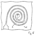
Wird die Leiterbahn entsprechend der Aufsicht, die in Figur 4 dargestellt ist, als Spirale strukturiert, ist der Krümmungsradius längs der Leiterbahn mit Ausnahme des Wendepunktes ganz im Inneren überall sehr groß. Die in der Figur 4 eingetragenen typischen Abmessungen sind nur als Beispiele zu verstehen und können im Einzelfall beliebig abgewandelt sein.If the conductor track is in accordance with the supervision shown in FIG is structured as a spiral, is the radius of curvature along the conductor track with the exception of the turning point very big everywhere inside. The entered in Figure 4 typical dimensions are only to be understood as examples and can be modified as required in individual cases.
Eine weitere Möglichkeit, den Krümmungsradius zusätzlich zu
vergrößern, ergibt sich durch Verwendung einer Spirale mit
einer Anschlußfläche für elektrische Kontaktierung in der
Mitte, wie sie in Figur 5 dargestellt ist. Die auf dem
Substrat 1 aufgebrachte Leiterbahn 2 besitzt in der Mitte eine
verbreiterte Anschlußfläche 10, die für den elektrischen
Anschluß vorgesehen ist. Die Leiterbahn ist dann spiralig nur
nach innen geführt und braucht nicht in entgegengesetztem Umlaufsinn
wieder zu einer Anschlußfläche am Rand des Bauelementes
herausgeführt zu werden. Eine kritische Stelle der
Leiterbahn im Innern der Spirale, an der der Krümmungsradius
zwangsläufig niedriger sein muß, entfällt bei dieser Anordnung
gemäß Figur 5. Bei Leiterbahnen einer Dicke zwischen
0,5 µm und 10 µm kann mit einer Vergrößerung des minimalen
Krümmungsradius eine wesentliche Verbesserung der Dauerhaftigkeit
erzielt werden.Another way to add the radius of curvature
enlarge, results from using a spiral with
a pad for electrical contacting in the
Middle, as shown in Figure 5. The one on the
Eine Verbesserung ergibt sich auch dadurch, daß für derartige Leiterbahnen eine besonders geeignete Platinlegierung verwendet wird. Es wird vorzugsweise eine Legierung aus Platin und einem Platinmetall verwendet, z. B. eine Platin-Rhodium-Legierung, eine Platin-Iridium-Legierung, eine Platin-Rhenium-Legierung, eine Platin-Palladium-Legierung oder eine Platin-Ruthenium-Legierung, mit einem Platinanteil von mindestens 50 Gewichtsprozent und höchstens 90 Gewichtsprozent, besser von mindestens 65 Gewichtsprozent und höchstens 75 Gewichtsprozent. Bei einer bevorzugten Ausführungsform besteht die Leiterbahn aus einer Platin-Rhodium-Legierung mit einem Rhodiumanteil von mindestens 10 Gewichtsprozent und höchstens 50 Gewichtsprozent. Dieses Leiterbahnmetall weist eine erhöhte Beständigkeit gegenüber Elektromigration und zugleich eine optimierte Beständigkeit gegenüber Sauerstoff auf. Ein Optimalwert für den Rhodiumanteil der Legierung liegt zwischen 25 Gewichtsprozent Rhodium und höchstens 35 Gewichtsprozent Rhodium bei etwa 30 Gewichtsprozent Rhodium.An improvement also results from the fact that for such Conductors used a particularly suitable platinum alloy becomes. It is preferably an alloy of platinum and a platinum metal used, e.g. B. a platinum-rhodium alloy, a platinum-iridium alloy, a platinum-rhenium alloy, a platinum-palladium alloy or one Platinum-ruthenium alloy, with a platinum content of at least 50 percent by weight and at most 90 percent by weight, better of at least 65 percent by weight and at most 75 percent by weight. In a preferred embodiment the conductor track made of a platinum-rhodium alloy with a Rhodium content of at least 10 percent by weight and at most 50 percent by weight. This conductor track metal has an increased Resistance to electromigration and at the same time one optimized resistance to oxygen. An optimal value the rhodium content of the alloy is between 25 Weight percent rhodium and a maximum of 35 weight percent rhodium at about 30 weight percent rhodium.
Vorteilhafte Dicken der Leiterbahn liegen zwischen 1 µm und 5 µm. Die Leiterbahn kann zusätzlich mit einer Passivierungsschicht abgedeckt sein, die vorzugsweise ein Oxid, z. B. amorphes SiO2 oder Al2O3 ist. Für geringe vorgesehene Betriebtemperaturen ist keine Passivierung notwendig. Die Leiterbahnen können durch Sputtern, Elektronenstrahlverdampfen oder Laserverdampfen hergestellt werden, womit kompakte Leiterbahnschichten erhalten werden, oder auch mit Siebdrucktechnik, wobei poröse Schichten erhalten werden.Advantageous thicknesses of the conductor track are between 1 µm and 5 µm. The conductor track can additionally be covered with a passivation layer, which is preferably an oxide, e.g. B. is amorphous SiO 2 or Al 2 O 3 . No passivation is required for low intended operating temperatures. The conductor tracks can be produced by sputtering, electron beam evaporation or laser evaporation, whereby compact conductor track layers are obtained, or also with screen printing technology, whereby porous layers are obtained.
Zur Optimierung der Leiterbahnstabilität wird die Kristallitgröße in dem Metall der Leiterbahn in einer bestimmten Größenspanne gehalten. Sehr stabile Leiterbahnen ergeben sich, falls die Kristallitgrößen der Platinlegierung im Bereich von 100 nm bis 1000 nm, vorzugsweise in der Nähe von 500 nm im Bereich zwischen 450 nm und 550 nm liegen. Derartige Kristallitgrößen der Leiterbahnschicht erhält man z. B., wenn die Leiterbahnschicht nach der Abscheidung einem Temperprozeß von typischerweise einer Stunde bei 1050°C an Luft ausgesetzt wird. Durch die Verwendung der Platin-Rhodium-Legierung, vorzugsweise bei einem Platin-Rhodium-Mischverhältnis von 70 zu 30 Gewichtsprozenten, ist die Leiterbahn gegenüber einer Leiterbahn aus reinem Platin derart gehärtet, daß bei einer Temperatur von 950°C eine Erhöhung der mechanischen Festigkeit um etwa den Faktor 6 erreicht wird. Das ist ausreichend zur Unterdrückung der eingangs beschriebenen Elektromigration. Eine noch höhere Härtung ist dagegen nicht wünschenswert, da dann Haftungsprobleme der Leiterbahnschicht auf dem Substratmaterial auftreten können. Zum Legieren des Platin wird vorzugsweise Rhodium verwendet, da diese Legierung die höchste Beständigkeit gegenüber Sauerstoff aufweist. Bei dem Mischungsverhältnis von 70 zu 30 Gewichtsprozenten kommt der Materialabtrag aufgrund der Bildung der flüchtigen Oxide nahezu vollständig zum Erliegen.The crystallite size is used to optimize the conductor stability in the metal of the conductor track in a certain size range held. Very stable conductor tracks result, if the crystallite sizes of the platinum alloy are in the range of 100 nm to 1000 nm, preferably in the vicinity of 500 nm in Range between 450 nm and 550 nm. Such crystallite sizes the conductor layer is obtained e.g. B. if the Conductor layer after the deposition of an annealing process of typically exposed to air for one hour at 1050 ° C becomes. By using the platinum-rhodium alloy, preferably at a platinum-rhodium mixing ratio of 70 to 30 percent by weight is the conductor track compared to a conductor track hardened from pure platinum so that at one temperature of 950 ° C an increase in mechanical strength by about a factor of 6. That is sufficient for Suppression of the electromigration described at the beginning. However, an even higher hardening is not desirable because then adhesion problems of the conductor layer on the substrate material may occur. For alloying the platinum is preferred Rhodium is used because this alloy is the highest Resistant to oxygen. With the mixing ratio from 70 to 30 percent by weight Material removal almost due to the formation of volatile oxides completely to a halt.
Für das Substrat kommt ein elektrisch isolierendes oder nur schwach leitendes Material in Frage, wie z. B. ein Oxid (Al2O3), ein Nitrid (AlN), ein mit SiO2 oder Si3N4 bedeckter Siliziumwafer oder ein Quarzglas. Zwischen dem Substrat und der Leiterbahn kann ggf. auch bei dieser Ausführungsform eine Haftvermittlerschicht (z. B. ein Metalloxid wie z. B. Ga2O3) vorhanden sein. For the substrate, an electrically insulating or only weakly conductive material, such as. B. an oxide (Al 2 O 3 ), a nitride (AlN), a silicon wafer covered with SiO 2 or Si 3 N 4 or a quartz glass. In this embodiment, too, an adhesion promoter layer (for example a metal oxide such as Ga 2 O 3 ) may be present between the substrate and the conductor track.
Es wurde erkannt, daß Al2O3 besondere Vorteile zur Passivierung einer als Heizerstruktur für einen Gassensor, der für den Hochtemperaturbereich vorgesehen ist, dienenden Leiterbahn aufweist. Durch Al2O3 wird im Gegensatz zu anderen Passivierungen, wie z. B. La2O3, Y2O3, CeO4, TiO2 oder Fe3O4, die Detektion chemisch reduzierender Gase nicht gestört. Eine bevorzugte Ausführungsform des erfindungsgemäßen Sensors umfaßt daher an sich bekannte gassensitive Elemente, z. B. eine Schicht aus einem halbleitenden Metalloxid, vorzugsweise Ga2O3, mit Meßelektroden, die den elektrischen Widerstand der einem Gas ausgesetzten Metalloxidschicht messen, und eine durch eine Leiterbahn gebildete Heizerstruktur zum Aufheizen des Sensors auf eine vorgesehene Temperatur, bei der eine ausreichende Sensitivität gegenüber den zu detektierenden Gasen erreicht ist, sowie eine Passivierung dieser Heizerstruktur mit einer Schicht aus Al2O3. Vorzugsweise ist der Gassensor so eingerichtet, daß mit der Heizerstruktur zugleich die Temperatur gemessen werden kann, damit die Temperatur auf einen konstanten Wert geregelt werden kann.It was recognized that Al 2 O 3 has particular advantages for passivating a conductor track serving as a heater structure for a gas sensor which is intended for the high-temperature range. Al 2 O 3 , in contrast to other passivations, such as. B. La 2 O 3 , Y 2 O 3 , CeO 4 , TiO 2 or Fe 3 O 4 , the detection of chemically reducing gases is not disturbed. A preferred embodiment of the sensor according to the invention therefore includes gas-sensitive elements known per se, e.g. B. a layer of a semiconducting metal oxide, preferably Ga 2 O 3 , with measuring electrodes that measure the electrical resistance of the metal oxide layer exposed to a gas, and a heater structure formed by a conductor track for heating the sensor to an intended temperature, at which a sufficient sensitivity compared to the gases to be detected, and passivation of this heater structure with a layer of Al 2 O 3 . The gas sensor is preferably set up in such a way that the temperature can be measured with the heater structure at the same time so that the temperature can be regulated to a constant value.
Claims (23)
Applications Claiming Priority (2)
| Application Number | Priority Date | Filing Date | Title |
|---|---|---|---|
| DE19742696 | 1997-09-26 | ||
| DE1997142696 DE19742696A1 (en) | 1997-09-26 | 1997-09-26 | Component with planar conductor track |
Publications (2)
| Publication Number | Publication Date |
|---|---|
| EP0909950A2 true EP0909950A2 (en) | 1999-04-21 |
| EP0909950A3 EP0909950A3 (en) | 2000-11-08 |
Family
ID=7843822
Family Applications (1)
| Application Number | Title | Priority Date | Filing Date |
|---|---|---|---|
| EP98117990A Withdrawn EP0909950A3 (en) | 1997-09-26 | 1998-09-23 | Component with planar conductor pattern |
Country Status (2)
| Country | Link |
|---|---|
| EP (1) | EP0909950A3 (en) |
| DE (1) | DE19742696A1 (en) |
Cited By (3)
| Publication number | Priority date | Publication date | Assignee | Title |
|---|---|---|---|---|
| WO2009021734A1 (en) * | 2007-08-15 | 2009-02-19 | Heraeus Sensor Technology Gmbh | Soot sensor with smooth, pure al2o3 surface |
| WO2010089024A3 (en) * | 2009-02-06 | 2010-11-25 | Heraeus Sensor Technology Gmbh | Resistance thermometer comprising non-conducting zirconium dioxide |
| US20220082455A1 (en) * | 2020-09-11 | 2022-03-17 | Hutchinson | Temperature sensor for a fluid circuit of motor vehicle |
Families Citing this family (11)
| Publication number | Priority date | Publication date | Assignee | Title |
|---|---|---|---|---|
| DE19936924C1 (en) * | 1999-08-05 | 2001-06-13 | Georg Bernitz | High temperature detection device and method for manufacturing same |
| US6602428B2 (en) * | 2000-12-13 | 2003-08-05 | Denso Corporation | Method of manufacturing sensor having membrane structure |
| DE10103621C2 (en) * | 2001-01-27 | 2003-01-16 | Ego Elektro Geraetebau Gmbh | Passivation paste, coating process and heating element |
| DE102004060101B4 (en) * | 2004-06-03 | 2007-08-23 | Ust Umweltsensortechnik Gmbh | Arrangement for the detection of air constituents and method for operating the arrangement |
| US7737700B2 (en) | 2005-11-23 | 2010-06-15 | Ust Umweltsensortechnik Gmbh | Arrangement and method for detecting air ingredients |
| DE102012110210B4 (en) | 2012-10-25 | 2017-06-01 | Heraeus Sensor Technology Gmbh | High temperature chip with high stability |
| DE102014104219B4 (en) | 2014-03-26 | 2019-09-12 | Heraeus Nexensos Gmbh | Ceramic carrier and sensor element, heating element and sensor module each with a ceramic carrier and method for producing a ceramic carrier |
| DE102014224687A1 (en) | 2014-12-03 | 2016-06-09 | Robert Bosch Gmbh | Metal layer and process and coating liquid for its production |
| DE102015216919A1 (en) | 2015-09-03 | 2017-03-09 | Robert Bosch Gmbh | Semiconductor device |
| DE102015217298A1 (en) | 2015-09-10 | 2017-03-16 | Robert Bosch Gmbh | Semiconductor device |
| DE202019002164U1 (en) * | 2019-05-17 | 2019-06-21 | Heraeus Nexensos Gmbh | Improved high temperature chip |
Family Cites Families (11)
| Publication number | Priority date | Publication date | Assignee | Title |
|---|---|---|---|---|
| US4139833A (en) * | 1976-11-22 | 1979-02-13 | Gould Inc. | Resistance temperature sensor |
| LU76937A1 (en) * | 1977-03-11 | 1978-10-18 | ||
| US4777351A (en) * | 1984-09-14 | 1988-10-11 | Raychem Corporation | Devices comprising conductive polymer compositions |
| JPS61188901A (en) * | 1985-02-16 | 1986-08-22 | 株式会社日本自動車部品総合研究所 | Membrane type resistance for flow rate sensor |
| GB2192459B (en) * | 1986-07-07 | 1990-12-19 | English Electric Valve Co Ltd | Hydrogen sulphide sensor |
| US4906968A (en) * | 1988-10-04 | 1990-03-06 | Cornell Research Foundation, Inc. | Percolating cermet thin film thermistor |
| DE4300084C2 (en) * | 1993-01-06 | 1995-07-27 | Heraeus Sensor Gmbh | Resistance thermometer with a measuring resistor |
| US5436457A (en) * | 1993-06-10 | 1995-07-25 | Horiba, Ltd. | Infrared gas analyzer |
| DE4428155C2 (en) * | 1994-08-09 | 1996-12-19 | Siemens Ag | Method of manufacturing a gas sensor |
| JP3329644B2 (en) * | 1995-07-21 | 2002-09-30 | 株式会社東芝 | Polishing pad, polishing apparatus and polishing method |
| DE19540194C1 (en) * | 1995-10-30 | 1997-02-20 | Heraeus Sensor Gmbh | Resistance thermometer for accurately measuring temperatures between -200 and 500 deg. C |
-
1997
- 1997-09-26 DE DE1997142696 patent/DE19742696A1/en not_active Withdrawn
-
1998
- 1998-09-23 EP EP98117990A patent/EP0909950A3/en not_active Withdrawn
Non-Patent Citations (4)
| Title |
|---|
| BAKOGLU, H. B.: "Circuits, interconnections, and packaging for VLSI", 1990, ADDISON-WESLEY PUBLISHING COMPANY, INC. * |
| DR. PHIL. LOTHAR HAHN, CHEM.-ING. IRENE MUNKE U.A.: "Werkstoffkunde für die Elektrotechnik und Elektronik", 1986, VEB VERLAG TECHNIK, BERLIN * |
| DR. SC. TECHN. KLAUS SCHADE: "Halbleitertechnologie, Band 1, Mechanische und chemische Kristallbearbeitung, Schichtherstellung", 1981, VEB VERLAG TECHNIK, BERLIN * |
| SZE, S. M.: "Semiconductor Devices Physics and Technology", 1985, JOHN WILEY & SONS, NEW YORK * |
Cited By (5)
| Publication number | Priority date | Publication date | Assignee | Title |
|---|---|---|---|---|
| WO2009021734A1 (en) * | 2007-08-15 | 2009-02-19 | Heraeus Sensor Technology Gmbh | Soot sensor with smooth, pure al2o3 surface |
| WO2010089024A3 (en) * | 2009-02-06 | 2010-11-25 | Heraeus Sensor Technology Gmbh | Resistance thermometer comprising non-conducting zirconium dioxide |
| US8730002B2 (en) | 2009-02-06 | 2014-05-20 | Heraeus Sensor Technology Gmbh | Non-conducting zirconium dioxide |
| US20220082455A1 (en) * | 2020-09-11 | 2022-03-17 | Hutchinson | Temperature sensor for a fluid circuit of motor vehicle |
| US11808640B2 (en) * | 2020-09-11 | 2023-11-07 | Hutchinson | Temperature sensor for a fluid circuit of motor vehicle |
Also Published As
| Publication number | Publication date |
|---|---|
| EP0909950A3 (en) | 2000-11-08 |
| DE19742696A1 (en) | 1999-05-06 |
Similar Documents
| Publication | Publication Date | Title |
|---|---|---|
| EP0909950A2 (en) | Component with planar conductor pattern | |
| DE3780560T2 (en) | PROBE AND METHOD FOR THE PRODUCTION THEREOF. | |
| DE69418615T2 (en) | CATALYTIC GAS SENSOR | |
| EP0973020B1 (en) | Electrical temperature sensor with a multilayer | |
| EP0723662B1 (en) | Sensor for detecting nitrogen oxide | |
| DE102007046900C5 (en) | High-temperature sensor and a method for its production | |
| EP1236038B1 (en) | Capacitive sensor | |
| EP0799417B1 (en) | Sensor for detecting flammable gases | |
| EP1144968B1 (en) | Platinum temperature sensor and method for producing same | |
| EP2606002B1 (en) | Micromechanical substrate for a diaphragm with a diffusion barrier layer | |
| EP0571412A1 (en) | High temperature sensor made of metal of the platinum group | |
| DE2826515A1 (en) | SOLID SENSOR ELEMENT | |
| DE112005000249B4 (en) | Thin film gas sensor configuration | |
| DE102020122923A1 (en) | Sensor element and method for manufacturing a sensor element | |
| EP0199078B1 (en) | Integrated semiconductor circuit having an aluminium or aluminium alloy contact conductor path and an intermediate tantalum silicide layer as a diffusion barrier | |
| EP1601957B1 (en) | Ion-sensitive field effect transistor and method for producing an ion-sensitive field effect transistor | |
| DE102018119212A1 (en) | Sensor device and electronic arrangement | |
| EP0024679B1 (en) | Selective gas sensor with great sensitivity and stability for determining and measuring the degree of air pollution on the basis of metal oxide semiconductors | |
| DE202019002164U1 (en) | Improved high temperature chip | |
| DE19918003A1 (en) | Multi-layer electrical temperature sensor | |
| EP0527259A1 (en) | Gasdetektor with semiconductive galliumoxide | |
| WO2010130370A1 (en) | Photolithographically patterned thick-film sensor | |
| DE19845112C2 (en) | Gas sensor | |
| EP0905494A2 (en) | High temperature sensor | |
| DE19805549C1 (en) | Bond contacting of terminal wires to chip contact pads method |
Legal Events
| Date | Code | Title | Description |
|---|---|---|---|
| PUAI | Public reference made under article 153(3) epc to a published international application that has entered the european phase |
Free format text: ORIGINAL CODE: 0009012 |
|
| AK | Designated contracting states |
Kind code of ref document: A2 Designated state(s): CH DE FR GB IT LI |
|
| AX | Request for extension of the european patent |
Free format text: AL;LT;LV;MK;RO;SI |
|
| RAP1 | Party data changed (applicant data changed or rights of an application transferred) |
Owner name: EPCOS AG |
|
| PUAL | Search report despatched |
Free format text: ORIGINAL CODE: 0009013 |
|
| AK | Designated contracting states |
Kind code of ref document: A3 Designated state(s): AT BE CH CY DE DK ES FI FR GB GR IE IT LI LU MC NL PT SE |
|
| AX | Request for extension of the european patent |
Free format text: AL;LT;LV;MK;RO;SI |
|
| 17P | Request for examination filed |
Effective date: 20010316 |
|
| AKX | Designation fees paid |
Free format text: CH DE FR GB IT LI |
|
| 17Q | First examination report despatched |
Effective date: 20011122 |
|
| STAA | Information on the status of an ep patent application or granted ep patent |
Free format text: STATUS: THE APPLICATION HAS BEEN WITHDRAWN |
|
| 18W | Application withdrawn |
Withdrawal date: 20020617 |