EP0907159B1 - Flüssigkristallanzeigegerät mit aktiver Matrix und Steuerungsverfahren dafür - Google Patents
Flüssigkristallanzeigegerät mit aktiver Matrix und Steuerungsverfahren dafür Download PDFInfo
- Publication number
- EP0907159B1 EP0907159B1 EP19980110819 EP98110819A EP0907159B1 EP 0907159 B1 EP0907159 B1 EP 0907159B1 EP 19980110819 EP19980110819 EP 19980110819 EP 98110819 A EP98110819 A EP 98110819A EP 0907159 B1 EP0907159 B1 EP 0907159B1
- Authority
- EP
- European Patent Office
- Prior art keywords
- electrode
- row
- modulating
- pixel
- column
- Prior art date
- Legal status (The legal status is an assumption and is not a legal conclusion. Google has not performed a legal analysis and makes no representation as to the accuracy of the status listed.)
- Expired - Lifetime
Links
Images


Classifications
-
- G—PHYSICS
- G09—EDUCATION; CRYPTOGRAPHY; DISPLAY; ADVERTISING; SEALS
- G09G—ARRANGEMENTS OR CIRCUITS FOR CONTROL OF INDICATING DEVICES USING STATIC MEANS TO PRESENT VARIABLE INFORMATION
- G09G3/00—Control arrangements or circuits, of interest only in connection with visual indicators other than cathode-ray tubes
- G09G3/20—Control arrangements or circuits, of interest only in connection with visual indicators other than cathode-ray tubes for presentation of an assembly of a number of characters, e.g. a page, by composing the assembly by combination of individual elements arranged in a matrix no fixed position being assigned to or needed to be assigned to the individual characters or partial characters
- G09G3/34—Control arrangements or circuits, of interest only in connection with visual indicators other than cathode-ray tubes for presentation of an assembly of a number of characters, e.g. a page, by composing the assembly by combination of individual elements arranged in a matrix no fixed position being assigned to or needed to be assigned to the individual characters or partial characters by control of light from an independent source
- G09G3/36—Control arrangements or circuits, of interest only in connection with visual indicators other than cathode-ray tubes for presentation of an assembly of a number of characters, e.g. a page, by composing the assembly by combination of individual elements arranged in a matrix no fixed position being assigned to or needed to be assigned to the individual characters or partial characters by control of light from an independent source using liquid crystals
- G09G3/3611—Control of matrices with row and column drivers
- G09G3/3648—Control of matrices with row and column drivers using an active matrix
- G09G3/3659—Control of matrices with row and column drivers using an active matrix the addressing of the pixel involving the control of two or more scan electrodes or two or more data electrodes, e.g. pixel voltage dependant on signal of two data electrodes
-
- G—PHYSICS
- G09—EDUCATION; CRYPTOGRAPHY; DISPLAY; ADVERTISING; SEALS
- G09G—ARRANGEMENTS OR CIRCUITS FOR CONTROL OF INDICATING DEVICES USING STATIC MEANS TO PRESENT VARIABLE INFORMATION
- G09G2300/00—Aspects of the constitution of display devices
- G09G2300/08—Active matrix structure, i.e. with use of active elements, inclusive of non-linear two terminal elements, in the pixels together with light emitting or modulating elements
- G09G2300/0876—Supplementary capacities in pixels having special driving circuits and electrodes instead of being connected to common electrode or ground; Use of additional capacitively coupled compensation electrodes
Definitions
- the present invention relates to a liquid crystal display panel in which a TFT (thin film transistor) array is driven to display OA images and video images, and a method of driving the same.
- TFT thin film transistor
- FIG. 8 is a circuit diagram showing the structure of the conventional liquid crystal display panel.
- reference numeral 1 represents a pixel
- reference numeral 2 represents a TFT
- reference numeral 3 represents a pixel electrode connected to the drain electrode of the TFT
- reference numeral 4 represents a liquid crystal capacitance formed between a counter electrode 6 and the pixel electrode 3
- reference numeral 5 represents an auxiliary capacitance for supplementing the storing property of the liquid crystal capacitance 4
- reference numeral 7 represents a scanning electrode connected to the gate electrode of the TFT 2 for supplying a scanning signal to control on and off of the TFT
- reference numeral 9 represents a signal electrode connected to the source electrode of the TFT 2 for supplying an image signal to the pixel electrode 3 through the TFT 2.
- FIG. 9 is an equivalent circuit diagram of a pixel (i, j) of the conventional liquid crystal display panel when the TFT 2 is off.
- Cgd represents a gate-drain capacitance between the gate electrode and the drain electrode of the TFT 2
- Csd 1 and Csd 2 represent signal electrode-pixel electrode capacitances between the signal electrode 9 and the pixel electrode 3.
- FIGs. 10(a) to 10(b) are signal waveform charts of the conventional liquid crystal display panel.
- FIG. 10(a) is a signal waveform chart at the pixel (i, j).
- FIG. 10(b) is a signal waveform chart at a pixel (i+1, j).
- FIG. 10(c) is a signal waveform chart at a pixel (i+2, j).
- 1H represents a horizontal scanning period
- 1V represents a vertical scanning period
- Vc represents a counter signal applied to the counter electrode 6
- Vg represents a scanning signal applied to the scanning electrode 7 and supplied to the gate electrode of the TFT 2
- Vs represents an image signal applied to the signal electrode 9 and supplied to the source electrode of the TFT 2
- Vd represents the potential of the pixel electrode 3 connected to the drain electrode of the TFT 2
- Vge+ represents a positive modulating voltage
- Vge- represents a negative modulating voltage.
- the image signal Vs(j) is supplied to the pixel electrode 3 serving as one of the electrodes of the liquid crystal capacitance 4 and the auxiliary capacitance 5, so that a predetermined voltage is reached.
- the scanning signal Vg(i+1) becomes off, it is attempted to maintain the voltage for the 1V period; however, since the auxiliary capacitance 5 is connected to the preceding scanning electrode 7, when the scanning signal Vg(i) changes to the positive modulating voltage Vge+ or to the negative modulating voltage Vge-, the potential Vd(i, j) of the pixel electrode 3 changes accordingly.
- an effective voltage as well as the image signal Vs(j) is applied to the liquid crystal capacitance 4. The same is performed at the pixel (i+1, j) and at the pixel (i+2, j), etc., so that an image is displayed on the entire screen.
- the positive modulating voltage Vge+ and the negative modulating voltage Vge- must be superimposed on the scanning signal Vg, and the modulating voltages necessarily have an amplitude of several tens of volts. Consequently, the output IC for outputting the scanning signal Vg of up to approximately 38 V to the scanning electrode 7 is a process which withstands a very high voltage, and requires a four-value level output, so that the chip area increases. As a result, the cost of the IC significantly increases.
- the load capacitance of the scanning electrode 7 increases. Further, since the width of the scanning electrode 7 cannot be reduced so much in forming the auxiliary capacitance 5, the numerical aperture is sacrificed. Moreover, the load on the output IC increases as the screen size and the density of the liquid crystal display panel increase, so that the difference in load capacitance between the left and right sides of the screen degrades the display quality.
- the potential Vd of the pixel electrode 3 is swung through the signal electrode-pixel electrode capacitances Csd 1 and Csd 2 every time the polarity of the image signal Vs changes, so that crosstalk is caused. As a result, the display quality is significantly degraded.
- An object of the present invention is to provide a liquid crystal display panel and a method of driving the same in which the output amplitude of the output IC for outputting the scanning signal is restrained, the cost of the IC is greatly reduced by using a low-voltage process, the load capacitance of the scanning electrode is reduced and the numerical aperture is improved.
- Another object of the present invention is to provide a liquid crystal display panel and a method of driving the same in which, in addition to the above-mentioned object, high-quality image display without any crosstalk is realized.
- a liquid crystal display panel of the present invention is a liquid crystal display panel in which a plurality of pixel electrodes are arranged in m rows and in n columns on a light transmitting substrate, m rows of scanning electrodes and n columns of signal electrodes are perpendicularly arranged between the plurality of pixel electrodes, a thin film transistor in which a gate electrode is connected to a scanning electrode in an i-th row (i is an integer among 1 to m), a source electrode is connected to a signal electrode in a j-th column (j is an integer among 1 to n) and a drain electrode is connected to a pixel electrode in the i-th row in the j-th column is disposed at each intersection of the scanning electrode and the signal electrode, and a counter electrode which is opposed to the pixel electrode with liquid crystal between is disposed.
- the liquid crystal display panel is characterized in that the following modulating electrodes are provided: a modulating electrode in a first row between which and the pixel electrode in the first row in a p-th column (p is an odd number or an even number among 1 to n), an auxiliary capacitance is formed; a modulating electrode in a k-th row between which and the pixel electrode in a k-th row in the p-th column (k is an integer among 2 to m) and in the (k-1)-th row in a q-th column (q is an integer other than p among 1 to n) , the auxiliary capacitance is formed; and a modulating electrode in an (m+1) -th row between which and the pixel electrode in the m-th row in the q-th column, the auxiliary capacitance is formed.
- the modulating electrode between which and each of the pixel electrodes, the auxiliary capacitance is formed is provided separately from the scanning electrode, the amplitude of the scanning signal output from the output IC so as to be applied to the scanning electrode is greatly reduced and the level output is binary, so that the area of the IC chip is greatly reduced. As a result, the cost of the IC is greatly reduced. Moreover, since the auxiliary capacitance is formed not between the pixel electrode and the scanning electrode like in the conventional structure, the load capacitance of the scanning electrode is reduced.
- the auxiliary capacitance is formed between the pixel electrode and a different modulating electrode for each column and an image signal whose polarity is reversed for each column of the signal electrode is supplied, the potentials of the pixel electrodes are swung from the signal electrodes on both sides so as to cancel each other through the capacitance between the signal electrodes, so that the potentials of the pixel electrodes are not swung but become stable. As a result, crosstalk disappears and the display quality is significantly improved.
- the liquid crystal display panel is characterized in that the modulating electrodes in the first to the (m+1)-th rows are formed by use of a light transmitting conductive material, the modulating electrode in the first row is provided between the pixel electrode in the first row in the p-th column and the light transmitting substrate with a light transmitting insulating film between the pixel electrode in the first row in the p-th column and the modulating electrode in the first row, the modulating electrode in the k-th row is provided between the pixel electrodes in the k-th row in the p-th column and in the (k-1)th row in the q-th column and the light transmitting substrate with the light transmitting insulating film between the pixel electrodes in the k-th row in the p-th column and in the (k-1)-th row in the q-th column and the modulating electrode in the k-th row, and the modulating electrode in the (m+1)-th row is provided between the pixel electrode in the m-th row in the
- the modulating electrode using the light transmitting conductive material is provided below the pixel electrode and the load capacitance of the scanning electrode is reduced, the width of the scanning electrode can be reduced to significantly improve the numerical aperture.
- a method of driving a liquid crystal display panel of the present invention is a method of driving the above-described liquid crystal display panel of the present invention, and is characterized in that a potential of the pixel electrode is controlled through the auxiliary capacitance by supplying to the signal electrodes image signals whose polarity is reversed at every column of the n columns of the signal electrodes, the polarity of the image signal applied to each signal electrode being reversed every horizontal scanning period, and applying a positive modulating voltage and a negative modulating voltage to each modulating electrode.
- the driving method since the potential of the pixel electrode is controlled through the auxiliary capacitance by applying a positive modulating voltage and a negative modulating voltage to the modulating electrode, the load capacitance of the scanning electrode is reduced, so that the width of the scanning electrode can be reduced to significantly improve the numerical aperture. Further, since the image signal whose polarity is reversed every column of the signal electrode is supplied, the potentials of the image electrodes are swung from the signal electrodes on both sides so as to cancel each other through the capacitance between the signal electrodes, so that the potentials of the pixel electrodes are not swung but become stable. As a result, crosstalk disappears and the display quality is significantly improved.
- FIG. 1 is a circuit diagram showing the structure of an improved liquid crystal display panel.
- reference numeral 1 represents a pixel
- reference numeral 2 represents a TFT
- reference numeral 3 represents a pixel electrode connected to the drain electrode of the TFT
- reference numeral 4 represents a liquid crystal capacitance formed between a counter electrode 6 and the pixel electrode 3
- reference numeral 5 represents an auxiliary capacitance for supplementing the storing property of the liquid crystal capacitance 4
- reference numeral 7 represents a scanning electrode connected to the gate electrode of the TFT 2 for supplying a scanning signal to control on and off of the TFT
- reference numeral 9 represents a signal electrode connected to the source electrode of the TFT 2 for supplying an image signal to the pixel electrode 3 through the TFT 2.
- Reference numeral 8 represents a modulating electrode for modulating the potential of the pixel electrode 3.
- Such liquid crystal panel is different from the conventional structure in that the modulating electrode 8 for applying a modulating signal Vf to modulate the potential Vd of the pixel electrode 3 through the auxiliary capacitance 5 is provided separately from the scanning electrode 7. That is, the auxiliary capacitance 5 is provided not between the pixel electrode 3 and the scanning electrode 7 like in the conventional structure but between the pixel electrode 3 and the modulating electrode 8.
- FIG. 2(a) is a plan view showing the structure of the auxiliary capacitance 5.
- FIG. 2(b) is a cross-sectional view taken on the line A-A of FIG. 2 (a) .
- the TFT 2 is not illustrated but shown being simplified.
- the auxiliary capacitance 5 is formed by providing the modulating electrode 8, with a light transmitting insulating film 12 between, below the pixel electrode 3 disposed on a light transmitting substrate 11.
- the light transmitting insulating film 12 is formed on the entire surface, and the pixel electrode 3, the scanning electrode 7 and the signal electrode 9, etc. are formed on the light transmitting insulating film 12.
- the pixel electrode 3 and the modulating electrode 8 are made of a light transmitting conductive material such as ITO (indium-tin oxide) which a transparent electrode can be formed of.
- the light transmitting substrate 11 comprises a substrate having light transmitting capability such as glass.
- the light transmitting insulating film 12 comprises a silicon oxide film (SiO 2 ), a tantalum oxide film (Ta 2 O 3 ) or a silicon nitride film (SiNox).
- FIGs. 3(a) to 3(c) are signal waveform charts of the above described liquid crystal display panel.
- FIG. 3(a) is a signal waveform chart at the pixel (i, j) .
- FIG. 3(b) is a signal waveform chart at a pixel (i+1, j).
- FIG. 3(c) is a signal waveform chart at a pixel (i+2, j).
- 1H represents a horizontal scanning period
- 1V represents a vertical scanning period
- Vc represents a counter signal applied to the counter electrode 6
- Vg represents a scanning signal applied to the scanning electrode 7 and supplied to the gate electrode of the TFT 2
- Vs represents an image signal applied to the signal electrode 9 and supplied to the source electrode of the TFT 2
- Vd represents the potential of the pixel electrode 3 connected to the drain electrode of the TFT 2
- Vf represents a modulating signal applied to the modulating electrode 8 and having a positive modulating voltage Vge+ and a negative modulating voltage Vge-.
- the magnitude of the modulating voltage Vge+ is 3 V
- the modulating signal Vf changes by the magnitude of the voltage Vge- in the 1H period immediately after the scanning signal Vg becomes on, is constant until the next 1H period immediately before the scanning signal Vg becomes on the next time, and then, changes by the magnitude of (Vge-)-(Vge+).
- the modulating signal Vf changes by the magnitude of Vge+ in the 1H period immediately after the scanning signal becomes on.
- the image signal Vs(j) is supplied to the pixel electrode 3 serving as one of the electrodes of the liquid crystal capacitance 4 and the auxiliary capacitance 5, so that a predetermined voltage is reached.
- the scanning signal Vg(i) becomes off, it is attempted to maintain the voltage for the 1V period; however, since the auxiliary capacitance 5 is connected to the modulating electrode 8, when the modulating signal Vf(i) changes to the positive modulating voltage Vge+ or to the negative modulating voltage Vge-, the potential Vd(i, j) of the pixel electrode 3 changes accordingly.
- an effective voltage as well as the image signal Vs(j) is applied to the liquid crystal capacitance 4. The same is performed at the pixel (i+1, j) and at the pixel (i+2, j), etc., so that an image is displayed on the entire screen.
- the output IC for outputting the scanning signal Vg to the scanning electrode 7 is a process which withstands a very high voltage (approximately 38 V) and requires a four-value level output.
- the modulating electrode 8 for applying the modulating signal Vf is provided separately from the scanning electrode 7, the amplitude of the scanning signal Vg output from the output IC is greatly reduced to approximately 2 V and the level output is binary, so that the area of the IC chip is greatly reduced. As a result, the cost of the IC is greatly reduced.
- the modulating signal Vf the amplitude is approximately 11 V.
- the load capacitance of the scanning electrode 7 is reduced, so that the width of the scanning electrode 7 can be reduced to significantly improve the numerical aperture.
- FIG. 4 is a circuit diagram showing the structure of a liquid crystal display panel according to an embodiment of the present invention.
- reference numeral 2 represents a TFT
- reference numeral 3 represents a pixel electrode
- reference numeral 4 represents a liquid crystal capacitance
- reference numeral 5 represents an auxiliary capacitance
- reference numeral 6 represents a counter electrode
- reference numeral 7 represents a scanning electrode
- reference numeral 8 represents a modulating electrode
- reference numeral 9 represents a signal electrode.
- the embodiment is similar to the previously described liquid crystal panel in that the modulating electrode 8 for applying the modulating signal Vf to modulate the potential Vd of the pixel electrode 3 through the auxiliary capacitance 5 is provided separately from the scanning electrode 7.
- the auxiliary capacitances 5 in the pixels 1 in odd-numbered columns and those in the pixels 10 in even-numbered columns are connected to the modulating electrodes 8 in different rows. Therefore, the number of modulating electrodes 8 is greater by one than the number of scanning electrodes 7.
- the polarity of the image signal Vs supplied to the signal electrodes 9 in odd-numbered columns and that supplied to the electrodes 9 in even-numbered columns are opposite to each other.
- FIG. 5(a) is a plan view showing the structure of the auxiliary capacitance 5.
- FIG. 5(b) is a cross-sectional view taken on the line B-B of FIG. 5(a).
- the TFT 2 is not illustrated but shown being simplified.
- the auxiliary capacitance 5 is formed by providing the modulating electrode 8, with a light transmitting insulating film 12 between, below the pixel electrode 3 disposed on the light transmitting substrate 11.
- the modulating electrode 8 is formed on the light transmitting substrate 11
- the light transmitting insulating film 12 is formed on the entire surface, and the pixel electrode 3, the scanning electrode 7 and the signal electrode 9, etc. are formed on the light transmitting insulating film 12.
- the elements such as the pixel electrode 3, the modulating electrode 8, the light transmitting substrate 11 and the light transmitting insulating film 12 are made of a similar material to those of the previously described liquid crystal panel. The embodiment is different therefrom in the plane configuration of the modulating electrode 8.
- FIG. 6 is an equivalent circuit diagram of the pixel (i, j) of the liquid crystal display panel according to the embodiment of the present invention when the TFT 2 is off.
- Cgd represents a gate-drain capacitance between the gate electrode and the drain electrode of the TFT 2
- Csd 1 and Csd 2 represent signal electrode-pixel electrode capacitances between the signal electrode 9 and the pixel electrode 3.
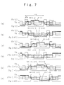
- FIGs. 7 (a) to 7(b) are signal waveform charts of the liquid crystal display panel according to the embodiment.
- FIG. 7(a) is a signal waveform chart at the pixel (i, j) .
- FIG. 7(b) is a signal waveform chart at the pixel (i+1, j).
- FIG. 7(c) is a signal waveform chart at the pixel (i+2, j).
- FIG. 7(d) is a signal waveform chart at a pixel (i, j+1).
- FIG. 7(e) is a signal waveform chart at a pixel (i+1, j+1).
- FIG. 7(f) is a signal waveform chart at a pixel (i+2, j+1).
- 1H represents a horizontal scanning period
- 1V represents a vertical scanning period
- Vc represents a counter signal
- Vg represents a scanning signal
- Vs represents an image signal
- Vd represents the potential of the pixel electrode 3
- Vf represents a modulating signal
- Vge+ represents a positive modulating voltage
- Vge- represents a negative modulating voltage.
- the application period of the modulating voltages Vge+ and Vge- is shifted by the 1H period between FIGs. 7(a) to (c) and 7(d) to 7(f).
- the auxiliary capacitance 5 of, for example, the pixel (i, j) in the i-th row is connected to the modulating electrode 8 in the i-th row
- the auxiliary capacitance 5 of, for example, the pixel (i, j+1) in the i-th row is connected to the modulating electrode 8 in the (i+1)-th row.
- the modulating electrode 8 in the (i+1)-th row is the modulating electrode 8 connected to the auxiliary capacitance 5 of the pixel (i+1, j) in the (i+1)-th row among the pixels in the j-th column.
- a common modulating electrode 8 is used as the auxiliary capacitances of pixels in rows different from each other by one row, so that a shift of the 1H period is caused during the application period of the modulating voltages Vge+ and Vge-.
- this does not cause a large problem because it is a shift of the 1H period during the 1V period.
- the image signal Vs(j) is supplied to the pixel electrode 3 serving as one of the electrodes of the liquid crystal capacitance 4 and the auxiliary capacitance 5, so that a predetermined voltage is reached.
- the scanning signal Vg(i) becomes off, it is attempted to maintain the voltage for the 1V period; however, since the auxiliary capacitance 5 is connected to the modulating electrode 8, when the modulating signal Vf(i) changes to the positive modulating voltage Vge+ or to the negative modulating voltage Vge-, the potential Vd(i, j) of the pixel electrode 3 changes accordingly.
- an effective voltage as well as the image signal Vs(j) is applied to the liquid crystal capacitance 4. The same is performed at the pixel (i+1, j) and at the pixel (i+2, j), etc.
- a reversed image signal/Vs(j+1) is supplied to the pixel electrode 3 serving as one of the electrodes of the liquid crystal capacitance 4 and the auxiliary capacitance 5, so that a predetermined voltage is reached.
- the modulating electrode 8 for applying the modulating signal Vf separately from the scanning electrode 7
- the amplitude of the scanning signal Vg output from the output IC is greatly reduced and the level output is binary, so that the area of the IC chip is greatly reduced.
- the cost of the IC is greatly reduced.
- the load capacitance of the scanning electrode 7 is reduced, so that the width of the scanning electrode 7 can be reduced to significantly improve the numerical aperture.
- the auxiliary capacitance 5 connected to the pixel electrode 3 is formed between the pixel electrode 3 and a modulating electrode 8 which differs for each column and the polarity of the image signal Vs applied to the signal electrodes 9 in odd-numbered columns and that applied to the electrodes 9 in even-numbered columns are opposite to each other, the potentials Vd of the pixel electrodes 3 are swung so as to cancel each other through adjoining signal electrode-pixel electrode capacitances Csd 1 and Csd 2 , so that the potentials Vd of the pixel electrodes 3 are not swung but become stable. As a result, crosstalk disappears and the display quality is significantly improved.
- the present invention can be embodied when these signals are all generated in an incorporated IC and supplied or are separately generated in an external IC and supplied.
- a modulating voltage for modulating the potential of a pixel electrode through an auxiliary capacitance is superimposed on a scanning signal and applied to a scanning electrode.
- modulating electrodes for applying a modulating voltage are provided separately from the scanning electrodes. Consequently, the amplitude of the scanning signal output from the output IC so as to be applied to the scanning electrode is greatly reduced and the level output is binary, so that the area of the IC chip is greatly reduced. As a result, the cost of the IC is greatly reduced.
- the load capacitance of the scanning electrode is reduced, so that the width of the scanning electrode can be reduced to significantly improve the numerical aperture.
Claims (3)
- Flüssigkristallanzeige, bei der eine Vielzahl von Pixelelektroden (3) in m Zeilen und in n Spalten auf einem lichtdurchlässigen Substrat angeordnet sind, m Zeilen von Abtastelektroden (7) und n Spalten von Signalelektroden (9) senkrecht zwischen der Vielzahl von Pixelelektroden angeordnet sind, ein Dünnfilmtransistor (2), bei dem eine Gate-Elektrode mit einer Abtastelektrode in einer i-ten Zeile verbunden ist, wobei i eine ganze Zahl zwischen 1 und m ist, eine Source-Elektrode mit einer Signalelektrode in einer j-ten Spalte verbunden ist, wobei j eine ganze Zahl zwischen 1 und n ist, und eine Drain-Elektrode mit einer Pixelelektrode in einer i-ten Zeile in der j-ten Spalte bei jeder Kreuzung der Abtastelektrode mit der Signalelektrode angeordnet ist, eine Gegenlektrode (6), die gegenüber der Pixelelektrode angeordnet ist, mit Flüssigkristall dazwischen angeordnet ist, und bei der eine Modulationselektrodenanordnung vorgesehen ist, zwischen der und den Pixelelektroden zusätzliche Kondensatoren (5) gebildet sind,
dadurch gekennzeichnet, daß die folgenden Modulationselektroden (8) vorgesehen sind: eine Modulationselektrode in einer ersten Zeile, zwischen der und der Pixelelektrode in der ersten Zeile in einer p-ten Spalte, wobei p ungeradzahlig oder geradzahlig ist als eine Zahl zwischen 1 und n, eine Zusatzkapazitanz gebildet ist; eine Modulationselektrode in einer k-ten Zeile, zwischen der und der Pixelelektrode in einer k-ten Zeile in der p-ten Spalte, wobei k eine ganze Zahl zwischen 2 und m ist, und die (k-1)-te Zeile in einer q-ten Spalte, wobei q eine andere ganze Zahl als p zwischen 1 und n ist, die Zusatzkapazitanz gebildet ist; und eine Modulationselektrode in einer (m+1)-ten Zeile zwischen der Pixelelektrode in der m-ten Zeile in der q-ten Spalte der Zusatzkapazitanz gebildet ist. - Flüssigkristallanzeige nach Anspruch 1, bei der die Modulationselektroden in der ersten bis zur (m+1)-ten Zeile gebildet sind unter Verwendung eines lichtdurchlässigen leitfähigen Materials, wobei die Modulationselektrode in der ersten Zeile vorgesehen ist zwischen der Pixelelektrode in der ersten Zeile in der p-ten Spalte und dem lichtdurchlässigen Substrat mit einem lichtdurchlässigen Isolationsfilm zwischen der Pixelelektrode in der ersten Zeile in der p-ten Spalte und der Modulationselektrode in der ersten Zeile, wobei die Modulationselektrode in der k-ten Zeile vorgesehen ist zwischen den Pixelelektroden in der k-ten Zeile in der p-ten Spalte und in der (k-1)-ten Zeile in der q-ten Spalte und dem lichtdurchlässigen Substrat mit dem lichtdurchlässigen Isolationsfilm zwischen den Pixelelektroden in der k-ten Zeile in der p-ten Spalte und in der (k-1)-ten Zeile in der q-ten Spalte und der Modulationselektrode in der k-ten Zeile, und bei der die Modulationselektrode in der (m+1)-ten Zeile zwischen der Pixelelektrode vorgesehen ist in der m-ten Zeile in der q-ten Spalte und das lichtdurchlässige Substrat mit dem lichtdurchlässigen Isolationsfilm zwischen der Pixelelektrode in der m-ten Zeile in der q-ten Spalte und der Modulationselektrode in der (m+1)-ten Zeile.
- Verfahren zum Steuern der Flüssigkristallanzeige nach Anspruch 1 oder 2, bei dem ein Potential der Pixelelektrode gesteuert wird durch die Zusatzkapazitanz durch Liefern von Bildsignalen an die Signalelektroden, wobei die Polarität der Bildsignale bei jeder Spalte der n Spalten der Signalelektroden umgepolt ist, wobei die Polarität des an jede Signalelektrode angelegten Bildsignals bei jeder Horizontalabtastperiode umgepolt ist, und durch Anlegen einer positiven Modulationsspannung und einer negativen Modulationsspannung an jede Modulationselektrode.
Applications Claiming Priority (3)
| Application Number | Priority Date | Filing Date | Title |
|---|---|---|---|
| JP15690097 | 1997-06-13 | ||
| JP156900/97 | 1997-06-13 | ||
| JP15690097 | 1997-06-13 |
Publications (3)
| Publication Number | Publication Date |
|---|---|
| EP0907159A2 EP0907159A2 (de) | 1999-04-07 |
| EP0907159A3 EP0907159A3 (de) | 1999-06-09 |
| EP0907159B1 true EP0907159B1 (de) | 2001-09-12 |
Family
ID=15637860
Family Applications (1)
| Application Number | Title | Priority Date | Filing Date |
|---|---|---|---|
| EP19980110819 Expired - Lifetime EP0907159B1 (de) | 1997-06-13 | 1998-06-12 | Flüssigkristallanzeigegerät mit aktiver Matrix und Steuerungsverfahren dafür |
Country Status (4)
| Country | Link |
|---|---|
| EP (1) | EP0907159B1 (de) |
| KR (1) | KR19990006945A (de) |
| DE (1) | DE69801627T2 (de) |
| TW (1) | TW388857B (de) |
Families Citing this family (3)
| Publication number | Priority date | Publication date | Assignee | Title |
|---|---|---|---|---|
| TW521241B (en) * | 1999-03-16 | 2003-02-21 | Sony Corp | Liquid crystal display apparatus, its driving method, and liquid crystal display system |
| JP2001188217A (ja) | 1999-10-20 | 2001-07-10 | Sharp Corp | アクティブマトリクス型液晶表示装置およびその駆動方法ならびに製造方法 |
| US8115757B2 (en) | 2007-09-11 | 2012-02-14 | Sharp Kabushiki Kaisha | Display device, it's driving circuit, and driving method |
Family Cites Families (6)
| Publication number | Priority date | Publication date | Assignee | Title |
|---|---|---|---|---|
| JP2568659B2 (ja) * | 1988-12-12 | 1997-01-08 | 松下電器産業株式会社 | 表示装置の駆動方法 |
| EP0535954B1 (de) * | 1991-10-04 | 1998-04-15 | Kabushiki Kaisha Toshiba | Flüssigkristallanzeigegerät |
| JP3529153B2 (ja) * | 1993-03-04 | 2004-05-24 | 三星電子株式会社 | 液晶表示装置及びその製造方法 |
| EP1463028A2 (de) * | 1993-04-22 | 2004-09-29 | Matsushita Electric Industrial Co., Ltd. | Anzeigevorrichtung und Projektionsanzeigeeinrichtung mit Benutzung derselben |
| JP2797972B2 (ja) * | 1994-06-28 | 1998-09-17 | 日本電気株式会社 | アクティブマトリクス型液晶表示装置 |
| JP3194873B2 (ja) * | 1996-10-15 | 2001-08-06 | 松下電器産業株式会社 | アクティブマトリックス型液晶表示装置およびその駆動方法 |
-
1998
- 1998-06-06 TW TW87109010A patent/TW388857B/zh not_active IP Right Cessation
- 1998-06-12 KR KR1019980022042A patent/KR19990006945A/ko not_active Application Discontinuation
- 1998-06-12 EP EP19980110819 patent/EP0907159B1/de not_active Expired - Lifetime
- 1998-06-12 DE DE1998601627 patent/DE69801627T2/de not_active Expired - Fee Related
Also Published As
| Publication number | Publication date |
|---|---|
| KR19990006945A (ko) | 1999-01-25 |
| DE69801627T2 (de) | 2002-04-18 |
| EP0907159A2 (de) | 1999-04-07 |
| DE69801627D1 (de) | 2001-10-18 |
| TW388857B (en) | 2000-05-01 |
| EP0907159A3 (de) | 1999-06-09 |
Similar Documents
| Publication | Publication Date | Title |
|---|---|---|
| EP0622772B1 (de) | Verfahren und Vorrichtung zum Eliminieren des Übersprechens in einer Flüssigkristall-Anzeigeeinrichtung mit aktiver Matrix | |
| EP0535954B1 (de) | Flüssigkristallanzeigegerät | |
| TWI397734B (zh) | 液晶顯示器及其驅動方法 | |
| US7079102B2 (en) | Driving method for liquid crystal display apparatus and liquid crystal display apparatus | |
| US20090102824A1 (en) | Active matrix substrate and display device using the same | |
| US20070273677A1 (en) | Driving device and display apparatus having the same | |
| US20050041488A1 (en) | Electro-optical device, method for driving the electro-optical device, and electronic apparatus including the electro-optical device | |
| CN101512628A (zh) | 有源矩阵基板及具备该有源矩阵基板的显示装置 | |
| JPH06265846A (ja) | アクティブマトリクス型液晶表示装置及びその駆動方法 | |
| KR100628937B1 (ko) | 능동 매트릭스 액정 디스플레이 장치 | |
| US6130654A (en) | Driving method of a liquid crystal display device | |
| JP3031295B2 (ja) | アクティブマトリクス型液晶表示装置 | |
| US20050046620A1 (en) | Thin film transistor LCD structure and driving method thereof | |
| US20040080679A1 (en) | Liquid crystal display and fabricating method thereof | |
| US7728804B2 (en) | Liquid crystal display device and driving method thereof | |
| KR100354795B1 (ko) | 매트릭스형 표시 장치 | |
| US9140942B2 (en) | Liquid crystal display device and multi-display system | |
| US6927752B2 (en) | Plane display element | |
| US6636196B2 (en) | Electro-optic display device using a multi-row addressing scheme | |
| EP0907159B1 (de) | Flüssigkristallanzeigegerät mit aktiver Matrix und Steuerungsverfahren dafür | |
| US6452580B1 (en) | Active matrix liquid crystal display device | |
| KR100464206B1 (ko) | 2-도트인버젼방식 액정표시소자 | |
| JPH1164893A (ja) | 液晶表示パネルおよびその駆動方法 | |
| US20050017937A1 (en) | Active matrix driver | |
| JP3297335B2 (ja) | 液晶表示装置 |
Legal Events
| Date | Code | Title | Description |
|---|---|---|---|
| PUAI | Public reference made under article 153(3) epc to a published international application that has entered the european phase |
Free format text: ORIGINAL CODE: 0009012 |
|
| 17P | Request for examination filed |
Effective date: 19980612 |
|
| AK | Designated contracting states |
Kind code of ref document: A2 Designated state(s): DE FR GB |
|
| AX | Request for extension of the european patent |
Free format text: AL;LT;LV;MK;RO;SI |
|
| PUAL | Search report despatched |
Free format text: ORIGINAL CODE: 0009013 |
|
| AK | Designated contracting states |
Kind code of ref document: A3 Designated state(s): AT BE CH CY DE DK ES FI FR GB GR IE IT LI LU MC NL PT SE |
|
| AX | Request for extension of the european patent |
Free format text: AL;LT;LV;MK;RO;SI |
|
| RIC1 | Information provided on ipc code assigned before grant |
Free format text: 6G 09G 3/36 A, 6G 02F 1/136 B |
|
| RAP1 | Party data changed (applicant data changed or rights of an application transferred) |
Owner name: MATSUSHITA ELECTRIC INDUSTRIAL CO., LTD. |
|
| K1C3 | Correction of patent application (complete document) published |
Effective date: 19990609 |
|
| AKX | Designation fees paid |
Free format text: DE FR GB |
|
| 17Q | First examination report despatched |
Effective date: 20000208 |
|
| GRAG | Despatch of communication of intention to grant |
Free format text: ORIGINAL CODE: EPIDOS AGRA |
|
| GRAG | Despatch of communication of intention to grant |
Free format text: ORIGINAL CODE: EPIDOS AGRA |
|
| GRAH | Despatch of communication of intention to grant a patent |
Free format text: ORIGINAL CODE: EPIDOS IGRA |
|
| GRAH | Despatch of communication of intention to grant a patent |
Free format text: ORIGINAL CODE: EPIDOS IGRA |
|
| GRAA | (expected) grant |
Free format text: ORIGINAL CODE: 0009210 |
|
| AK | Designated contracting states |
Kind code of ref document: B1 Designated state(s): DE FR GB |
|
| REF | Corresponds to: |
Ref document number: 69801627 Country of ref document: DE Date of ref document: 20011018 |
|
| REG | Reference to a national code |
Ref country code: GB Ref legal event code: IF02 |
|
| ET | Fr: translation filed | ||
| PLBE | No opposition filed within time limit |
Free format text: ORIGINAL CODE: 0009261 |
|
| STAA | Information on the status of an ep patent application or granted ep patent |
Free format text: STATUS: NO OPPOSITION FILED WITHIN TIME LIMIT |
|
| 26N | No opposition filed | ||
| REG | Reference to a national code |
Ref country code: GB Ref legal event code: 732E |
|
| REG | Reference to a national code |
Ref country code: FR Ref legal event code: TP |
|
| PGFP | Annual fee paid to national office [announced via postgrant information from national office to epo] |
Ref country code: DE Payment date: 20080619 Year of fee payment: 11 |
|
| PGFP | Annual fee paid to national office [announced via postgrant information from national office to epo] |
Ref country code: FR Payment date: 20080617 Year of fee payment: 11 |
|
| PGFP | Annual fee paid to national office [announced via postgrant information from national office to epo] |
Ref country code: GB Payment date: 20080618 Year of fee payment: 11 |
|
| GBPC | Gb: european patent ceased through non-payment of renewal fee |
Effective date: 20090612 |
|
| REG | Reference to a national code |
Ref country code: FR Ref legal event code: ST Effective date: 20100226 |
|
| PG25 | Lapsed in a contracting state [announced via postgrant information from national office to epo] |
Ref country code: FR Free format text: LAPSE BECAUSE OF NON-PAYMENT OF DUE FEES Effective date: 20090630 |
|
| PG25 | Lapsed in a contracting state [announced via postgrant information from national office to epo] |
Ref country code: GB Free format text: LAPSE BECAUSE OF NON-PAYMENT OF DUE FEES Effective date: 20090612 |
|
| PG25 | Lapsed in a contracting state [announced via postgrant information from national office to epo] |
Ref country code: DE Free format text: LAPSE BECAUSE OF NON-PAYMENT OF DUE FEES Effective date: 20100101 |