EP0905972A2 - Rücklauftransformator - Google Patents
Rücklauftransformator Download PDFInfo
- Publication number
- EP0905972A2 EP0905972A2 EP98117382A EP98117382A EP0905972A2 EP 0905972 A2 EP0905972 A2 EP 0905972A2 EP 98117382 A EP98117382 A EP 98117382A EP 98117382 A EP98117382 A EP 98117382A EP 0905972 A2 EP0905972 A2 EP 0905972A2
- Authority
- EP
- European Patent Office
- Prior art keywords
- flyback transformer
- circuit
- primary winding
- voltage
- winding
- Prior art date
- Legal status (The legal status is an assumption and is not a legal conclusion. Google has not performed a legal analysis and makes no representation as to the accuracy of the status listed.)
- Withdrawn
Links
- 238000004804 winding Methods 0.000 claims abstract description 67
- 239000011162 core material Substances 0.000 description 34
- 239000003990 capacitor Substances 0.000 description 11
- 230000003247 decreasing effect Effects 0.000 description 10
- 238000010276 construction Methods 0.000 description 6
- 238000010586 diagram Methods 0.000 description 4
- 238000005259 measurement Methods 0.000 description 4
- 238000000034 method Methods 0.000 description 3
- 230000003071 parasitic effect Effects 0.000 description 3
- RYGMFSIKBFXOCR-UHFFFAOYSA-N Copper Chemical compound [Cu] RYGMFSIKBFXOCR-UHFFFAOYSA-N 0.000 description 2
- 230000033228 biological regulation Effects 0.000 description 2
- 230000001276 controlling effect Effects 0.000 description 2
- 229910052802 copper Inorganic materials 0.000 description 2
- 239000010949 copper Substances 0.000 description 2
- 238000012986 modification Methods 0.000 description 2
- 230000004048 modification Effects 0.000 description 2
- 238000007493 shaping process Methods 0.000 description 2
- 230000000052 comparative effect Effects 0.000 description 1
- 230000007423 decrease Effects 0.000 description 1
- 230000000694 effects Effects 0.000 description 1
- 238000002474 experimental method Methods 0.000 description 1
- 230000005669 field effect Effects 0.000 description 1
- 238000009499 grossing Methods 0.000 description 1
- 230000017525 heat dissipation Effects 0.000 description 1
- 239000000463 material Substances 0.000 description 1
- 229910044991 metal oxide Inorganic materials 0.000 description 1
- 150000004706 metal oxides Chemical class 0.000 description 1
- 230000001105 regulatory effect Effects 0.000 description 1
- 239000004065 semiconductor Substances 0.000 description 1
Images


Classifications
-
- H—ELECTRICITY
- H04—ELECTRIC COMMUNICATION TECHNIQUE
- H04N—PICTORIAL COMMUNICATION, e.g. TELEVISION
- H04N3/00—Scanning details of television systems; Combination thereof with generation of supply voltages
- H04N3/10—Scanning details of television systems; Combination thereof with generation of supply voltages by means not exclusively optical-mechanical
- H04N3/16—Scanning details of television systems; Combination thereof with generation of supply voltages by means not exclusively optical-mechanical by deflecting electron beam in cathode-ray tube, e.g. scanning corrections
- H04N3/18—Generation of supply voltages, in combination with electron beam deflecting
- H04N3/185—Maintaining DC voltage constant
Definitions
- the present invention relates to a flyback transformer which generates a high voltage for a color CRT display.
- a flyback transformer is used as a high-voltage generation circuit for generating an anode voltage or the like for a color CRT display for use in television receivers and computer monitors.
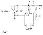
- FIG. 7 An example of a conventional high-voltage generation circuit is shown in Fig. 7.
- a driving power source 3 is connected between one end of a primary winding 2 and a ground.
- a transistor 11 as a switching element is connected in series to the other end of the primary winding 2, with each of a damper diode 5 and a resonance capacitor 6 being connected in parallel to this switching element.
- the high-voltage end of a secondary winding 7 of a flyback transformer 1 is connected to the anode of a CRT through a high-voltage rectifier diode 8.
- a control circuit inputs a voltage divided by resistors 15 and 16 and compares it with a reference voltage, and controls the voltage of the driving power source 3 so that the high output voltage is stabilized.
- the reactive energy of a flyback transformer is increased, a resonance frequency is tuned to ninth-order, thirteenth-order, or other harmonic in order to bring the waveform of the flyback pulse close to that of a rectangular wave, so that the regulation characteristics of the flyback transformer itself are improved.
- a flyback transformer in which improvements are made on the power circuit is disclosed in Japanese Unexamined Patent Publication Nos. 2-222374 and 8-256476.
- the former discloses that a driving voltage which is supplied to the primary winding of the flyback transformer is PWM-controlled in synchronization with a horizontal driving signal in accordance with an output voltage.
- the latter discloses that a high output voltage is stabilized by directly PWM-controlling the ON period of a switching element which controls the ON/OFF of the primary-winding current in synchronization with a horizontal driving signal in accordance with an output voltage.
- These power circuits have high-speed response because the primary side is controlled in synchronization with a horizontal driving signal without using a smoothing circuit, rather than controlling the driving voltage in a DC manner as in the conventional power circuit shown in Fig. 7.
- An object of the present invention is to reduce the size of a flyback transformer which is connected to a power circuit comprising a circuit for performing negative feedback control of a circuit which disconnects electric current flowing through a primary winding in synchronization with a horizontal driving signal in accordance with an output voltage.
- a flyback transformer for a color CRT display which is connected to a power circuit comprising: a circuit which disconnects electric current flowing through a primary winding; and a circuit which performs negative feedback control of the circuit in synchronization with a horizontal driving signal in accordance with an output voltage, wherein the turn ratio of the secondary winding to the primary winding is set to 80 or more.
- the circuit which performs negative feedback of the primary side preferably PWM-controls the ON period of the switching element in accordance with an output voltage.
- the diameter of a core around which the primary winding and the secondary winding are wound is preferably 10 mm or less.
- the color CRT display is preferably a multiscan-compatible display in which the highest frequency of the horizontal driving signal is 115 kHz or lower.
- reference numeral 1 denotes a flyback transformer.
- a driving power source 3 is connected to one end of a primary winding 2 of this flyback transformer 1, the drain of an MOS-FET (metal oxide semiconductor field-effect transistor) (hereinafter simply referred to as a "transistor") 11 as a switching element is connected to the other end of the primary winding 2, the source thereof being grounded.
- MOS-FET metal oxide semiconductor field-effect transistor
- a diode 26 is connected in series to the transistor 11.
- One end of a resonance capacitor 6 is connected to one end of the primary winding 2, the cathode of a diode 12 is connected to the other end thereof, and the anode of the diode 12 is connected to the ground.
- the anode of a diode 13 is connected to the connection portion of the diode 12 and the resonance capacitor 6, and the cathode of the diode 13 is connected between the primary winding 2 and the driving power source 3.
- the low-voltage end of the secondary winding 7 of the flyback transformer 1 is connected to an ABL (automatic brightness control circuit), and voltage-division resistors 15 and 16 are connected to the high-voltage end.
- ABL automatic brightness control circuit
- This divided voltage is applied to the non-inversion input terminal of an operational amplifier 17.
- the reference voltage of a reference power source 18 is applied to the inversion input terminal of the operational amplifier 17.
- This operational amplifier 17, together with the resistor connected thereto, constitutes an error amplifier circuit.
- the output signal of the operational amplifier 17 is connected to the inversion input terminal of a comparator 20, and a signal from a waveform shaping circuit 21 is applied to the non-inversion input terminal of the comparator 20.
- the waveform shaping circuit 21 integrates the horizontal driving signal (HD signal) in order to generate a ramp waveform.
- a driving circuit 22 performs switching of the transistor 11 in accordance with an output signal of the comparator 20.
- Fig. 2 shows waveform charts of each section of the circuit shown in Fig. 1. The operation of this power circuit will now be described with reference to Figs. 1 and 2.
- the transistor 11 is turned on at time t0, electric current flows from the driving power source 3 side, through the primary winding 2, through the transistor 11, to the ground.
- the electric current which flows through this primary winding 2 increases with time as shown at the bottom of Fig. 2, and accumulates as electromagnetic energy in the primary winding 2.
- the driving circuit 22 turns on/off the transistor 11 in accordance with a control signal from the control circuit. This causes the transistor to be turned on at a predetermined ON time in a cycle of a fixed horizontal driving signal (HD signal). Since this ON time is negative-feedback-controlled so that the input potential difference of the operational amplifier 17 becomes 0, the output voltage is stabilized.
- Fig. 3 shows another example of a power circuit in which a high output voltage is stabilized by PWM-controlling the driving power-source voltage.
- a switching transistor 31 is connected between one end of the primary winding 2 of the flyback transformer 1 and the driving power source 3.
- the control circuit inputs a voltage divided by the resistors 15 and 16 and performs on/off control of the switching transistor 31 in synchronization with a horizontal driving signal (HD signal). More specifically, by performing negative feedback control so that the less the detected value of the output voltage is decreased from the reference voltage, the longer the ON time of the switching transistor 31 takes, the output voltage is stabilized.
- HD signal horizontal driving signal
- the switching transistor 31 Since the switching transistor 31 is controlled so that it is shut off before the flyback period starts, that is, in the ON period of the transistor 11, after the switching transistor 31 is turned off, collector current of the transistor 11 flows through a diode 32.
- the control circuit controls the ON time of the switching transistor 31 so that the voltage detected by the resistance division circuit of the resistors 15 and 16 becomes equal to the reference voltage. As a result, the output voltage is stabilized.
- the present invention is designed to reduce the size of a flyback transformer without regulating the flyback transformer itself and also to reduce the size of the entire power circuit which generates a high voltage by utilizing the regulation characteristics of the power circuit itself.
- Vcp the peak voltage across both ends of the transistor which turns on/off the primary-winding current
- E B the driving power voltage
- ton the ON time of the transistor
- L the primary inductance
- I P the peak current of the primary winding
- n the turn ratio of the secondary winding to the primary winding
- Hv is the output voltage.
- the current loss (called “copper loss”) is expressed by a function of an effective current value of the primary winding. Therefore, the smaller I P is, the smaller the copper loss.
- I P can be decreased by increasing the turn ratio n of the secondary winding to the primary winding, making it possible to suppress the entire loss.
- Another example of loss in a flyback transformer includes dielectric loss. This is determined by a geometrical structure, such as a winding structure of windings around the core, and the greater the turn ratio, the greater this dielectric loss. That is, there is a trade-off between the core loss and the dielectric loss.
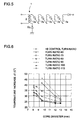
- the relationship between the turn ratio n and the loss of the entire flyback transformer is shown in Fig. 4. As shown in the Figure, the greater the turn ratio n, the less the core loss Pc is decreased and the more the dielectric loss Pe is increased. However, unlike the case of Pc, the dielectric loss Pe can be reduced to some extent without enlarging the entire flyback transformer.
- Fig. 5 shows a circuit diagram for the construction of a flyback transformer suitable for reducing dielectric loss.
- the secondary winding of the flyback transformer 1 is formed to be a multilayered winding of five layers indicated by 7a to 7e. This is such that secondary windings are each wound around the cylindrical winding core; these are overlaid in five layers and diodes are connected between the layers. Furthermore, a diode Do is inserted into the low voltage end of the secondary winding.
- a diode is inserted into at each position at which the secondary winding is divided, and further, a diode is inserted into the low voltage end side, thereby the sharing of the voltage at each section of the secondary winding is performed.
- This causes the voltage gradient to be low overall, and the dielectric loss is decreased. For this reason, as indicated by the broken line shown in Fig. 4, the turn ratio n at which the loss P of the entire flyback transformer is minimized can be increased.
- Ib is the DC component of the primary-winding current
- Ip is the peak current (zero-peak AC components) of the primary winding
- Vcp is the peak voltage across both ends of the transistor
- Tr is the flyback pulse width
- Ton is the transistor ON time
- ⁇ T is an increase in temperature of the core in an atmosphere of 60°C. All of these are examples applied to the power circuit shown in Fig. 1. It can be seen from this result that the more the turn ratio n is increased from 70 to 110, the smaller the temperature increase ⁇ T of the core becomes. Since the greater the turn ratio n is, the less Ip is decreased in the manner described above, ⁇ T is decreased.
- ⁇ T be suppressed to 35°C or less in an atmosphere of 60°C.
- Fig. 6 results are shown in which the core temperature increase ⁇ T was measured when the turn ratio n was varied and the core diameter was varied.
- "+B control" in the Figure is a conventional control method shown in Fig. 7, which is an example in which a conventional flyback transformer, whose turn ratio n is 60, is used, and is shown here as a comparative example.
- Fig. 7 is an example in which a conventional flyback transformer, whose turn ratio n is 60, is used, and is shown here as a comparative example.
- ⁇ T can be suppressed to 35°C or less in either case, but when the core diameter is 9.5 mm, if the turn ratio n is 60, ⁇ T exceeds 35°C. Therefore, the conventional flyback transformer ordinarily cannot be used.
- the temperature increase is increased further under the +B control, and the conventional flyback transformer cannot be used.
- ⁇ T is increased slightly more than the above-described measurement results.
- the core diameter at 10 mm and setting the turn ratio at 80, ⁇ T can be suppressed to 35°C or less. Therefore, if the turn ratio is set at 80 or more, even if a core having a diameter of 10 mm or less is used, the flyback transformer can be applied to a multiscan-compatible color CRT display in which the highest frequency of the horizontal driving signal is 115 kHz.
- the on/off control of the primary-winding current of the flyback transformer can be performed by using a single switching element, the number of parts can be reduced, making it possible to reduce the size of the entire power circuit as well as the flyback transformer of the present invention.
- the present invention by limiting the diameter of the core, it is possible to reduce the size of the entire flyback transformer within a fixed temperature increase range.
Landscapes
- Engineering & Computer Science (AREA)
- Multimedia (AREA)
- Signal Processing (AREA)
- Dc-Dc Converters (AREA)
- Details Of Television Scanning (AREA)
- Coils Or Transformers For Communication (AREA)
Applications Claiming Priority (3)
| Application Number | Priority Date | Filing Date | Title |
|---|---|---|---|
| JP264027/97 | 1997-09-29 | ||
| JP9264027A JPH11103574A (ja) | 1997-09-29 | 1997-09-29 | フライバックトランス |
| JP26402797 | 1997-09-29 |
Publications (2)
| Publication Number | Publication Date |
|---|---|
| EP0905972A2 true EP0905972A2 (de) | 1999-03-31 |
| EP0905972A3 EP0905972A3 (de) | 2000-12-27 |
Family
ID=17397543
Family Applications (1)
| Application Number | Title | Priority Date | Filing Date |
|---|---|---|---|
| EP98117382A Withdrawn EP0905972A3 (de) | 1997-09-29 | 1998-09-14 | Rücklauftransformator |
Country Status (4)
| Country | Link |
|---|---|
| EP (1) | EP0905972A3 (de) |
| JP (1) | JPH11103574A (de) |
| KR (1) | KR100303637B1 (de) |
| TW (1) | TW395076B (de) |
Cited By (2)
| Publication number | Priority date | Publication date | Assignee | Title |
|---|---|---|---|---|
| WO2001005193A1 (en) * | 1999-07-07 | 2001-01-18 | Koninklijke Philips Electronics N.V. | Flyback converter as led driver |
| US7030572B2 (en) | 2002-12-03 | 2006-04-18 | Lumileds Lighting U.S., Llc | Lighting arrangement |
Families Citing this family (2)
| Publication number | Priority date | Publication date | Assignee | Title |
|---|---|---|---|---|
| JP2000152023A (ja) | 1998-09-04 | 2000-05-30 | Matsushita Electric Ind Co Ltd | 高圧発生装置 |
| JP6259247B2 (ja) * | 2013-10-09 | 2018-01-10 | 浜松ホトニクス株式会社 | 共振型スイッチング電源回路 |
Family Cites Families (2)
| Publication number | Priority date | Publication date | Assignee | Title |
|---|---|---|---|---|
| JP3097315B2 (ja) * | 1992-05-15 | 2000-10-10 | 株式会社村田製作所 | 高電圧発生回路 |
| JP2531008B2 (ja) * | 1992-09-25 | 1996-09-04 | 株式会社村田製作所 | 共振型電源回路 |
-
1997
- 1997-09-29 JP JP9264027A patent/JPH11103574A/ja active Pending
-
1998
- 1998-09-08 TW TW087114911A patent/TW395076B/zh not_active IP Right Cessation
- 1998-09-14 EP EP98117382A patent/EP0905972A3/de not_active Withdrawn
- 1998-09-25 KR KR1019980039991A patent/KR100303637B1/ko not_active Expired - Fee Related
Cited By (2)
| Publication number | Priority date | Publication date | Assignee | Title |
|---|---|---|---|---|
| WO2001005193A1 (en) * | 1999-07-07 | 2001-01-18 | Koninklijke Philips Electronics N.V. | Flyback converter as led driver |
| US7030572B2 (en) | 2002-12-03 | 2006-04-18 | Lumileds Lighting U.S., Llc | Lighting arrangement |
Also Published As
| Publication number | Publication date |
|---|---|
| TW395076B (en) | 2000-06-21 |
| JPH11103574A (ja) | 1999-04-13 |
| KR19990030162A (ko) | 1999-04-26 |
| EP0905972A3 (de) | 2000-12-27 |
| KR100303637B1 (ko) | 2001-11-14 |
Similar Documents
| Publication | Publication Date | Title |
|---|---|---|
| EP0605752A2 (de) | Schaltnetzteil | |
| US5383106A (en) | Regenerative control type switching power source device | |
| US5640310A (en) | Current resonance type switching power source | |
| US4745535A (en) | Ringing choke type DC/DC converter | |
| US4144480A (en) | High voltage generating apparatus | |
| US4968106A (en) | High voltage generating apparatus for television equipment | |
| EP0905972A2 (de) | Rücklauftransformator | |
| US6765809B2 (en) | Power source circuit having regulated primary current | |
| KR100294733B1 (ko) | 편향 고압 일체형 전원장치 | |
| EP0128223B1 (de) | Stabilisierungsschaltung für hochspannung | |
| US5939844A (en) | High-frequency horizontal deflection/high-voltage generation apparatus for cathode ray tube | |
| CA2214217C (en) | Switching power supply apparatus | |
| JPS63228967A (ja) | 共振型スイツチング電源 | |
| JP3258620B2 (ja) | スイッチング電源装置 | |
| JP2581034B2 (ja) | マルチスキヤンテレビジヨン受像機用スイツチング電源装置 | |
| EP0319011B1 (de) | Hochspannungserzeuger für Fernsehgeräte | |
| JP2856510B2 (ja) | 高圧安定化電源装置 | |
| KR820001669B1 (ko) | 스위치형 전압변환기 | |
| JPS63117662A (ja) | 高電圧発生回路 | |
| JP2563363B2 (ja) | フライバックトランス装置 | |
| KR800000857B1 (ko) | 고압발생장치 | |
| KR920007135Y1 (ko) | 전원 공급장치의 안정화회로 | |
| JPH03159476A (ja) | 高圧安定化電源装置 | |
| JPS6031325Y2 (ja) | 水平出力装置 | |
| JP2000013633A (ja) | 高圧回路 |
Legal Events
| Date | Code | Title | Description |
|---|---|---|---|
| PUAI | Public reference made under article 153(3) epc to a published international application that has entered the european phase |
Free format text: ORIGINAL CODE: 0009012 |
|
| 17P | Request for examination filed |
Effective date: 19980914 |
|
| AK | Designated contracting states |
Kind code of ref document: A2 Designated state(s): DE FR GB |
|
| AX | Request for extension of the european patent |
Free format text: AL;LT;LV;MK;RO;SI |
|
| PUAL | Search report despatched |
Free format text: ORIGINAL CODE: 0009013 |
|
| AK | Designated contracting states |
Kind code of ref document: A3 Designated state(s): AT BE CH CY DE DK ES FI FR GB GR IE IT LI LU MC NL PT SE |
|
| AX | Request for extension of the european patent |
Free format text: AL;LT;LV;MK;RO;SI |
|
| AKX | Designation fees paid |
Free format text: DE FR GB |
|
| STAA | Information on the status of an ep patent application or granted ep patent |
Free format text: STATUS: THE APPLICATION HAS BEEN WITHDRAWN |
|
| 18W | Application withdrawn |
Withdrawal date: 20011109 |