EP0905723B1 - Matériaux diélectriques amorphes et condensateurs utilisant ceux-ci - Google Patents
Matériaux diélectriques amorphes et condensateurs utilisant ceux-ci Download PDFInfo
- Publication number
- EP0905723B1 EP0905723B1 EP98307232A EP98307232A EP0905723B1 EP 0905723 B1 EP0905723 B1 EP 0905723B1 EP 98307232 A EP98307232 A EP 98307232A EP 98307232 A EP98307232 A EP 98307232A EP 0905723 B1 EP0905723 B1 EP 0905723B1
- Authority
- EP
- European Patent Office
- Prior art keywords
- dielectric
- substrate
- capacitor
- composition
- films
- Prior art date
- Legal status (The legal status is an assumption and is not a legal conclusion. Google has not performed a legal analysis and makes no representation as to the accuracy of the status listed.)
- Expired - Lifetime
Links
Images

Classifications
-
- H—ELECTRICITY
- H10—SEMICONDUCTOR DEVICES; ELECTRIC SOLID-STATE DEVICES NOT OTHERWISE PROVIDED FOR
- H10P—GENERIC PROCESSES OR APPARATUS FOR THE MANUFACTURE OR TREATMENT OF DEVICES COVERED BY CLASS H10
- H10P14/00—Formation of materials, e.g. in the shape of layers or pillars
- H10P14/60—Formation of materials, e.g. in the shape of layers or pillars of insulating materials
- H10P14/69—Inorganic materials
- H10P14/692—Inorganic materials composed of oxides, glassy oxides or oxide-based glasses
- H10P14/6938—Inorganic materials composed of oxides, glassy oxides or oxide-based glasses the material containing at least one metal element, e.g. metal oxides, metal oxynitrides or metal oxycarbides
- H10P14/6939—Inorganic materials composed of oxides, glassy oxides or oxide-based glasses the material containing at least one metal element, e.g. metal oxides, metal oxynitrides or metal oxycarbides characterised by the metal
- H10P14/69397—Inorganic materials composed of oxides, glassy oxides or oxide-based glasses the material containing at least one metal element, e.g. metal oxides, metal oxynitrides or metal oxycarbides characterised by the metal the material containing two or more metal elements
-
- H—ELECTRICITY
- H10—SEMICONDUCTOR DEVICES; ELECTRIC SOLID-STATE DEVICES NOT OTHERWISE PROVIDED FOR
- H10D—INORGANIC ELECTRIC SEMICONDUCTOR DEVICES
- H10D1/00—Resistors, capacitors or inductors
- H10D1/60—Capacitors
- H10D1/68—Capacitors having no potential barriers
- H10D1/682—Capacitors having no potential barriers having dielectrics comprising perovskite structures
-
- H—ELECTRICITY
- H10—SEMICONDUCTOR DEVICES; ELECTRIC SOLID-STATE DEVICES NOT OTHERWISE PROVIDED FOR
- H10P—GENERIC PROCESSES OR APPARATUS FOR THE MANUFACTURE OR TREATMENT OF DEVICES COVERED BY CLASS H10
- H10P14/00—Formation of materials, e.g. in the shape of layers or pillars
- H10P14/60—Formation of materials, e.g. in the shape of layers or pillars of insulating materials
- H10P14/63—Formation of materials, e.g. in the shape of layers or pillars of insulating materials characterised by the formation processes
- H10P14/6326—Deposition processes
- H10P14/6328—Deposition from the gas or vapour phase
- H10P14/6329—Deposition from the gas or vapour phase using physical ablation of a target, e.g. physical vapour deposition or pulsed laser deposition
-
- H—ELECTRICITY
- H10—SEMICONDUCTOR DEVICES; ELECTRIC SOLID-STATE DEVICES NOT OTHERWISE PROVIDED FOR
- H10P—GENERIC PROCESSES OR APPARATUS FOR THE MANUFACTURE OR TREATMENT OF DEVICES COVERED BY CLASS H10
- H10P14/00—Formation of materials, e.g. in the shape of layers or pillars
- H10P14/60—Formation of materials, e.g. in the shape of layers or pillars of insulating materials
- H10P14/69—Inorganic materials
- H10P14/692—Inorganic materials composed of oxides, glassy oxides or oxide-based glasses
- H10P14/6938—Inorganic materials composed of oxides, glassy oxides or oxide-based glasses the material containing at least one metal element, e.g. metal oxides, metal oxynitrides or metal oxycarbides
- H10P14/6939—Inorganic materials composed of oxides, glassy oxides or oxide-based glasses the material containing at least one metal element, e.g. metal oxides, metal oxynitrides or metal oxycarbides characterised by the metal
- H10P14/69392—Inorganic materials composed of oxides, glassy oxides or oxide-based glasses the material containing at least one metal element, e.g. metal oxides, metal oxynitrides or metal oxycarbides characterised by the metal the material containing hafnium, e.g. HfO2
-
- H—ELECTRICITY
- H10—SEMICONDUCTOR DEVICES; ELECTRIC SOLID-STATE DEVICES NOT OTHERWISE PROVIDED FOR
- H10P—GENERIC PROCESSES OR APPARATUS FOR THE MANUFACTURE OR TREATMENT OF DEVICES COVERED BY CLASS H10
- H10P14/00—Formation of materials, e.g. in the shape of layers or pillars
- H10P14/60—Formation of materials, e.g. in the shape of layers or pillars of insulating materials
- H10P14/69—Inorganic materials
- H10P14/692—Inorganic materials composed of oxides, glassy oxides or oxide-based glasses
- H10P14/6938—Inorganic materials composed of oxides, glassy oxides or oxide-based glasses the material containing at least one metal element, e.g. metal oxides, metal oxynitrides or metal oxycarbides
- H10P14/6939—Inorganic materials composed of oxides, glassy oxides or oxide-based glasses the material containing at least one metal element, e.g. metal oxides, metal oxynitrides or metal oxycarbides characterised by the metal
- H10P14/69394—Inorganic materials composed of oxides, glassy oxides or oxide-based glasses the material containing at least one metal element, e.g. metal oxides, metal oxynitrides or metal oxycarbides characterised by the metal the material containing titanium, e.g. TiO2
-
- H—ELECTRICITY
- H10—SEMICONDUCTOR DEVICES; ELECTRIC SOLID-STATE DEVICES NOT OTHERWISE PROVIDED FOR
- H10P—GENERIC PROCESSES OR APPARATUS FOR THE MANUFACTURE OR TREATMENT OF DEVICES COVERED BY CLASS H10
- H10P14/00—Formation of materials, e.g. in the shape of layers or pillars
- H10P14/60—Formation of materials, e.g. in the shape of layers or pillars of insulating materials
- H10P14/69—Inorganic materials
- H10P14/692—Inorganic materials composed of oxides, glassy oxides or oxide-based glasses
- H10P14/6938—Inorganic materials composed of oxides, glassy oxides or oxide-based glasses the material containing at least one metal element, e.g. metal oxides, metal oxynitrides or metal oxycarbides
- H10P14/6939—Inorganic materials composed of oxides, glassy oxides or oxide-based glasses the material containing at least one metal element, e.g. metal oxides, metal oxynitrides or metal oxycarbides characterised by the metal
- H10P14/69395—Inorganic materials composed of oxides, glassy oxides or oxide-based glasses the material containing at least one metal element, e.g. metal oxides, metal oxynitrides or metal oxycarbides characterised by the metal the material containing zirconium, e.g. ZrO2
Definitions
- the invention relates to dielectric materials comprising thin, amorphous films of R-Sn-Ti-O, where R is selected from the group consisting of Zr and Hf.
- the invention has particular application for use in a capacitor of a dynamic random access memory (DRAM) device.
- DRAM dynamic random access memory
- the figure of merit being the multiple of the dielectric constant ( ⁇ ) and breakdown field (E br ) of a material.
- the dielectric constant ( ⁇ ) times the breakdown field (E br ) [MV/cm] equals its figure of merit ( ⁇ E br ) [ ⁇ C/cm 2 ].
- the figure of merit is a useful unit of measure of the efficacy of a dielectric material, as it is not dependent upon film thickness.
- a-Ta 2 O 5 amorphous tantalum pentoxide
- a-TiO x a-TiO x
- crystalline x-(Ba,Sr)TiO 3 a-Ta 2 O 5
- dielectric materials offer advantages and disadvantages.
- the relatively high dielectric constant and large figure of merit for a-TaO x films have made them of particular interest.
- dielectric films for use in integrated circuits with even higher dielectric constants (and breakdown fields), which has spurred interest in materials such as a-TiO x and x-(Ba,Sr)TiO 3 .
- R-Sn-Ti-O thin amorphous films of R-Sn-Ti-O are useful for this purpose, where R is selected from the group consisting of zirconium (Zr) and hafnium (Hf).
- Zr-Ti-Sn-O ceramics - in crystalline or polycrystalline form - previously have been reported as useful for their microwave properties, including a moderate dielectric constant and low temperature coefficient of permittivity.
- the compositions previously studied are typical of those used in such applications, that is, they invariably fall within a homogeneous phase field.
- Thin films of (Zr,Sn)TiO 4 have been reported as useful as components of dielectrics for capacitors of hybrid integrated circuits. See O. Nakagawara, Y. Toyoda, M. Kobayashi, Y. Yoshino, Y. Katayama, H. Tabata, and T.
- Nakagawara reports a relative decrease in the dielectric constant for amorphous films, attributing this decrease to a decrease in the ionic polarizability of the materials.
- materials having an amorphous composition of zirconium-tin-titanium-oxide or hafnium-tin-titanium-oxide, falling outside the homogeneous crystalline phase fields typically considered optimum, are advantageous as thin dielectric materials so that the area of the capacitor can be substantially reduced.
- preferred dielectric materials of the composition (Zr. 2 Sn. 2 Ti. 6 ) 2 O x N v having a dielectric constant of about 61 and a breakdown field of 4.1MV/cm, when deposited on a substrate held at 200 degrees Centigrade.
- the dielectric constant ⁇ of the composition measured at 10 kHz is greater than 30 and the figure of merit is greater than 3.0 ⁇ C/cm 2 .
- the dielectric constant of the composition measured at 10 kHz is greater than 60, and the breakdown field of the composition is greater than 3.4MV/cm, when deposited on a substrate held at about 200 degrees centigrade.
- x is about 0.4
- y is about 0.4
- z is about 1.2
- w is about 4.0.
- the invention further relates to the amorphous composition doped with nitrogen for improving the dielectric properties and uniformity of the film.
- the thin dielectric film obtained according to this invention is made of an amorphous composition of R-Sn-Ti-O, wherein R is Zr or Hf, having a high dielectric constant ⁇ (i.e., above 30), so that when used in a capacitor, the area of the capacitor can be reduced.
- R is Zr or Hf
- ⁇ i.e., above 30
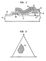
- Figure 1 shows a cross-section of a typical stacked capacitor DRAM design incorporating the dielectric layer of this invention; however, it is to be understood that the invention is not limited to use with DRAM cells, but may be used in other applications as well, such as hybrid integrated circuits or capacitors of other devices.
- the substrate 10 comprised typically of silicon, contains source 14 and drain 16 diffusions for the MOFSET, as well as MOFSET gate structures 18a, 18b.
- the substrate 10 will have disposed on its surface a field oxide pattern (or FOX) 12.
- the capacitor is disposed on the silicon substrate 10, comprising a bottom electrode 22 and top electrode 26, separated by a thin film of a dielectric material 24.
- the electrodes 22, 26 may be comprised of thin films of Ti, TiN, Al, Al doped with 0.5% Cu, or other materials known in the art for forming electrodes for DRAM applications.
- the dielectric film 24 fills the space between the bottom electrode 22 and top electrode 26, and is comprised ofZr-Sn-Ti-O or Hf-Sn-Ti-O, which also may be doped with nitrogen.
- An insulating layer 20 may separate the capacitor from the gate structures 18a, 18b.
- Figure 3 shows the current-voltage characteristics for a capacitor formed on the region of the film with the approximate composition of Zr 0.3 Sn 0.8 Ti 0.9 O 2 (within the above preferred range), plotting the current density versus electric field.
- the figure of merit for this particular capacitor was 16.9 ⁇ C/cm 2 .
- Figure 5 shows the current-voltage characteristics for a capacitor formed on the region of the film with the approximate composition of Zr 0.4 Sn 0.4 Ti 1.2 O w N v (within the preferred range illustrated in Figure 4), plotting the current density versus electric field.
- the figure of merit for this particular capacitor was 22.6 ⁇ C/cm 2 .
- Films may be prepared by either off-axis or on-axis reactive sputtering.
- An apparatus useful for depositing films via radio frequency reactive sputtering is shown in Figure 6.
- the apparatus and process will now be described with reference to depositing a composition of Zr-Ti-Sn-O, with and without doping by nitrogen, although it is understood that the same process may be employed to deposit a film of Hf-Ti-Sn-O, by using an Hf target gun in place of the Zr gun described below.
- the apparatus comprises a vacuum chamber 30, having planar magnetron sputter guns 31, 32, and 33.
- the guns 31, 32, and 33 advantageously have two-inch diameter targets and are arranged in a facing-targets configuration (i.e., toward the substrate to be coated 34), for depositing Zr, Ti, and Sn, respectively.
- the targets are disposed approximately two centimeters from opposite ends of the substrate, which typically has a rectangular shape.
- the sputter guns each are connected to an RF power source (31a, 32a, and 33a), and allowed to self-bias.
- the guns advantageously may be run at 150W (for the Zr gun 31), 75W (for the Ti gun 32), and 20W (for the Sn gun 33), to provide an appropriate Zr-Ti-Sn-O composition at a substrate midpoint.
- Depositions may be performed with a total pressure of 4.0Pa (30 mTorr) for off-axis sputtering and 0.53Pa (4.0 mTorr) for on-axis sputtering, using various flow rates, as will be further described below.
- a substrate 34 used for deposition of the thin dielectric films typically comprise silicon wafers coated with about 550 nm (5500 Angstroms) thermal oxide, 45 nm (450 Angstroms) Ti, and 60 nm (600 Angstroms) TiN.
- the substrate 34 may be mounted to a thick aluminium substrate holder (hidden from view in Fig. 6), using tantalum spring clips 35a, 35b, and 35c.
- the substrate 34 may be connected to a power source 34a, for providing RF power (preferably about 10W), during the deposition process to promote the surface mobility on the film.
- the substrate holder (not shown), may be heated using a tantalum-wire radiant heater and monitored with a chromel/alumel thermocouple inserted into the substrate holder. Preferably, the temperature should remain constant during the deposition process.
- the substrate 34 is provided, coated as previously described or with about 60 nm of TiN.
- the substrate is mounted onto the substrate holder using the Tantalum-clips 35a, 35b, and 35c, and disposed so that the substrate is about 6 centimeters from the Zr sputter gun target 31, 4 centimeters from the Ti sputter gun target 32, and 6.5 centimeters from the Sn sputter gun target 33.
- the sputter guns 31, 32, and 33 are positioned along the same horizontal plane and arranged with their targets facing inward and at 90 degree angles relative to each other, as shown in FIG. 6.
- the substrate 34 is positioned so that its top surface is disposed parallel to the horizontal plane of the targets, but disposed about 3.5 centimeters below the plane of the targets.
- the deposition process may be carried out.
- the background pressure within the vacuum chamber should be pumped to an approximate pressure of lower than 6.7 x 10 -4 Pa (5 x 10 -6 Torr).
- the temperature of the substrate 34 should be raised to about 200 degrees Centigrade, maintained within ten or twenty degrees.
- the oxygen (O 2 ) gas is then introduced, along with Argon gas, at 10 sccm and 15 sccm, respectively (wherein "sccm” refers to standard cubic centimeters per minute, i.e., at standard pressure and temperature).
- the pressure of the sputtering gas should be raised to about 4.0 Pa (30.0 mTorr).
- the RF power sources 34a, 31a, 32a, and 33a are then activated to apply RF power to the substrate 34 and sputtering guns 31, 32, and 33, at 10W, 75W, 150W, and 20W, respectively, as previously described.
- RF matching circuits may be tuned for each RF power supply 31a, 32a, 33a, and 34a, to obtain the minimum reflected power.
- the sputtered deposition should be run for about twenty minutes, and then the RF power and gas supplies turned off. The system may then be vented and the sample retrieved.
- the same process may be used, except that nitrogen gas would need to be pumped into the vacuum chamber along with the oxygen and argon gas.
- gas flow rates of about 5 sccm N 2 gas, 10 sccm O 2 gas, and 10 sccm Ar gas may advantageously be used.
- An on-axis sputtering deposition process involving one composite sputtering gun, also is advantageous and reduces the process time.
- a composite Zr-Sn-Ti metal target is used, having a composition of 60%Ti, 20% Zr, and 20% Sn (in atomic %), suitable for a two-inch diameter sputter gun.
- the substrate is mounted onto a substrate holder and held in place using Ta-clips for thermal contact.
- the substrate should be positioned about 3.0 centimeters from the composite metal target, with its surface oriented parallel with and centered with respect to the target.
- the parameters for the background pressure gas, the temperature substrate, and rate of gas flow are the same as for off-axis deposition, described above (i.e., background gas pressure is pumped to lower than 6.7 x 10 -4 Pa (5 x 10 -6 Torr); the temperature of the substrate is maintained at about 200 degrees Centigrade, and gases are introduced at 10 sccm for O 2 gas and 15 sccm for Ar gas).
- the pressure of the sputtering gas may be raised, however, to about 0.53 Pa (4.0 mTorr).
- the RF power applied to the composite sputtering gun may be about 100W, tuned with an RF matching circuit to obtain the minimum reflected power.
- the sputtered deposition can be run for five minutes, and then the RF power and gas supplies turned off. Once the substrate has cooled to about 100 degrees Centigrade, the system may then be vented and the sample retrieved.
- the hybrid integrated circuit of this invention should not be limited to the examples or method of preparation described above.
- R-Sn-Ti-O as the main component (where R is Zr or Hf)
- RF radio frequency
- other methods such as ion beam sputtering, chemical vapor deposition, electron cyclotron resonance sputtering, or laser ablation.
- the films can be doped with small concentrations of appropriate elements to compensate for oxygen traps (e.g., Mg, Ca, Sr, Y, Al, or In). All such variations and modifications are intended to be included within the scope of the appended claims.
Landscapes
- Semiconductor Memories (AREA)
- Semiconductor Integrated Circuits (AREA)
- Inorganic Insulating Materials (AREA)
- Fixed Capacitors And Capacitor Manufacturing Machines (AREA)
- Compositions Of Oxide Ceramics (AREA)
Claims (9)
- Film diélectrique pour utilisation dans un condensateur comprenant une composition amorphe de RxSnyTizOw comme composant principal, dans lequel R est choisi dans le groupe constitué du zirconium (Zr) et du hafnium (Hf), caractérisé en ce que x, y, z et w sont 0,1 ≤ x ≤ 1,8 ; 0,1 ≤ y ≤ 1,6 ; 0,2 ≤ z ≤ 1,9 ; et 2,0 ≤ w ≤ 4,0 ; et x + y + z = 2.
- Film diélectrique selon la revendication 1, dans lequel x est approximativement 0,3, y est approximativement 0,9 et z est approximativement 0,8.
- Film diélectrique selon la revendication 1, dans lequel x est approximativement 0,4, y est approximativement 0,4 et z est approximativement 1,2.
- Film diélectrique selon la revendication 1, dans lequel la composition amorphe est en outre dopée avec de l'azote.
- Film diélectrique selon la revendication 4, dans lequel la composition comprend RxSnyTizOw,Nv où v est 0,01 ≤ v ≤ 0,03.
- Film diélectrique selon la revendication 5, dans lequel x est approximativement 0,4, y est approximativement 0,4 et z est approximativement 1,2.
- Condensateur comprenant une paire d'électrodes et, disposée entre les électrodes, une couche de matériau diélectrique comprenant une composition amorphe de RxSnyTizOw comme composant principal, dans lequel R est choisi dans le groupe qui est constitué du zirconium et du hafnium, caractérisé en ce que x, y, z et w sont 0,1 ≤ x ≤ 1,8 ; 0,1 ≤ y ≤ 1,6 ; 0,2 ≤ z ≤ 1,9 ; et 2,0 ≤ w ≤ 4,0 ; et x + y + z = 2.
- Condensateur selon la revendication 7, dans lequel la composition amorphe est en outre dopée avec de l'azote.
- Condensateur selon la revendication 7, dans lequel la composition comprend RxSnyTizOw,Nv où v est 0,01 ≤ v ≤ 0,03.
Applications Claiming Priority (2)
| Application Number | Priority Date | Filing Date | Title |
|---|---|---|---|
| US936132 | 1997-09-24 | ||
| US08/936,132 US5912797A (en) | 1997-09-24 | 1997-09-24 | Dielectric materials of amorphous compositions and devices employing same |
Publications (3)
| Publication Number | Publication Date |
|---|---|
| EP0905723A2 EP0905723A2 (fr) | 1999-03-31 |
| EP0905723A3 EP0905723A3 (fr) | 1999-12-29 |
| EP0905723B1 true EP0905723B1 (fr) | 2004-08-04 |
Family
ID=25468217
Family Applications (1)
| Application Number | Title | Priority Date | Filing Date |
|---|---|---|---|
| EP98307232A Expired - Lifetime EP0905723B1 (fr) | 1997-09-24 | 1998-09-08 | Matériaux diélectriques amorphes et condensateurs utilisant ceux-ci |
Country Status (4)
| Country | Link |
|---|---|
| US (1) | US5912797A (fr) |
| EP (1) | EP0905723B1 (fr) |
| JP (1) | JP3649917B2 (fr) |
| DE (1) | DE69825384T2 (fr) |
Families Citing this family (39)
| Publication number | Priority date | Publication date | Assignee | Title |
|---|---|---|---|---|
| US6320238B1 (en) * | 1996-12-23 | 2001-11-20 | Agere Systems Guardian Corp. | Gate structure for integrated circuit fabrication |
| KR100353863B1 (ko) * | 1998-09-10 | 2003-01-24 | 주식회사 케이티 | 마이크로파유전체세라믹조성물 |
| US6265260B1 (en) | 1999-01-12 | 2001-07-24 | Lucent Technologies Inc. | Method for making an integrated circuit capacitor including tantalum pentoxide |
| GB9922572D0 (en) * | 1999-09-24 | 1999-11-24 | Koninkl Philips Electronics Nv | Capacitive sensing array devices |
| US6437392B1 (en) * | 1999-12-08 | 2002-08-20 | Agere Systems Optoelectronics Guardian Corp. | Article comprising a dielectric material of ZR-Ge-Ti-O or Hf-Ge-Ti-O and method of making the same |
| US6500499B1 (en) * | 2000-03-10 | 2002-12-31 | Air Products And Chemicals, Inc. | Deposition and annealing of multicomponent ZrSnTi and HfSnTi oxide thin films using solventless liquid mixture of precursors |
| US6495474B1 (en) | 2000-09-11 | 2002-12-17 | Agere Systems Inc. | Method of fabricating a dielectric layer |
| US6852167B2 (en) | 2001-03-01 | 2005-02-08 | Micron Technology, Inc. | Methods, systems, and apparatus for uniform chemical-vapor depositions |
| US7037862B2 (en) * | 2001-06-13 | 2006-05-02 | Micron Technology, Inc. | Dielectric layer forming method and devices formed therewith |
| US8026161B2 (en) | 2001-08-30 | 2011-09-27 | Micron Technology, Inc. | Highly reliable amorphous high-K gate oxide ZrO2 |
| US6559014B1 (en) * | 2001-10-15 | 2003-05-06 | Advanced Micro Devices, Inc. | Preparation of composite high-K / standard-K dielectrics for semiconductor devices |
| US6900122B2 (en) * | 2001-12-20 | 2005-05-31 | Micron Technology, Inc. | Low-temperature grown high-quality ultra-thin praseodymium gate dielectrics |
| US6953730B2 (en) | 2001-12-20 | 2005-10-11 | Micron Technology, Inc. | Low-temperature grown high quality ultra-thin CoTiO3 gate dielectrics |
| US7160577B2 (en) | 2002-05-02 | 2007-01-09 | Micron Technology, Inc. | Methods for atomic-layer deposition of aluminum oxides in integrated circuits |
| US7589029B2 (en) | 2002-05-02 | 2009-09-15 | Micron Technology, Inc. | Atomic layer deposition and conversion |
| US7221586B2 (en) | 2002-07-08 | 2007-05-22 | Micron Technology, Inc. | Memory utilizing oxide nanolaminates |
| US6921702B2 (en) | 2002-07-30 | 2005-07-26 | Micron Technology Inc. | Atomic layer deposited nanolaminates of HfO2/ZrO2 films as gate dielectrics |
| US6884739B2 (en) * | 2002-08-15 | 2005-04-26 | Micron Technology Inc. | Lanthanide doped TiOx dielectric films by plasma oxidation |
| US6790791B2 (en) | 2002-08-15 | 2004-09-14 | Micron Technology, Inc. | Lanthanide doped TiOx dielectric films |
| JP2004143584A (ja) * | 2002-08-29 | 2004-05-20 | Nippon Sheet Glass Co Ltd | ジルコニウム化合物膜が被覆された物品、その物品の製造方法及びその膜を被覆するために用いるスパッタリングターゲット |
| US7084078B2 (en) * | 2002-08-29 | 2006-08-01 | Micron Technology, Inc. | Atomic layer deposited lanthanide doped TiOx dielectric films |
| US7101813B2 (en) | 2002-12-04 | 2006-09-05 | Micron Technology Inc. | Atomic layer deposited Zr-Sn-Ti-O films |
| US6958302B2 (en) | 2002-12-04 | 2005-10-25 | Micron Technology, Inc. | Atomic layer deposited Zr-Sn-Ti-O films using TiI4 |
| US7192892B2 (en) | 2003-03-04 | 2007-03-20 | Micron Technology, Inc. | Atomic layer deposited dielectric layers |
| US7183186B2 (en) | 2003-04-22 | 2007-02-27 | Micro Technology, Inc. | Atomic layer deposited ZrTiO4 films |
| US20040245602A1 (en) * | 2003-05-21 | 2004-12-09 | Kim Sun Jung | Method of fabricating metal-insulator-metal capacitor (MIM) using lanthanide-doped HfO2 |
| US7192824B2 (en) | 2003-06-24 | 2007-03-20 | Micron Technology, Inc. | Lanthanide oxide / hafnium oxide dielectric layers |
| US7220665B2 (en) * | 2003-08-05 | 2007-05-22 | Micron Technology, Inc. | H2 plasma treatment |
| US7524774B2 (en) * | 2003-09-26 | 2009-04-28 | Tokyo Electron Limited | Manufacturing method of semiconductor device, semiconductor manufacturing apparatus, plasma nitridation method, computer recording medium, and program |
| KR100585114B1 (ko) * | 2003-12-05 | 2006-05-30 | 삼성전자주식회사 | 비티에스 또는 비티지 물질로 이루어진 고유전체막을구비하는 반도체 소자의 커패시터 및 그 제조방법 |
| US20050233477A1 (en) * | 2004-03-05 | 2005-10-20 | Tokyo Electron Limited | Substrate processing apparatus, substrate processing method, and program for implementing the method |
| US7588988B2 (en) | 2004-08-31 | 2009-09-15 | Micron Technology, Inc. | Method of forming apparatus having oxide films formed using atomic layer deposition |
| US7687409B2 (en) | 2005-03-29 | 2010-03-30 | Micron Technology, Inc. | Atomic layer deposited titanium silicon oxide films |
| US7662729B2 (en) | 2005-04-28 | 2010-02-16 | Micron Technology, Inc. | Atomic layer deposition of a ruthenium layer to a lanthanide oxide dielectric layer |
| US7927948B2 (en) | 2005-07-20 | 2011-04-19 | Micron Technology, Inc. | Devices with nanocrystals and methods of formation |
| US7393736B2 (en) * | 2005-08-29 | 2008-07-01 | Micron Technology, Inc. | Atomic layer deposition of Zrx Hfy Sn1-x-y O2 films as high k gate dielectrics |
| US7563730B2 (en) | 2006-08-31 | 2009-07-21 | Micron Technology, Inc. | Hafnium lanthanide oxynitride films |
| US9224878B2 (en) * | 2012-12-27 | 2015-12-29 | Intermolecular, Inc. | High work function, manufacturable top electrode |
| US12588438B2 (en) | 2021-11-25 | 2026-03-24 | Samsung Electronics Co., Ltd. | Layer structures including dielectric layer, methods of manufacturing dielectric layer, electronic device including dielectric layer, and electronic apparatus including electronic device |
Family Cites Families (2)
| Publication number | Priority date | Publication date | Assignee | Title |
|---|---|---|---|---|
| JPH06334140A (ja) * | 1992-12-16 | 1994-12-02 | Ricoh Co Ltd | 強誘電体材料および該材料を用いた半導体メモリ、光記録媒体ならびに微小変位制御素子 |
| US5644184A (en) * | 1996-02-15 | 1997-07-01 | Thermodyne, Inc. | Piezo-pyroelectric energy converter and method |
-
1997
- 1997-09-24 US US08/936,132 patent/US5912797A/en not_active Expired - Lifetime
-
1998
- 1998-09-08 EP EP98307232A patent/EP0905723B1/fr not_active Expired - Lifetime
- 1998-09-08 DE DE69825384T patent/DE69825384T2/de not_active Expired - Lifetime
- 1998-09-22 JP JP26877598A patent/JP3649917B2/ja not_active Expired - Fee Related
Also Published As
| Publication number | Publication date |
|---|---|
| JPH11168027A (ja) | 1999-06-22 |
| DE69825384T2 (de) | 2005-09-08 |
| JP3649917B2 (ja) | 2005-05-18 |
| DE69825384D1 (de) | 2004-09-09 |
| US5912797A (en) | 1999-06-15 |
| EP0905723A2 (fr) | 1999-03-31 |
| EP0905723A3 (fr) | 1999-12-29 |
Similar Documents
| Publication | Publication Date | Title |
|---|---|---|
| EP0905723B1 (fr) | Matériaux diélectriques amorphes et condensateurs utilisant ceux-ci | |
| US6093944A (en) | Dielectric materials of amorphous compositions of TI-O2 doped with rare earth elements and devices employing same | |
| US5977582A (en) | Capacitor comprising improved TaOx -based dielectric | |
| US5973911A (en) | Ferroelectric thin-film capacitor | |
| US5663088A (en) | Method of forming a Ta2 O5 dielectric layer with amorphous diffusion barrier layer and method of forming a capacitor having a Ta2 O5 dielectric layer and amorphous diffusion barrier layer | |
| JP2012041633A (ja) | Zr−Ge−Ti−OまたはHf−Ge−Ti−Oの誘電材料を備えた物質とその製造方法 | |
| JPH026205B2 (fr) | ||
| Lin et al. | The temperature dependence of the conduction current in Ba 0.5 Sr 0.5 TiO 3 thin-film capacitors for memory device applications | |
| US5874379A (en) | Dielectric thin film and fabrication method thereof | |
| Peng et al. | Electrical properties of strontium titanate thin films by multi‐ion‐beam reactive sputtering technique | |
| US5985757A (en) | Method for fabricating semiconductor device | |
| KR100321561B1 (ko) | 휘발 성분이 포함된 다성분 산화물 강유전체 박막의 제조방법 | |
| Li et al. | Reactive partially ionized beam deposition of BaTiO3 thin films | |
| US5820946A (en) | Method for fabricating ferroelectric thin film | |
| JP3108797B2 (ja) | 高誘電率誘電体薄膜の製造方法 | |
| JP3427362B2 (ja) | 誘電体薄膜堆積方法 | |
| EP0631332B1 (fr) | Procédé de fabrication d'une couche mince supraconductrice en Y-Ba-Cu-O | |
| KR100315885B1 (ko) | 전자부품에서사용하기위한유전체박막형성방법 | |
| KR100265846B1 (ko) | 반도체소자의강유전체캐패시터제조방법 | |
| Krupanidhi et al. | Effect of low pressure dc plasma discharge on laser ablated ferroelectric Pb (Zr, Ti) O3 thin films | |
| Peng et al. | Low‐energy oxygen ion bombardment effect on BaTiO3 thin films grown by multi‐ion‐beam reactive sputtering technique | |
| JPH06140570A (ja) | 高誘電率誘電体薄膜を有する電子部品とその製造方法 | |
| US20040245602A1 (en) | Method of fabricating metal-insulator-metal capacitor (MIM) using lanthanide-doped HfO2 | |
| US6391797B1 (en) | Method of manufacturing semiconductor device by sputtering dielectric forming materials while selectively heating growing layer | |
| Yamakawa et al. | Development of stable PZT sputtering process using ex-situ crystallization and PZT/Pt interface control technique |
Legal Events
| Date | Code | Title | Description |
|---|---|---|---|
| PUAI | Public reference made under article 153(3) epc to a published international application that has entered the european phase |
Free format text: ORIGINAL CODE: 0009012 |
|
| AK | Designated contracting states |
Kind code of ref document: A2 Designated state(s): DE FR GB |
|
| AX | Request for extension of the european patent |
Free format text: AL;LT;LV;MK;RO;SI |
|
| PUAL | Search report despatched |
Free format text: ORIGINAL CODE: 0009013 |
|
| AK | Designated contracting states |
Kind code of ref document: A3 Designated state(s): AT BE CH CY DE DK ES FI FR GB GR IE IT LI LU MC NL PT SE |
|
| AX | Request for extension of the european patent |
Free format text: AL;LT;LV;MK;RO;SI |
|
| 17P | Request for examination filed |
Effective date: 20000615 |
|
| AKX | Designation fees paid |
Free format text: DE FR GB |
|
| 17Q | First examination report despatched |
Effective date: 20011113 |
|
| GRAP | Despatch of communication of intention to grant a patent |
Free format text: ORIGINAL CODE: EPIDOSNIGR1 |
|
| GRAS | Grant fee paid |
Free format text: ORIGINAL CODE: EPIDOSNIGR3 |
|
| GRAA | (expected) grant |
Free format text: ORIGINAL CODE: 0009210 |
|
| AK | Designated contracting states |
Kind code of ref document: B1 Designated state(s): DE FR GB |
|
| REG | Reference to a national code |
Ref country code: GB Ref legal event code: FG4D |
|
| REF | Corresponds to: |
Ref document number: 69825384 Country of ref document: DE Date of ref document: 20040909 Kind code of ref document: P |
|
| ET | Fr: translation filed | ||
| PLBE | No opposition filed within time limit |
Free format text: ORIGINAL CODE: 0009261 |
|
| STAA | Information on the status of an ep patent application or granted ep patent |
Free format text: STATUS: NO OPPOSITION FILED WITHIN TIME LIMIT |
|
| 26N | No opposition filed |
Effective date: 20050506 |
|
| PGFP | Annual fee paid to national office [announced via postgrant information from national office to epo] |
Ref country code: FR Payment date: 20140906 Year of fee payment: 17 |
|
| REG | Reference to a national code |
Ref country code: DE Ref legal event code: R082 Ref document number: 69825384 Country of ref document: DE Representative=s name: DILG HAEUSLER SCHINDELMANN PATENTANWALTSGESELL, DE |
|
| PGFP | Annual fee paid to national office [announced via postgrant information from national office to epo] |
Ref country code: GB Payment date: 20150825 Year of fee payment: 18 |
|
| REG | Reference to a national code |
Ref country code: FR Ref legal event code: ST Effective date: 20160531 |
|
| PG25 | Lapsed in a contracting state [announced via postgrant information from national office to epo] |
Ref country code: FR Free format text: LAPSE BECAUSE OF NON-PAYMENT OF DUE FEES Effective date: 20150930 |
|
| PGFP | Annual fee paid to national office [announced via postgrant information from national office to epo] |
Ref country code: DE Payment date: 20160823 Year of fee payment: 19 |
|
| GBPC | Gb: european patent ceased through non-payment of renewal fee |
Effective date: 20160908 |
|
| PG25 | Lapsed in a contracting state [announced via postgrant information from national office to epo] |
Ref country code: GB Free format text: LAPSE BECAUSE OF NON-PAYMENT OF DUE FEES Effective date: 20160908 |
|
| REG | Reference to a national code |
Ref country code: DE Ref legal event code: R119 Ref document number: 69825384 Country of ref document: DE |
|
| PG25 | Lapsed in a contracting state [announced via postgrant information from national office to epo] |
Ref country code: DE Free format text: LAPSE BECAUSE OF NON-PAYMENT OF DUE FEES Effective date: 20180404 |