EP0904981A2 - Verfahren und Schaltungsanordnung zur Leuchtweitenregulierung eines Scheinwerfers - Google Patents
Verfahren und Schaltungsanordnung zur Leuchtweitenregulierung eines Scheinwerfers Download PDFInfo
- Publication number
- EP0904981A2 EP0904981A2 EP98114238A EP98114238A EP0904981A2 EP 0904981 A2 EP0904981 A2 EP 0904981A2 EP 98114238 A EP98114238 A EP 98114238A EP 98114238 A EP98114238 A EP 98114238A EP 0904981 A2 EP0904981 A2 EP 0904981A2
- Authority
- EP
- European Patent Office
- Prior art keywords
- signal
- headlight
- terminal
- transistor
- circuit arrangement
- Prior art date
- Legal status (The legal status is an assumption and is not a legal conclusion. Google has not performed a legal analysis and makes no representation as to the accuracy of the status listed.)
- Granted
Links
- 238000000034 method Methods 0.000 title claims description 14
- 239000003990 capacitor Substances 0.000 claims description 21
- 230000000873 masking effect Effects 0.000 claims description 10
- 230000001105 regulatory effect Effects 0.000 claims description 2
- 238000010586 diagram Methods 0.000 description 4
- 230000000903 blocking effect Effects 0.000 description 1
- 239000000919 ceramic Substances 0.000 description 1
- 239000003985 ceramic capacitor Substances 0.000 description 1
- 238000006243 chemical reaction Methods 0.000 description 1
- 230000008878 coupling Effects 0.000 description 1
- 238000010168 coupling process Methods 0.000 description 1
- 238000005859 coupling reaction Methods 0.000 description 1
- 230000001419 dependent effect Effects 0.000 description 1
- 238000011161 development Methods 0.000 description 1
- 230000018109 developmental process Effects 0.000 description 1
- 230000000694 effects Effects 0.000 description 1
- 238000013021 overheating Methods 0.000 description 1
- 238000005096 rolling process Methods 0.000 description 1
- 239000004065 semiconductor Substances 0.000 description 1
Images

Classifications
-
- B—PERFORMING OPERATIONS; TRANSPORTING
- B60—VEHICLES IN GENERAL
- B60Q—ARRANGEMENT OF SIGNALLING OR LIGHTING DEVICES, THE MOUNTING OR SUPPORTING THEREOF OR CIRCUITS THEREFOR, FOR VEHICLES IN GENERAL
- B60Q1/00—Arrangement of optical signalling or lighting devices, the mounting or supporting thereof or circuits therefor
- B60Q1/02—Arrangement of optical signalling or lighting devices, the mounting or supporting thereof or circuits therefor the devices being primarily intended to illuminate the way ahead or to illuminate other areas of way or environments
- B60Q1/04—Arrangement of optical signalling or lighting devices, the mounting or supporting thereof or circuits therefor the devices being primarily intended to illuminate the way ahead or to illuminate other areas of way or environments the devices being headlights
- B60Q1/06—Arrangement of optical signalling or lighting devices, the mounting or supporting thereof or circuits therefor the devices being primarily intended to illuminate the way ahead or to illuminate other areas of way or environments the devices being headlights adjustable, e.g. remotely-controlled from inside vehicle
- B60Q1/08—Arrangement of optical signalling or lighting devices, the mounting or supporting thereof or circuits therefor the devices being primarily intended to illuminate the way ahead or to illuminate other areas of way or environments the devices being headlights adjustable, e.g. remotely-controlled from inside vehicle automatically
- B60Q1/10—Arrangement of optical signalling or lighting devices, the mounting or supporting thereof or circuits therefor the devices being primarily intended to illuminate the way ahead or to illuminate other areas of way or environments the devices being headlights adjustable, e.g. remotely-controlled from inside vehicle automatically due to vehicle inclination, e.g. due to load distribution
- B60Q1/115—Arrangement of optical signalling or lighting devices, the mounting or supporting thereof or circuits therefor the devices being primarily intended to illuminate the way ahead or to illuminate other areas of way or environments the devices being headlights adjustable, e.g. remotely-controlled from inside vehicle automatically due to vehicle inclination, e.g. due to load distribution by electric means
Definitions
- the invention relates to a method for headlight range control a headlamp according to the preamble of the claim 1 and a circuit arrangement according to the preamble of Claim 7.
- a Headlight range control is therefore necessary so that the Headlights adjusted depending on the load of the vehicle are that oncoming traffic is not dazzled.
- motor vehicles are either continuous headlamp levelers or switchable headlamp leveling is common.
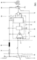
- a known circuit arrangement for headlight range control of a motor vehicle headlight shows Figure 5.
- the circuit is structured as follows.
- a setpoint generator 14 is connected in the form of a transmitter potentiometer.
- This setpoint generator 14 is located in the area of the dashboard A of the motor vehicle.
- the center tap of the setpoint generator 14 and the supply voltage terminal 1 are connected to a headlamp leveling device C mechanically coupled to the headlight 10 via suitable feed lines B.
- the supply lines B are represented in an equivalent circuit by the series connection of a resistor 16 with a downstream coil 18.
- the headlamp leveling device C has a drive motor 12 for adjusting the height and / or inclination of the headlight 10. The adjustment is indicated schematically by the arrow P.
- An actual value transmitter 28, here a so-called feedback potentiometer, is coupled to the headlight 10, between its center tap and the reference potential terminal 3 a signal V FB, which is representative of the current position of the headlight 10, can be grasped.
- the headlight range adjuster C has a control device IC with an input-side comparison stage 20 and an output-side driver stage 24, to which the drive motor 12 is connected.
- a logic unit 22 is connected between the comparison stage 20, which is regularly subject to hysteresis, and the driver stage 24. To supply voltage to the comparison stage 20, the logic unit 22 and the driver stage 24, these are connected with leads to the supply voltage V S provided via the series connection of the resistor 16 and the coil 18 and to reference potential.
- An electrolytic capacitor which will be explained in more detail, is connected between the reference potential terminal 3 and the line for the supply voltage V S.
- the comparison stage 20 is connected with its one input terminal to the center tap of the setpoint generator 14 and receives a setpoint signal V 14 from there. At the other input terminal, the comparison stage 20 receives the actual signal V FB and forms a differential voltage ⁇ V at its output, which is subject to hysteresis.
- the setpoint device on the dashboard A enables the driver of the motor vehicle to individually adjust the headlight position. Due to the necessary mechanical coupling of the motor 12 and the actual value transmitter 28 with the headlight 10, the headlight range adjuster C is accommodated directly on the headlight 10.
- the drive motor 12 is driven by the driver stage 24, which is preferably a full-bridge circuit. Depending on the position of the setpoint generator 14, the headlamp 10 is to be more or less faded in or out, that is to say its inclination angle is adjusted.
- the actual value transmitter 28 is used as an angle sensor. This delivers the actual signal V FB and is mechanical with the drive motor 12 and z. B. connected via a worm drive with the pitching mechanism of the headlight 10.
- the signal V 14 supplied from the reference value generator 14 is compared in the comparator 20 with the signal V FB. Depending on the differential voltage V, the drive motor 12 rotates and changes the signal V FB until the differential signal ⁇ V becomes zero.
- the invention has the aim of a method and a circuit arrangement for headlight range adjustment indicate the use of an electrolytic capacitor with high capacity makes it unnecessary and therefore small to be built.
- the invention essentially sees an additional device before, the result of a Actual / target comparison of the control loop for a given one Time blocked and thus hidden.
- the output signal the comparison level remains within the control device for this time without effect.
- the circuit arrangement shown in Fig. 1 corresponds to to the differences in the circuit arrangement explained below of Fig. 5.
- the crucial difference to 5 consists in the circuit arrangement 1 in that in the control device IC, which is preferably designed as an integrated circuit, a fade-out device 30 which is connected to the logic unit 22 is coupled in a manner yet to be explained.
- the blanking device 30 receives a signal from logic unit 22 START, processes this signal and directs the logic unit 22 a signal BLANK.
- the masking device 30 is via a capacitor 40 which is outside the control device IC is arranged, connected to reference potential.
- the capacitor 26 now not as an electrolytic capacitor, but as Capacitor formed with a relatively low capacitance is.
- the capacitor 26 also serves as a filter capacitor, can be reduced to some 100 nF, however. So that is the use of an inexpensive, small temperature-resistant SMD-capable (surface mounted device) and reliable ceramic Capacity possible.
- the masking device 30 ensures that the output signal the comparison stage 20 for a predetermined period of time remains ineffective and is therefore hidden.
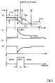
- the main voltage and current profiles are shown in FIG. 2 for a better understanding of this function. This will be discussed further below.
- the fade-out time can be individually adapted to the respective application with a ceramic capacitor of relatively low capacitance (cf. FIG. 3).
- the capacitor 26 is still required to limit the voltage change rate (dV S / dt). Too high a rate of voltage change (“slew rate”) has repercussions from the driver stage 24 on the logic unit 22 and the comparison stage 20. Such reactions occur particularly when the control device IC is monolithically integrated in a semiconductor body.
- FIG. 2 four time diagrams of voltage and current profiles are shown with respect to one another.
- the uppermost curve shows the voltage signal V 14 , which, starting from a higher value at time a, is gradually reduced to a lower value by corresponding actuation of the setpoint generator 14 (cf. FIG. 1). This lower value is reached at time c.
- V HY denotes the hysteresis voltage of comparison stage 20.
- signal V 14 reaches the lower hysteresis value of comparison stage 20.
- drive motor 12 starts.
- Motor current I M jumps to high blocking current I STALL at time b and then to drop to the nominal current I NENN with the mechanical time constant.
- V S drops abruptly at time b.
- the actual value signal V FB breaks in accordance with the dashed line in the upper signal diagram at time b and drops significantly below the desired signal V 14 .
- the drive motor 12 would be stopped in this case and controlled in reverse since V FB ⁇ (V 14 -1/2 V HY ) is.
- the masking device 30 ensures that the output signal of the comparison stage 20 is suppressed for a predetermined period of time immediately after the start of the drive motor 12, ie at time b.
- the predetermined period of time is selected such that V FB > V 14 is in any case after the period of time has elapsed.
- the fade-out time t A is chosen to be so long that its end is somewhat after the time c.
- the signal V FB jumps suddenly below V 14 at the time b and then gradually rises again. After the blanking time t A , the signal V FB drops until the time d at which the drive motor 12 is switched off.
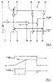
- FIG. 3 shows an exemplary embodiment of the masking device 30 from FIG. 1.
- the circuit has the capacitor 40 already explained, which can have, for example, a capacitance value of 47 nF and is connected with one connection to the reference potential terminal 3 and with its other connection to a terminal of the control device.
- This terminal is designated by the reference symbol K and, within the masking device 30, is connected to the non-inverting input of a comparator 38.
- the inverting input of the comparator 38 is in contact with a reference voltage V REF .
- the terminal K is also connected via a current source 31 to the supply voltage terminal 5 for the supply voltage V S.
- Terminal K is additionally connected to reference potential terminal 3 via the load path of a bipolar transistor 32.
- the output terminal of the comparator 38 is connected to the control terminal of a second transistor 34.
- the load path of this second transistor 34 lies between the reference potential terminal 3 and a terminal at which the BLANK signal can be tapped.
- This terminal is connected to the supply voltage terminal 5 via a resistor 37.
- this terminal is connected to the reference potential terminal 3 via the load path of a third transistor 35.
- the control connection of this third transistor 35 is connected to the control connection of the first transistor 32 and is connected to the reference potential terminal 3 via the load path of a fourth transistor 33.
- the connection point of the two control connections of the transistors 32, 35 is also connected to the supply voltage terminal 5 via a resistor 36.
- the control connection of the fourth transistor is connected to a terminal for the START signal.
- the resistors 36, 37 mentioned can also be replaced by current sources.
- this masking device 30 becomes clear in connection with the signal profiles of FIG. 4. If the difference V 14 - V FB (cf. FIG. 1) is greater than the switching hysteresis of the comparison stage 20, the signal START is generated, which clamps the bases of the transistors 32 and 35 via the transistor 33. As a result, the charging process of the capacitor 40 is started, as a result of which the voltage V 40 dropping across it increases. With the start of the START signal, the BLANK signal also begins at time t 0 . If the voltage V 40 reaches the reference voltage V ref , the signal BLANK is set to a low "low" level again by the transistor 34. The time period t 1 -t 0 is the blanking time t A.
- the logic unit 22 of the control device IC ensures that the output signal of the comparison stage 20 is masked out. If the signal V 14 becomes equal to the signal V FB , which is the case at time t 2 , the signal START is reset and the capacitor 40 is discharged via the transistor 32.
Landscapes
- Engineering & Computer Science (AREA)
- Mechanical Engineering (AREA)
- Lighting Device Outwards From Vehicle And Optical Signal (AREA)
Abstract
Description
- Fig. 1
- das Blockschaltbild eines Ausführungsbeispieles einer Schaltungsanordnung zur Leuchtweitenregulierung eines Scheinwerfers gemäß vorliegender Erfindung,
- Fig. 2
- die wesentlichen Spannungs- und Stromverläufe in der Schaltungsanordnung von Fig. 1,
- Fig. 3
- ein Ausführungsbeispiel für eine in der Steuereinrichtung von Fig. 1 eingesetzte Ausblendeinrichtung,
- Fig. 4
- Signalverläufe zu der Schaltungsanordnung von Fig. 3, und
- Fig. 5
- die bereits erläuterte Schaltungsanordnung zur Leuchtweitenregulierung eines Scheinwerfers nach dem Stand der Technik.
Claims (15)
- Verfahren zur Leuchtweitenregulierung eines Scheinwerfers (10), bei welchem in Abhängigkeit von aus einem Ist-/Soll-Vergleich gewonnenen Stellsignal ein mit dem Scheinwerfer (10) mechanisch gekoppelter Antriebsmotor (12) zur Verstellung des Scheinwerfers (10) angetrieben wird,
dadurch gekennzeichnet, daß nach jedem Start des Antriebsmotors (12) das Ergebnis des Ist-/Soll-Vergleiches für eine vorgegebene Zeitspanne (tA) ignoriert und damit ausgeblendet wird. - Verfahren nach Anspruch 1,
dadurch gekennzeichnet, daß das Stellsignal als Differenzsignal eines von einer manuell zu betätigenden Verstelleinrichtung (14) kommenden Soll-Signales (V14) und einem die augenblickliche Stellung des Scheinwerfers (10) entsprechenden Ist-Signales (VFB) abgeleitet wird. - Verfahren nach Anspruch 1 oder 2,
dadurch gekennzeichnet, daß das Stellsignal hysteresebehaftet ist. - Verfahren nach einem der Ansprüche 1 bis 3,
dadurch gekennzeichnet, daß die vorgegebene Zeitspanne (tA) einstellbar ist. - Verfahren nach einem der Ansprüche 1 bis 4,
dadurch gekennzeichnet, daß der Beginn (t0) der Zeitspanne (tA) durch eine vorgegebene Größe des Differenzsignales bestimmt ist und das Ende (t1) der Zeitspanne (tA) dann erreicht ist, wenn ein Kondensator (40) auf eine vorgegebene Referenzspannung (Vref) aufgeladen worden ist. - Verfahren nach Anspruch 5,
dadurch gekennzeichnet, daß ein Rücksetzsignal für einen neuen Beginn (t0) der Zeitspanne (tA) erzeugt wird, wenn das Differenzsignal mindestens annähernd gleich oder gleich 0 ist. - Schaltungsanordnung zur Leuchtweitenregulierung eines Scheinwerfers (10) mit folgenden Merkmalen:einen Antriebsmotor (12) zur Verstellung des Scheinwerfers (10);einen mit dem Scheinwerfer (10) gekoppelten Istwertgeber (28) zur Bildung eines für die augenblickliche Stellung des Scheinwerfers (10) maßgebenden Ist-Signales (VFB);einen Sollwertgeber (14) zur Bildung eines für eine Sollstellung des Scheinwerfers (10) maßgebenden Soll-Signales (V14);eine Steuereinrichtung (IC), durch welche nach Maßgabe eines aus dem Soll-Signal (V14) und dem Ist-Signal (VFB) gebildeten Differenzsignales der Antriebsmotors (12) antreibbar ist,
gekennzeichnet durch das weitere Merkmal:eine in der Steuereinrichtung (IC) vorgesehene Ausblendeinrichtung (30), durch welche nach jedem Start des Antriebsmotors (12) das Differenzsignal für eine vorgegebene Zeitspanne (tA) ausblendbar ist. - Schaltungsanordnung nach Anspruch 7,
dadurch gekennzeichnet, daß die Steuereinrichtung (IC) eingangsseitig eine Vergleichsstufe (20) und ausgangsseitig eine Treiberstufe (24) sowie eine zwischen die Vergleichsstufe (20) und die Treiberstufe (24) geschaltete Logikeinheit (22) aufweist. - Schaltungsanordnung nach Anspruch 7 oder 8,
dadurch gekennzeichnet, daß der Istwertgeber (14) und/oder der Sollwertgeber (28) durch Potentiometer gebildet ist, wobei der Mittelabgriff oder die Mittelabgriffe des oder der Potentiometer mit der Vergleichsstufe (20) der Steuereinrichtung (IC) gekoppelt ist. - Schaltungsanordnung nach einem der Ansprüche 7 bis 9,
dadurch gekennzeichnet, daß die Ausblendeinrichtung (30) einen für die Zeitspanne (tA) maßgebenden Kondensator (40) und einen Vergleicher (38) aufweist, und daß der Vergleicher (38) eingangsseitig einerseits mit einer Referenzspannung (Vref) beaufschlagbar und andererseits an den Kondensator (40) angeschlossen ist. - Schaltungsanordnung nach einem der Ansprüche 7 bis 10,
dadurch gekennzeichnet, daß die Ausblendeinrichtung (30) die Serienschaltung einer zwischen eine Versorgungsspannungsklemme (1) und Bezugspotentialklemme (3) geschalteten Reihenschaltung einer Stromquelle (31) und der Laststrecke eines Transistors (32) aufweist, daß der Kondensator (40) zwischen die Bezugspotentialklemme (3) und den Mittenabgriff der Reihenschaltung der Stromquelle (31) und des Transistors (32) geschaltet, daß der Mittenabgriff mit einer ersten Eingangsquelle des Vergleichers (38) verbunden ist, daß eine andere Eingangsklemme des Vergleichers (38) an die Referenzspannung (Vref) ankoppelbar ist, daß der Ausgang des Vergleichers (38) mit dem Steueranschluß eines zweiten Transistors (34) verbunden ist, daß die Laststrecke dieses zweiten Transistors (34) zwischen der Bezugspotentialklemme (3) und einer Ausgangsklemme für ein Ausgangssignal (BLANK) der Ausblendeinrichtung (30) verbunden ist, daß diese Ausgangsklemme über einen Widerstand (37) mit der Versorgungsspannungsklemme (1) und über die Laststrecke eines dritten Transistors (35) mit der Bezugspotentialklemme (3) in Verbindung steht, daß der Steueranschluß dieses dritten Transistors (35) mit dem Steueranschluß des ersten Transistors (32) verbunden ist und über die Laststrecke eines vierten Transistors (33) an die Bezugspotentialklemme (3) und über einen weiteren Widerstand (36) an die Versorgungsspannungsklemme (1) geschaltet ist, und daß der Steueranschluß des vierten Transistors (33) mit einer Eingangsklemme für ein Eingangssignal (START) der Ausblendeinrichtung (30) in Verbindung steht. - Schaltungsanordnung nach Anspruch 11,
dadurch gekennzeichnet, daß mindestens einer der Widerstände (36, 37) durch Stromquellen realisiert ist. - Schaltungsanordnung nach einem der Ansprüche 7 bis 12,
dadurch gekennzeichnet, daß die Steuereinrichtung (IC) als integrierter Schaltkreis ausgebildet ist. - Schaltungsanordnung nach einem der Ansprüche 7 bis 13,
dadurch gekennzeichnet, daß die Vergleichsstufe (20) eine Schalthysterese aufweist. - Schaltungsanordnung nach einem der Ansprüche 7 bis 14,
dadurch gekennzeichnet, daß der Scheinwerfer (10) ein Kfz-Scheinwerfer ist.
Applications Claiming Priority (2)
| Application Number | Priority Date | Filing Date | Title |
|---|---|---|---|
| DE19743260 | 1997-09-30 | ||
| DE1997143260 DE19743260C2 (de) | 1997-09-30 | 1997-09-30 | Verfahren und Schaltungsanordnung zur Leuchtweitenregulierung eines Scheinwerfers |
Publications (3)
| Publication Number | Publication Date |
|---|---|
| EP0904981A2 true EP0904981A2 (de) | 1999-03-31 |
| EP0904981A3 EP0904981A3 (de) | 2003-04-16 |
| EP0904981B1 EP0904981B1 (de) | 2007-12-12 |
Family
ID=7844190
Family Applications (1)
| Application Number | Title | Priority Date | Filing Date |
|---|---|---|---|
| EP19980114238 Expired - Lifetime EP0904981B1 (de) | 1997-09-30 | 1998-07-28 | Verfahren und Schaltungsanordnung zur Leuchtweitenregulierung eines Scheinwerfers |
Country Status (2)
| Country | Link |
|---|---|
| EP (1) | EP0904981B1 (de) |
| DE (2) | DE19743260C2 (de) |
Families Citing this family (1)
| Publication number | Priority date | Publication date | Assignee | Title |
|---|---|---|---|---|
| JP2001322484A (ja) * | 2000-05-12 | 2001-11-20 | Koito Mfg Co Ltd | 車輌用灯具の光軸調整装置用モータ制御回路 |
Family Cites Families (4)
| Publication number | Priority date | Publication date | Assignee | Title |
|---|---|---|---|---|
| FR2190265A5 (de) * | 1972-06-23 | 1974-01-25 | Jaeger | |
| DE2846602A1 (de) * | 1978-10-26 | 1980-05-08 | Bosch Gmbh Robert | Einrichtung fuer die selbsttaetige berichtigung der scheinwerferneigung von fahrzeugen |
| DE3827983C1 (de) * | 1988-08-18 | 1990-02-01 | Hella Kg Hueck & Co, 4780 Lippstadt, De | |
| DE4024915A1 (de) * | 1990-08-06 | 1992-02-13 | Hella Kg Hueck & Co | Verfahren und einrichtung zur regelung der leuchtweite eines kraftfahrzeugs |
-
1997
- 1997-09-30 DE DE1997143260 patent/DE19743260C2/de not_active Expired - Fee Related
-
1998
- 1998-07-28 DE DE59814136T patent/DE59814136D1/de not_active Expired - Lifetime
- 1998-07-28 EP EP19980114238 patent/EP0904981B1/de not_active Expired - Lifetime
Non-Patent Citations (1)
| Title |
|---|
| None |
Also Published As
| Publication number | Publication date |
|---|---|
| EP0904981B1 (de) | 2007-12-12 |
| DE19743260C2 (de) | 1999-10-21 |
| DE19743260A1 (de) | 1999-04-08 |
| EP0904981A3 (de) | 2003-04-16 |
| DE59814136D1 (de) | 2008-01-24 |
Similar Documents
| Publication | Publication Date | Title |
|---|---|---|
| DE60015052T2 (de) | Halbleiter-Leistungswandlungsvorrichtung | |
| EP0543826B1 (de) | Verfahren und einrichtung zur ansteuerung eines elektromagnetischen verbrauchers | |
| DE3507130A1 (de) | Treiberstromkreis fuer eine magnetspule | |
| DE3233536A1 (de) | Einrichtung zum getakteten regeln eines eine spule durchfliessenden stromes | |
| EP0671812A2 (de) | Schaltungsanordnung zur Drehzahlregelung von Elektromotoren | |
| DE102004026250B4 (de) | Ansteuerschaltung für Piezoaktoren | |
| DE10057439A1 (de) | Spannungsregler für eine gepulste Last, insbesondere für einen Mobiltelefon- oder Telematik-Sender | |
| EP0904981B1 (de) | Verfahren und Schaltungsanordnung zur Leuchtweitenregulierung eines Scheinwerfers | |
| DE69108187T2 (de) | Regelvorrichtung für die von einem Wechselstromgenerator abgegebene Batteriespannung. | |
| EP0545111A2 (de) | Einrichtung zum Verstellen der Neigung von Scheinwerfern bei Kraftfahrzeugen | |
| EP0698794A1 (de) | Schaltungsanordnung zur Unterspannungs-Erkennung | |
| WO2005083251A1 (de) | Verfahren und vorrichtung zum ansteuern eines kapazitiven stellglieds | |
| EP0098460B1 (de) | Regelvorrichtung für ein elektrisches Stellglied | |
| EP1504317B1 (de) | Spannungsversorgungsschaltung | |
| WO2006119751A2 (de) | VERFAHREN UND EINRICHTUNG ZUR ELEKTRISCHEN ANSTEUERUNG EINES VENTILS MIT EINEM MECHANISCHEN SCHLIEßELEMENT | |
| DE2826365A1 (de) | Steuereinrichtung fuer ein magnetventil | |
| EP1078460A1 (de) | Verfahren und vorrichtung zum umschalten eines feldeffekttransistors | |
| EP1326338B1 (de) | Vorrichtung zur Ansteuerung eines elektrischen Leistungsbauelements | |
| DE102007027516B4 (de) | Verfahren zur Lageveränderung mindestens eines Teils einer Beleuchtungseinrichtung für Kraftfahrzeuge | |
| DE10202279A1 (de) | Steuerschaltung für einen Aktor | |
| DE3335200A1 (de) | Spannungsversorgungseinrichtung fuer kraftfahrzeuge | |
| EP1625663A2 (de) | Integrierte schaltungsanordnung und verfahren zur programmierung einer integrierten schaltungsanordnung | |
| DE68914218T2 (de) | Spannungskommutierungsregler mit stabiliziertes Gewinn. | |
| DE102004054109A1 (de) | Vorrichtung zur Ansteuerung eines kapazitiven Lastelements | |
| DE4215034C2 (de) | Zündvorrichtung für einen Verbrennungsmotor |
Legal Events
| Date | Code | Title | Description |
|---|---|---|---|
| PUAI | Public reference made under article 153(3) epc to a published international application that has entered the european phase |
Free format text: ORIGINAL CODE: 0009012 |
|
| AK | Designated contracting states |
Kind code of ref document: A2 Designated state(s): AT BE CH CY DE DK ES FI FR GB GR IE IT LI LU MC NL PT SE |
|
| AX | Request for extension of the european patent |
Free format text: AL;LT;LV;MK;RO;SI |
|
| RAP1 | Party data changed (applicant data changed or rights of an application transferred) |
Owner name: INFINEON TECHNOLOGIES AG |
|
| PUAL | Search report despatched |
Free format text: ORIGINAL CODE: 0009013 |
|
| AK | Designated contracting states |
Designated state(s): AT BE CH CY DE DK ES FI FR GB GR IE IT LI LU MC NL PT SE |
|
| AX | Request for extension of the european patent |
Extension state: AL LT LV MK RO SI |
|
| RIC1 | Information provided on ipc code assigned before grant |
Ipc: 7B 60Q 1/076 A |
|
| 17P | Request for examination filed |
Effective date: 20030625 |
|
| AKX | Designation fees paid |
Designated state(s): DE FR GB IE IT |
|
| GRAP | Despatch of communication of intention to grant a patent |
Free format text: ORIGINAL CODE: EPIDOSNIGR1 |
|
| GRAS | Grant fee paid |
Free format text: ORIGINAL CODE: EPIDOSNIGR3 |
|
| GRAA | (expected) grant |
Free format text: ORIGINAL CODE: 0009210 |
|
| AK | Designated contracting states |
Kind code of ref document: B1 Designated state(s): DE FR GB IE IT |
|
| REG | Reference to a national code |
Ref country code: GB Ref legal event code: FG4D Free format text: NOT ENGLISH |
|
| REG | Reference to a national code |
Ref country code: IE Ref legal event code: FG4D Free format text: LANGUAGE OF EP DOCUMENT: GERMAN |
|
| REF | Corresponds to: |
Ref document number: 59814136 Country of ref document: DE Date of ref document: 20080124 Kind code of ref document: P |
|
| GBT | Gb: translation of ep patent filed (gb section 77(6)(a)/1977) |
Effective date: 20080227 |
|
| ET | Fr: translation filed | ||
| PLBE | No opposition filed within time limit |
Free format text: ORIGINAL CODE: 0009261 |
|
| STAA | Information on the status of an ep patent application or granted ep patent |
Free format text: STATUS: NO OPPOSITION FILED WITHIN TIME LIMIT |
|
| 26N | No opposition filed |
Effective date: 20080915 |
|
| REG | Reference to a national code |
Ref country code: FR Ref legal event code: PLFP Year of fee payment: 19 |
|
| PGFP | Annual fee paid to national office [announced via postgrant information from national office to epo] |
Ref country code: DE Payment date: 20160920 Year of fee payment: 19 |
|
| REG | Reference to a national code |
Ref country code: FR Ref legal event code: PLFP Year of fee payment: 20 |
|
| PGFP | Annual fee paid to national office [announced via postgrant information from national office to epo] |
Ref country code: IT Payment date: 20170728 Year of fee payment: 20 Ref country code: GB Payment date: 20170719 Year of fee payment: 20 Ref country code: FR Payment date: 20170724 Year of fee payment: 20 |
|
| PGFP | Annual fee paid to national office [announced via postgrant information from national office to epo] |
Ref country code: IE Payment date: 20170727 Year of fee payment: 20 |
|
| REG | Reference to a national code |
Ref country code: DE Ref legal event code: R119 Ref document number: 59814136 Country of ref document: DE |
|
| PG25 | Lapsed in a contracting state [announced via postgrant information from national office to epo] |
Ref country code: DE Free format text: LAPSE BECAUSE OF NON-PAYMENT OF DUE FEES Effective date: 20180201 |
|
| REG | Reference to a national code |
Ref country code: GB Ref legal event code: PE20 Expiry date: 20180727 Ref country code: IE Ref legal event code: MK9A |
|
| PG25 | Lapsed in a contracting state [announced via postgrant information from national office to epo] |
Ref country code: IE Free format text: LAPSE BECAUSE OF EXPIRATION OF PROTECTION Effective date: 20180728 |
|
| PG25 | Lapsed in a contracting state [announced via postgrant information from national office to epo] |
Ref country code: GB Free format text: LAPSE BECAUSE OF EXPIRATION OF PROTECTION Effective date: 20180727 |