EP0904981A2 - Method and device for controlling the lighting distance of a headlamp - Google Patents
Method and device for controlling the lighting distance of a headlamp Download PDFInfo
- Publication number
- EP0904981A2 EP0904981A2 EP98114238A EP98114238A EP0904981A2 EP 0904981 A2 EP0904981 A2 EP 0904981A2 EP 98114238 A EP98114238 A EP 98114238A EP 98114238 A EP98114238 A EP 98114238A EP 0904981 A2 EP0904981 A2 EP 0904981A2
- Authority
- EP
- European Patent Office
- Prior art keywords
- signal
- headlight
- terminal
- transistor
- circuit arrangement
- Prior art date
- Legal status (The legal status is an assumption and is not a legal conclusion. Google has not performed a legal analysis and makes no representation as to the accuracy of the status listed.)
- Granted
Links
- 238000000034 method Methods 0.000 title claims description 14
- 239000003990 capacitor Substances 0.000 claims description 21
- 230000000873 masking effect Effects 0.000 claims description 10
- 230000001105 regulatory effect Effects 0.000 claims description 2
- 238000010586 diagram Methods 0.000 description 4
- 230000000903 blocking effect Effects 0.000 description 1
- 239000000919 ceramic Substances 0.000 description 1
- 239000003985 ceramic capacitor Substances 0.000 description 1
- 238000006243 chemical reaction Methods 0.000 description 1
- 230000008878 coupling Effects 0.000 description 1
- 238000010168 coupling process Methods 0.000 description 1
- 238000005859 coupling reaction Methods 0.000 description 1
- 230000001419 dependent effect Effects 0.000 description 1
- 238000011161 development Methods 0.000 description 1
- 230000018109 developmental process Effects 0.000 description 1
- 230000000694 effects Effects 0.000 description 1
- 238000013021 overheating Methods 0.000 description 1
- 238000005096 rolling process Methods 0.000 description 1
- 239000004065 semiconductor Substances 0.000 description 1
Images

Classifications
-
- B—PERFORMING OPERATIONS; TRANSPORTING
- B60—VEHICLES IN GENERAL
- B60Q—ARRANGEMENT OF SIGNALLING OR LIGHTING DEVICES, THE MOUNTING OR SUPPORTING THEREOF OR CIRCUITS THEREFOR, FOR VEHICLES IN GENERAL
- B60Q1/00—Arrangement of optical signalling or lighting devices, the mounting or supporting thereof or circuits therefor
- B60Q1/02—Arrangement of optical signalling or lighting devices, the mounting or supporting thereof or circuits therefor the devices being primarily intended to illuminate the way ahead or to illuminate other areas of way or environments
- B60Q1/04—Arrangement of optical signalling or lighting devices, the mounting or supporting thereof or circuits therefor the devices being primarily intended to illuminate the way ahead or to illuminate other areas of way or environments the devices being headlights
- B60Q1/06—Arrangement of optical signalling or lighting devices, the mounting or supporting thereof or circuits therefor the devices being primarily intended to illuminate the way ahead or to illuminate other areas of way or environments the devices being headlights adjustable, e.g. remotely-controlled from inside vehicle
- B60Q1/08—Arrangement of optical signalling or lighting devices, the mounting or supporting thereof or circuits therefor the devices being primarily intended to illuminate the way ahead or to illuminate other areas of way or environments the devices being headlights adjustable, e.g. remotely-controlled from inside vehicle automatically
- B60Q1/10—Arrangement of optical signalling or lighting devices, the mounting or supporting thereof or circuits therefor the devices being primarily intended to illuminate the way ahead or to illuminate other areas of way or environments the devices being headlights adjustable, e.g. remotely-controlled from inside vehicle automatically due to vehicle inclination, e.g. due to load distribution
- B60Q1/115—Arrangement of optical signalling or lighting devices, the mounting or supporting thereof or circuits therefor the devices being primarily intended to illuminate the way ahead or to illuminate other areas of way or environments the devices being headlights adjustable, e.g. remotely-controlled from inside vehicle automatically due to vehicle inclination, e.g. due to load distribution by electric means
Definitions
- the invention relates to a method for headlight range control a headlamp according to the preamble of the claim 1 and a circuit arrangement according to the preamble of Claim 7.
- a Headlight range control is therefore necessary so that the Headlights adjusted depending on the load of the vehicle are that oncoming traffic is not dazzled.
- motor vehicles are either continuous headlamp levelers or switchable headlamp leveling is common.
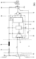
- a known circuit arrangement for headlight range control of a motor vehicle headlight shows Figure 5.
- the circuit is structured as follows.
- a setpoint generator 14 is connected in the form of a transmitter potentiometer.
- This setpoint generator 14 is located in the area of the dashboard A of the motor vehicle.
- the center tap of the setpoint generator 14 and the supply voltage terminal 1 are connected to a headlamp leveling device C mechanically coupled to the headlight 10 via suitable feed lines B.
- the supply lines B are represented in an equivalent circuit by the series connection of a resistor 16 with a downstream coil 18.
- the headlamp leveling device C has a drive motor 12 for adjusting the height and / or inclination of the headlight 10. The adjustment is indicated schematically by the arrow P.
- An actual value transmitter 28, here a so-called feedback potentiometer, is coupled to the headlight 10, between its center tap and the reference potential terminal 3 a signal V FB, which is representative of the current position of the headlight 10, can be grasped.
- the headlight range adjuster C has a control device IC with an input-side comparison stage 20 and an output-side driver stage 24, to which the drive motor 12 is connected.
- a logic unit 22 is connected between the comparison stage 20, which is regularly subject to hysteresis, and the driver stage 24. To supply voltage to the comparison stage 20, the logic unit 22 and the driver stage 24, these are connected with leads to the supply voltage V S provided via the series connection of the resistor 16 and the coil 18 and to reference potential.
- An electrolytic capacitor which will be explained in more detail, is connected between the reference potential terminal 3 and the line for the supply voltage V S.
- the comparison stage 20 is connected with its one input terminal to the center tap of the setpoint generator 14 and receives a setpoint signal V 14 from there. At the other input terminal, the comparison stage 20 receives the actual signal V FB and forms a differential voltage ⁇ V at its output, which is subject to hysteresis.
- the setpoint device on the dashboard A enables the driver of the motor vehicle to individually adjust the headlight position. Due to the necessary mechanical coupling of the motor 12 and the actual value transmitter 28 with the headlight 10, the headlight range adjuster C is accommodated directly on the headlight 10.
- the drive motor 12 is driven by the driver stage 24, which is preferably a full-bridge circuit. Depending on the position of the setpoint generator 14, the headlamp 10 is to be more or less faded in or out, that is to say its inclination angle is adjusted.
- the actual value transmitter 28 is used as an angle sensor. This delivers the actual signal V FB and is mechanical with the drive motor 12 and z. B. connected via a worm drive with the pitching mechanism of the headlight 10.
- the signal V 14 supplied from the reference value generator 14 is compared in the comparator 20 with the signal V FB. Depending on the differential voltage V, the drive motor 12 rotates and changes the signal V FB until the differential signal ⁇ V becomes zero.
- the invention has the aim of a method and a circuit arrangement for headlight range adjustment indicate the use of an electrolytic capacitor with high capacity makes it unnecessary and therefore small to be built.
- the invention essentially sees an additional device before, the result of a Actual / target comparison of the control loop for a given one Time blocked and thus hidden.
- the output signal the comparison level remains within the control device for this time without effect.
- the circuit arrangement shown in Fig. 1 corresponds to to the differences in the circuit arrangement explained below of Fig. 5.
- the crucial difference to 5 consists in the circuit arrangement 1 in that in the control device IC, which is preferably designed as an integrated circuit, a fade-out device 30 which is connected to the logic unit 22 is coupled in a manner yet to be explained.
- the blanking device 30 receives a signal from logic unit 22 START, processes this signal and directs the logic unit 22 a signal BLANK.
- the masking device 30 is via a capacitor 40 which is outside the control device IC is arranged, connected to reference potential.
- the capacitor 26 now not as an electrolytic capacitor, but as Capacitor formed with a relatively low capacitance is.
- the capacitor 26 also serves as a filter capacitor, can be reduced to some 100 nF, however. So that is the use of an inexpensive, small temperature-resistant SMD-capable (surface mounted device) and reliable ceramic Capacity possible.
- the masking device 30 ensures that the output signal the comparison stage 20 for a predetermined period of time remains ineffective and is therefore hidden.
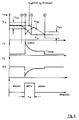
- the main voltage and current profiles are shown in FIG. 2 for a better understanding of this function. This will be discussed further below.
- the fade-out time can be individually adapted to the respective application with a ceramic capacitor of relatively low capacitance (cf. FIG. 3).
- the capacitor 26 is still required to limit the voltage change rate (dV S / dt). Too high a rate of voltage change (“slew rate”) has repercussions from the driver stage 24 on the logic unit 22 and the comparison stage 20. Such reactions occur particularly when the control device IC is monolithically integrated in a semiconductor body.
- FIG. 2 four time diagrams of voltage and current profiles are shown with respect to one another.
- the uppermost curve shows the voltage signal V 14 , which, starting from a higher value at time a, is gradually reduced to a lower value by corresponding actuation of the setpoint generator 14 (cf. FIG. 1). This lower value is reached at time c.
- V HY denotes the hysteresis voltage of comparison stage 20.
- signal V 14 reaches the lower hysteresis value of comparison stage 20.
- drive motor 12 starts.
- Motor current I M jumps to high blocking current I STALL at time b and then to drop to the nominal current I NENN with the mechanical time constant.
- V S drops abruptly at time b.
- the actual value signal V FB breaks in accordance with the dashed line in the upper signal diagram at time b and drops significantly below the desired signal V 14 .
- the drive motor 12 would be stopped in this case and controlled in reverse since V FB ⁇ (V 14 -1/2 V HY ) is.
- the masking device 30 ensures that the output signal of the comparison stage 20 is suppressed for a predetermined period of time immediately after the start of the drive motor 12, ie at time b.
- the predetermined period of time is selected such that V FB > V 14 is in any case after the period of time has elapsed.
- the fade-out time t A is chosen to be so long that its end is somewhat after the time c.
- the signal V FB jumps suddenly below V 14 at the time b and then gradually rises again. After the blanking time t A , the signal V FB drops until the time d at which the drive motor 12 is switched off.
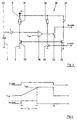
- FIG. 3 shows an exemplary embodiment of the masking device 30 from FIG. 1.
- the circuit has the capacitor 40 already explained, which can have, for example, a capacitance value of 47 nF and is connected with one connection to the reference potential terminal 3 and with its other connection to a terminal of the control device.
- This terminal is designated by the reference symbol K and, within the masking device 30, is connected to the non-inverting input of a comparator 38.
- the inverting input of the comparator 38 is in contact with a reference voltage V REF .
- the terminal K is also connected via a current source 31 to the supply voltage terminal 5 for the supply voltage V S.
- Terminal K is additionally connected to reference potential terminal 3 via the load path of a bipolar transistor 32.
- the output terminal of the comparator 38 is connected to the control terminal of a second transistor 34.
- the load path of this second transistor 34 lies between the reference potential terminal 3 and a terminal at which the BLANK signal can be tapped.
- This terminal is connected to the supply voltage terminal 5 via a resistor 37.
- this terminal is connected to the reference potential terminal 3 via the load path of a third transistor 35.
- the control connection of this third transistor 35 is connected to the control connection of the first transistor 32 and is connected to the reference potential terminal 3 via the load path of a fourth transistor 33.
- the connection point of the two control connections of the transistors 32, 35 is also connected to the supply voltage terminal 5 via a resistor 36.
- the control connection of the fourth transistor is connected to a terminal for the START signal.
- the resistors 36, 37 mentioned can also be replaced by current sources.
- this masking device 30 becomes clear in connection with the signal profiles of FIG. 4. If the difference V 14 - V FB (cf. FIG. 1) is greater than the switching hysteresis of the comparison stage 20, the signal START is generated, which clamps the bases of the transistors 32 and 35 via the transistor 33. As a result, the charging process of the capacitor 40 is started, as a result of which the voltage V 40 dropping across it increases. With the start of the START signal, the BLANK signal also begins at time t 0 . If the voltage V 40 reaches the reference voltage V ref , the signal BLANK is set to a low "low" level again by the transistor 34. The time period t 1 -t 0 is the blanking time t A.
- the logic unit 22 of the control device IC ensures that the output signal of the comparison stage 20 is masked out. If the signal V 14 becomes equal to the signal V FB , which is the case at time t 2 , the signal START is reset and the capacitor 40 is discharged via the transistor 32.
Landscapes
- Engineering & Computer Science (AREA)
- Mechanical Engineering (AREA)
- Lighting Device Outwards From Vehicle And Optical Signal (AREA)
Abstract
Description
Die Erfindung betrifft ein Verfahren zur Leuchtweitenregulierung
eines Scheinwerfers gemäß dem Oberbegriff des Anspruchs
1 sowie eine Schaltungsanordnung gemäß dem Oberbegriff des
Anspruchs 7.The invention relates to a method for headlight range control
a headlamp according to the preamble of the
Bei den heute hergestellten Kraftfahrzeugen ist regelmäßig die Leuchtweitenregulierung der Scheinwerfer vorgesehen. Eine Leuchtweitenregulierung ist deshalb notwendig, damit die Scheinwerfer je nach Beladungszustand des Kfz so eingestellt sind, daß ein Gegenverkehr nicht geblendet wird. In Kraftfahrzeugen sind hierfür entweder stufenlose Leuchtweitensteller oder schaltbare Leuchtweitensteller üblich.In today's motor vehicles is regular the headlight range adjustment is provided. A Headlight range control is therefore necessary so that the Headlights adjusted depending on the load of the vehicle are that oncoming traffic is not dazzled. In motor vehicles are either continuous headlamp levelers or switchable headlamp leveling is common.
Eine bekannte Schaltungsanordnung für eine Leuchtweitenregulierung eines Kfz-Scheinwerfers zeigt Figur 5. Die Schaltung ist folgendermaßen aufgebaut.A known circuit arrangement for headlight range control of a motor vehicle headlight shows Figure 5. The circuit is structured as follows.
Zwischen eine Versorgungsspannungsklemme 1, an der die Betriebsspannung
VB und damit also die Batteriespannung eines
Kfz anliegt, und eine Bezugspotentialklemme 3 ist ein Sollwertgeber
14 in Form eines Geber-Potentiometers geschaltet.
Dieser Sollwertgeber 14 befindet sich im Bereich des Armaturenbretts
A des Kfzs. Über geeignete Zuleitungen B ist der
Mittenabgriff des Sollwertgebers 14 und die Versorgungsspannungsklemme
1 mit einem an den Scheinwerfer 10 mechanisch
gekoppelten Leuchtweitensteller C verbunden. Die Zuleitungen
B sind der Einfachheit halber durch die Serienschaltung eines
Widerstandes 16 mit nachgeschalteter Spule 18 ersatzschaltbildlich
dargestellt. Der Leuchtweitensteller C weist
einen Antriebsmotor 12 zum Höhen- und/oder Neigungsverstellen
des Scheinwerfers 10 auf. Die Verstellung ist durch den Pfeil
P schematisch angedeutet. Mit dem Scheinwerfer 10 ist ein
Istwertgeber 28, hier ein sogenanntes Feedback-Potentiometer,
gekoppelt, zwischen dessen Mittenabgriff und Bezugspotentialklemme
3 ein für die augenblickliche Stellung des Scheinwerfers
10 repräsentatives Signal VFB greifbar ist. Der
Leuchtweitensteller C verfügt über eine Steuereinrichtung IC
mit einer eingangsseitigen Vergleichsstufe 20 und einer ausgangsseitigen
Treiberstufe 24, an die der Antriebsmotor 12
geschaltet ist. Zwischen der Vergleichsstufe 20, die regelmäßig
hysteresebehaftet ist, und der Treiberstufe 24 ist eine
Logikeinheit 22 geschaltet. Zur Spannungsversorgung der Vergleichsstufe
20, der Logikeinheit 22 und der Treiberstufe 24
sind diese mit Zuleitungen an die über die Serienschaltung
des Widerstandes 16 und der Spule 18 bereitgestellte Speisespannung
VS und an Bezugspotential angeschlossen. Zwischen
der Bezugspotentialklemme 3 und der Leitung für die Speisespannung
VS ist ein Elektrolytkondensator, der noch näher erläutert
wird, angeschlossen. Die Vergleichsstufe 20 ist mit
ihrer einen Eingangsklemme an den Mittenabgriff des Sollwertgebers
14 angeschlossen und erhält von dort ein Sollsignal
V14. An der andere Eingangsklemme erhält die Vergleichsstufe
20 das Istsignal VFB und bildet an ihrem Ausgang hysteresebehaftet
eine Differenzspannung ΔV.Between a
Die Funktionsweise ist folgendermaßen. The way it works is as follows.
Der Sollwertgeber am Armaturenbrett A ermöglicht dem Fahrer
des Kfz die individuelle Justage der Scheinwerferstellung.
Aufgrund der notwendigen mechanischen Kopplung des Motors 12
und des Istwertgebers 28 mit dem Scheinwerfer 10 ist der
Leuchtweitensteller C direkt am Scheinwerfer 10 untergebracht.
Der Antriebsmotor 12 wird von der Treiberstufe 24,
die vorzugsweise eine Vollbrückenschaltung ist, angetrieben.
Je nach Stellung des Sollwertgebers 14 soll der Scheinwerfer
10 mehr oder weniger auf- oder abgeblendet, also dessen Neigungswinkel
verstellt werden. Dazu wird der Istwertgeber 28
als Winkelaufnehmer benutzt. Dieser liefert das Istsignal VFB
und ist mechanisch mit dem Antriebsmotor 12 und z. B. über
einen Schneckenantrieb mit der Nickmechanik des Scheinwerfers
10 verbunden. Das vom Sollwertgeber 14 gelieferte Signal V14
wird in der Vergleichsstufe 20 mit dem Signal VFB verglichen.
Je nach Differenzspannung V dreht der Antriebsmotor 12 so
lange und verändert das Signal VFB bis das Differenzsignal
ΔV zu null wird.The setpoint device on the dashboard A enables the driver of the motor vehicle to individually adjust the headlight position. Due to the necessary mechanical coupling of the
Da das gesamte System eine gewisse Massenträgheit aufweist,
wird der Abgleich zwischen Sollwertgeber 14 und Istwertgeber
28 durch ein "Ausrollen" und damit einer Weiterbelegung des
Antriebsmotors 12 verfälscht. Dies kann zu unerwünschten
Kippschwingungen des gesamten Systems führen. Ferner führt
die Anordnung bei kleinsten Störspannungen unerwünschte
Stellbewegungen aus.Since the entire system has a certain inertia,
becomes the comparison between
Weil der Sollwertgeber 14 und der Istwertgeber 28 an zwei
verhältnismäßig weit voneinander entfernten Orten installiert
ist, ist des Weiteren die Einstreuung von Störungen über die
Zuleitungen B hochwahrscheinlich. Da die Betriebsspannung VB
direkt an dem Sollwertgeber 14 angelegt ist und die übrige
Schaltung über die Zuleitungsimpedanz versorgt wird, bricht
bei jedem Start des Antriebsmotors 12 die Speisespannung VS
ein. Es entsteht eine unerwünschte Eingangsspannungsdifferenz
an der Vergleichsstufe 20, was gezwungenermaßen zu Kippschwingungen
am Scheinwerfer 10 aufgrund des unerwünschten
Hin- und Herantriebes des Motors 12 bewirkt. Eine solche
Kippschwingung hat darüber hinaus eine deutlich erhöhte Leistungsaufnahme
zur Folge und kann evtl. sogar zu einer Überhitzung
der Treiberstufe 24 führen.Furthermore, since the
Dieses Problem wurde im Wesentlichen dadurch gelöst, daß die
Vergleichsstufe 20 mit einer Hysterese versehen ist. Zusätzlich
muß jedoch die Speisespannung VS mit einem relativ großen
Elektrolytkondensator (vgl. in Fig. 5, Bezugszeichen 26)
gegen Masse gesiebt werden. Dieser Elektrolytkondensator 26
ist teuer und zeichnet sich nur durch einen eingeschränkten
Temperaturbereich aus. Darüber hinaus ist ein solcher Elektrolytkondensator
mit einer entsprechend großen Kapazität
nicht als SMD-Bauelement verfügbar und läuft daher einer zunehmenden
Miniaturisierung der Schaltung zuwider. Schließlich
können solche Elektrolytkondensatoren bei hartem Einsatz, wie
er im Kfz regelmäßig gegeben ist, auch austrocknen, so daß
deren Zuverlässigkeit unsicher ist. Für eine akzeptable
Leuchtweitenregulierung ist es dennoch erforderlich, einen
solchen Elektrolytkondensator mit hoher Kapazität und damit
großem Siebfaktor zu verwenden, um Kippschwingungen des
Scheinwerfers 10 sicher zu unterdrücken. This problem was essentially solved by providing the
Die Erfindung hat das Ziel, ein Verfahren und eine Schaltungsanordnung zur Leuchtweitenregulierung eines Scheinwerfers anzugeben, das die Verwendung eines Elektrolytkondensators mit hoher Kapazität entbehrlich macht und daher klein bauend zu realisieren ist.The invention has the aim of a method and a circuit arrangement for headlight range adjustment indicate the use of an electrolytic capacitor with high capacity makes it unnecessary and therefore small to be built.
Diese Aufgabe wird für das Verfahren durch die Merkmale des
Anspruchs 1 und für die Schaltungsanordnung durch die Merkmale
des Anspruchs 7 gelöst.This task is carried out for the process by the characteristics of
Weiterbildungen der Erfindung sind Gegenstand der Unteransprüche.Developments of the invention are the subject of the dependent claims.
Die Erfindung sieht im Wesentlichen eine Zusatzeinrichtung vor, die bei jedem Start des Antriebsmotors das Ergebnis eines Ist-/Soll-Vergleiches des Regelkreises für eine vorgegebene Zeit blockiert und damit ausblendet. Das Ausgangssignal der Vergleichsstufe innerhalb der Steuereinrichtung bleibt für diese Zeit ohne Wirkung.The invention essentially sees an additional device before, the result of a Actual / target comparison of the control loop for a given one Time blocked and thus hidden. The output signal the comparison level remains within the control device for this time without effect.
Das Verfahren und die Schaltungsanordnung werden nachfolgend im Zusammenhang mit einem Ausführungsbeispiel anhand der Zeichnung näher erläutert. Es zeigen:
- Fig. 1
- das Blockschaltbild eines Ausführungsbeispieles einer Schaltungsanordnung zur Leuchtweitenregulierung eines Scheinwerfers gemäß vorliegender Erfindung,
- Fig. 2
- die wesentlichen Spannungs- und Stromverläufe in der Schaltungsanordnung von Fig. 1,
- Fig. 3
- ein Ausführungsbeispiel für eine in der Steuereinrichtung von Fig. 1 eingesetzte Ausblendeinrichtung,
- Fig. 4
- Signalverläufe zu der Schaltungsanordnung von Fig. 3, und
- Fig. 5
- die bereits erläuterte Schaltungsanordnung zur Leuchtweitenregulierung eines Scheinwerfers nach dem Stand der Technik.
- Fig. 1
- 2 shows the block diagram of an exemplary embodiment of a circuit arrangement for regulating the headlight range of a headlight according to the present invention,
- Fig. 2
- the essential voltage and current profiles in the circuit arrangement of Fig. 1,
- Fig. 3
- 1 shows an exemplary embodiment of a masking device used in the control device of FIG. 1,
- Fig. 4
- Waveforms to the circuit arrangement of Fig. 3, and
- Fig. 5
- the already explained circuit arrangement for headlight range control of a headlight according to the prior art.
In den nachfolgenden Figuren bezeichnen, sofern nicht anders angegeben, gleiche Bezugszeichen gleiche Teile mit gleicher Bedeutung. Die bereits im Zusammenhang mit der Erläuterung von Fig. 5 benutzten Bezugszeichen gelten für gleiche Teile mit gleicher Bedeutung weiter.Designate in the following figures, unless otherwise indicated, same reference numerals, same parts with the same Meaning. The already in connection with the explanation 5 used for the same parts continue with the same meaning.
Die in Fig. 1 dargestellte Schaltungsanordnung entspricht bis
auf die nachfolgend erläuterten Unterschiede der Schaltungsanordnung
von Fig. 5. Der entscheidende Unterschied zur
Schaltungsanordnung von Fig. 5 besteht in der Schaltungsanordnung
von Fig. 1 darin, daß in der Steuereinrichtung IC,
die vorzugsweise als integrierter Schaltkreis ausgeführt ist,
eine Ausblendeinrichtung 30 sitzt, welche mit der Logikeinheit
22 in noch zu erläuternder Weise gekoppelt ist. Die Ausblendeinrichtung
30 empfängt von der Logikeinheit 22 ein Signal
START, verarbeitet dieses Signal und leitet der Logikeinheit
22 ein Signal BLANK zu. Die Ausblendeinrichtung 30
ist über einen Kondensator 40, der außerhalb der Steuereinrichtung
IC angeordnet ist, an Bezugspotential geschaltet. The circuit arrangement shown in Fig. 1 corresponds to
to the differences in the circuit arrangement explained below
of Fig. 5. The crucial difference to
5 consists in the
Ein weiterer wesentlicher Unterschied ist, daß der Kondensator
26 jetzt nicht als Elektrolytkondensator, sondern als
Kondensator mit verhältnismäßig geringer Kapazität ausgebildet
ist. Der Kondensator 26 dient ebenfalls als Siebkondensator,
kann jedoch auf einige 100 nF verringert sein. Damit ist
der Einsatz einer preiswerten, kleinen temperaturfesten SMD-fähigen
(surface mounted device) und zuverlässigen keramischen
Kapazität möglich.Another major difference is that the
Die Ausblendeinrichtung 30 sorgt dafür, daß das Ausgangssignal
der Vergleichsstufe 20 für eine vorgegebene Zeitspanne
ohne Wirkung bleibt und damit ausgeblendet ist.The masking
Zum besseren Verständnis dieser Funktion sind die wichtigsten
Spannungs- und Stromverläufe in Fig. 2 dargestellt. Hierauf
wird noch weiter unten eingegangen. Nach der vorgegebenen
Zeitspanne der Ausblendung arbeitet die Schaltungsanordnung
wieder, ohne daß die Ausblendeinrichtung 30 weiter Einfluß
nimmt. Die Ausblendzeit kann mit einem keramischen Kondensator
verhältnismäßig geringer Kapazität individuell an die jeweilige
Applikation angepaßt werden (vgl. hierzu Fig. 3). Der
Kondensator 26 ist noch erforderlich, um die Spannungsänderungsgeschwindigkeit
(dVS/dt) zu limitieren. Eine zu hohe
Spannungsänderungsgeschwindigkeit ("Slew-rate") hat Rückwirkungen
von der Treiberstufe 24 auf die Logikeinheit 22 und
der Vergleichsstufe 20 zur Folge. Solche Rückwirkungen treten
insbesondere dann auf, wenn die Steuereinrichtung IC monolithisch
in einen Halbleiterkörper integriert ist.The main voltage and current profiles are shown in FIG. 2 for a better understanding of this function. This will be discussed further below. After the predetermined period of the blanking, the circuit arrangement operates again without the blanking
In Fig. 2 sind untereinander vier Zeitdiagramme von Spannungs- und Stromverläufen in zeitlicher Beziehung zueinander
untereinander dargestellt. In der obersten Kurve ist das
Spannungssignal V14 dargestellt, das ausgehend von einem höheren
Wert zum Zeitpunkt a allmählich auf einen niedrigeren
Wert durch entsprechende Betätigung des Sollwertgebers 14
(vgl. hierzu Fig. 1) reduziert wird. Zum Zeitpunkt c ist dieser
niedrigere Wert erreicht. Mit VHY ist die Hysteresespannung
der Vergleichsstufe 20 bezeichnet. Zum Zeitpunkt b, der
zwischen den Zeitpunkten a und c liegt, erreicht das Signal
V14 den unteren Hysteresewert der Vergleichsstufe 20. Zum
Zeitpunkt b startet der Antriebsmotor 12. Der Motorstrom IM
springt zum Zeitpunkt b auf den hohen Blockierstrom ISTALL,
um anschließend mit der mechanischen Zeitkonstanten auf den
Nennstrom INENN abzusinken.In FIG. 2, four time diagrams of voltage and current profiles are shown with respect to one another. The uppermost curve shows the voltage signal V 14 , which, starting from a higher value at time a, is gradually reduced to a lower value by corresponding actuation of the setpoint generator 14 (cf. FIG. 1). This lower value is reached at time c. V HY denotes the hysteresis voltage of
Die Speisespannung VS sinkt zum Zeitpunkt b abrupt ab. Das
Istwertsignal VFB bricht entsprechend der strichlierten Linie
im oberen Signaldiagramm zum Zeitpunkt b ein und sinkt deutlich
unter das Sollsignal V14. Ohne die erfindungsgemäße Ausblendeinrichtung
30 und damit bei einer Schaltungsanordnung
nach dem Stand der Technik würde der Antriebsmotor 12 in diesem
Fall gestoppt und rückwärts gesteuert, da
Erfindungsgemäß sorgt jedoch die Ausblendeinrichtung 30 dafür,
daß unmittelbar nach dem Start des Antriebsmotors 12,
also zum Zeitpunkt b, das Ausgangssignal der Vergleichsstufe
20 für eine vorgegebene Zeitspanne unterdrückt wird. Die vorgegebene
Zeitspanne ist so gewählt, daß auf jeden Fall nach
Ablauf der Zeitspanne VFB > V14 ist. Im dargestellten Ausführungsbeispiel
von Fig. 2 ist die Ausblendzeit tA so groß gewählt,
daß deren Ende etwas nach dem Zeitpunkt c liegt. Wie
im obersten Zeitdiagramm von Fig. 2 dargestellt, springt also
das Signal VFB zum Zeitpunkt b sprungartig unter V14, um dann
allmählich wieder anzusteigen. Nach der Ausblendzeit tA sinkt
das Signal VFB bis zum Zeitpunkt d, zu dem der Antriebsmotor
12 abgeschaltet wird.According to the invention, however, the masking
In Fig. 3 ist ein Ausführungsbeispiel der Ausblendeinrichtung
30 von Fig. 1 dargestellt. Die Schaltung weist den bereits
erläuterten Kondensator 40 auf, der beispielsweise einen Kapazitätswert
von 47 nF haben kann und mit einem Anschluß mit
der Bezugspotentialklemme 3 und mit seinem anderen Anschluß
an eine Klemme der Steuereinrichtung angeschlossen ist. Diese
Klemme ist mit dem Bezugszeichen K bezeichnet und innerhalb
der Ausblendeinrichtung 30 mit dem nicht invertierenden Eingang
eines Vergleichers 38 in Verbindung. Der invertierende
Eingang des Vergleichers 38 ist mit einer Referenzspannung
VREF in Kontakt. Die Klemme K ist darüber hinaus über eine
Stromquelle 31 an die Speisespannungsklemme 5 für die Speisespannung
VS geschaltet. Die Klemme K ist zusätzlich über die
Laststrecke eines Bipolartransistors 32 an die Bezugspotentialklemme
3 geschaltet. Die Ausgangsklemme des Vergleichers 38
ist mit dem Steueranschluß eines zweiten Transistors 34 in
Verbindung. Die Laststrecke dieses zweiten Transistors 34
liegt zwischen der Bezugspotentialklemme 3 und einer Klemme,
an der das Signal BLANK abgreifbar ist. Diese Klemme ist über
einen Widerstand 37 mit der Speisespannungsklemme 5 in Verbindung.
Zusätzlich ist diese Klemme über die Laststrecke eines
dritten Transistors 35 an die Bezugspotentialklemme 3 geschaltet.
Der Steueranschluß dieses dritten Transistors 35
ist mit dem Steueranschluß des ersten Transistors 32 in Verbindung
und über die Laststrecke eines vierten Transistors 33
an Bezugspotentialklemme 3 geschaltet. Der Verbindungspunkt
der beiden Steueranschlüsse der Transistoren 32, 35 ist des
Weiteren über einen Widerstand 36 an die Speisespannungsklemme
5 gelegt. Der Steueranschluß des vierten Transistors ist
mit einer Klemme für das Signal START in Verbindung. Die erwähnten
Widerstände 36, 37 können auch durch Stromquellen ersetzt
sein.FIG. 3 shows an exemplary embodiment of the
Die Funktionsweise dieser Ausblendeinrichtung 30 wird im Zusammenhang
mit den Signalverläufen von Fig. 4 deutlich. Wird
die Differenz V14 - VFB (vgl. hierzu Fig. 1) größer als die
Schalthysterese der Vergleichsstufe 20, so wird das Signal
START erzeugt, was über den Transistor 33 die Basen der Transistoren
32 und 35 klemmt. Hierdurch wird der Ladevorgang des
Kondensators 40 gestartet, wodurch die an ihm abfallende
Spannung V40 ansteigt. Mit dem Beginn des Signales START beginnt
auch das Signal BLANK zum Zeitpunkt t0. Erreicht die
Spannung V40 die Referenzspannung Vref, wird das Signal BLANK
durch den Transistor 34 wieder auf niedrigen Pegel "Low" gesetzt.
Die Zeitspanne t1-t0 ist die Ausblendzeit tA. Während
das Signal BLANK einen hohen Pegel "high" einnimmt, sorgt die
Logikeinheit 22 der Steuereinrichtung IC dafür, daß das Ausgangssignal
der Vergleichsstufe 20 ausgeblendet wird. Wird
das Signal V14 gleich dem Signal VFB, was zum Zeitpunkt t2
der Fall ist, wird das Signal START rückgesetzt und der Kondensator
40 über den Transistor 32 entladen. The mode of operation of this
Es ist hier noch abschließend anzumerken, daß die Schaltung nicht notwendigerweise nur zur Leuchtweitenregulierung von Scheinwerfern eingesetzt werden kann. Vielmehr findet das erfindungsgemäße Verfahren und die vorgestellte Schaltungsanordnung auch überall dort sinnvoll Anwendung, wo es darauf ankommt, daß ein Motor ohne unerwünschte Hin- und Herbewegung anlaufen muß. Solche Motoren werden allgemein als Servomotoren bezeichnet.Finally, it should be noted that the circuit not only for headlight range adjustment from Headlights can be used. Rather, the invention Method and the circuit arrangement presented Also useful wherever there is application arrives that an engine with no undesirable reciprocation must start. Such motors are commonly called servomotors designated.
Claims (15)
dadurch gekennzeichnet, daß nach jedem Start des Antriebsmotors (12) das Ergebnis des Ist-/Soll-Vergleiches für eine vorgegebene Zeitspanne (tA) ignoriert und damit ausgeblendet wird.Method for regulating the headlight range of a headlight (10), in which a drive motor (12) mechanically coupled to the headlight (10) for adjusting the headlight (10) is driven as a function of a control signal obtained from an actual / target comparison,
characterized in that after each start of the drive motor (12) the result of the actual / target comparison is ignored for a predetermined period of time (t A ) and is therefore hidden.
dadurch gekennzeichnet, daß das Stellsignal als Differenzsignal eines von einer manuell zu betätigenden Verstelleinrichtung (14) kommenden Soll-Signales (V14) und einem die augenblickliche Stellung des Scheinwerfers (10) entsprechenden Ist-Signales (VFB) abgeleitet wird.Method according to claim 1,
characterized in that one of the setting signal from a manually coming operable adjusting device (14) desired signal (V 14) and a the instantaneous position of the headlight (10) corresponding actual signal (V FB) is derived as a differential signal.
dadurch gekennzeichnet, daß das Stellsignal hysteresebehaftet ist.The method of claim 1 or 2,
characterized in that the control signal is subject to hysteresis.
dadurch gekennzeichnet, daß die vorgegebene Zeitspanne (tA) einstellbar ist.Method according to one of claims 1 to 3,
characterized in that the predetermined time period (t A ) is adjustable.
dadurch gekennzeichnet, daß der Beginn (t0) der Zeitspanne (tA) durch eine vorgegebene Größe des Differenzsignales bestimmt ist und das Ende (t1) der Zeitspanne (tA) dann erreicht ist, wenn ein Kondensator (40) auf eine vorgegebene Referenzspannung (Vref) aufgeladen worden ist.Method according to one of claims 1 to 4,
characterized in that the start (t 0 ) of the time period (t A ) is determined by a predetermined size of the difference signal and the end (t 1 ) of the time period (t A ) is reached when a capacitor (40) to a predetermined one Reference voltage (V ref ) has been charged.
dadurch gekennzeichnet, daß ein Rücksetzsignal für einen neuen Beginn (t0) der Zeitspanne (tA) erzeugt wird, wenn das Differenzsignal mindestens annähernd gleich oder gleich 0 ist.Method according to claim 5,
characterized in that a reset signal for a new beginning (t 0 ) of the time period (t A ) is generated when the difference signal is at least approximately equal to or equal to 0.
gekennzeichnet durch das weitere Merkmal:
characterized by the further characteristic:
dadurch gekennzeichnet, daß die Steuereinrichtung (IC) eingangsseitig eine Vergleichsstufe (20) und ausgangsseitig eine Treiberstufe (24) sowie eine zwischen die Vergleichsstufe (20) und die Treiberstufe (24) geschaltete Logikeinheit (22) aufweist.Circuit arrangement according to claim 7,
characterized in that the control device (IC) has a comparison stage (20) on the input side and a driver stage (24) on the output side and a logic unit (22) connected between the comparison stage (20) and the driver stage (24).
dadurch gekennzeichnet, daß der Istwertgeber (14) und/oder der Sollwertgeber (28) durch Potentiometer gebildet ist, wobei der Mittelabgriff oder die Mittelabgriffe des oder der Potentiometer mit der Vergleichsstufe (20) der Steuereinrichtung (IC) gekoppelt ist.Circuit arrangement according to claim 7 or 8,
characterized in that the actual value transmitter (14) and / or the setpoint transmitter (28) is formed by a potentiometer, the center tap or the center taps of the potentiometer (s) being coupled to the comparison stage (20) of the control device (IC).
dadurch gekennzeichnet, daß die Ausblendeinrichtung (30) einen für die Zeitspanne (tA) maßgebenden Kondensator (40) und einen Vergleicher (38) aufweist, und daß der Vergleicher (38) eingangsseitig einerseits mit einer Referenzspannung (Vref) beaufschlagbar und andererseits an den Kondensator (40) angeschlossen ist.Circuit arrangement according to one of claims 7 to 9,
characterized in that the blanking device (30) has a capacitor (40) and a comparator (38) which is decisive for the time span (t A ), and in that the comparator (38) can be supplied with a reference voltage (V ref ) on the input side and on the other side the capacitor (40) is connected.
dadurch gekennzeichnet, daß die Ausblendeinrichtung (30) die Serienschaltung einer zwischen eine Versorgungsspannungsklemme (1) und Bezugspotentialklemme (3) geschalteten Reihenschaltung einer Stromquelle (31) und der Laststrecke eines Transistors (32) aufweist, daß der Kondensator (40) zwischen die Bezugspotentialklemme (3) und den Mittenabgriff der Reihenschaltung der Stromquelle (31) und des Transistors (32) geschaltet, daß der Mittenabgriff mit einer ersten Eingangsquelle des Vergleichers (38) verbunden ist, daß eine andere Eingangsklemme des Vergleichers (38) an die Referenzspannung (Vref) ankoppelbar ist, daß der Ausgang des Vergleichers (38) mit dem Steueranschluß eines zweiten Transistors (34) verbunden ist, daß die Laststrecke dieses zweiten Transistors (34) zwischen der Bezugspotentialklemme (3) und einer Ausgangsklemme für ein Ausgangssignal (BLANK) der Ausblendeinrichtung (30) verbunden ist, daß diese Ausgangsklemme über einen Widerstand (37) mit der Versorgungsspannungsklemme (1) und über die Laststrecke eines dritten Transistors (35) mit der Bezugspotentialklemme (3) in Verbindung steht, daß der Steueranschluß dieses dritten Transistors (35) mit dem Steueranschluß des ersten Transistors (32) verbunden ist und über die Laststrecke eines vierten Transistors (33) an die Bezugspotentialklemme (3) und über einen weiteren Widerstand (36) an die Versorgungsspannungsklemme (1) geschaltet ist, und daß der Steueranschluß des vierten Transistors (33) mit einer Eingangsklemme für ein Eingangssignal (START) der Ausblendeinrichtung (30) in Verbindung steht.Circuit arrangement according to one of claims 7 to 10,
characterized in that the blanking device (30) has the series connection of a series connection of a current source (31) connected between a supply voltage terminal (1) and reference potential terminal (3) and the load path of a transistor (32), that the capacitor (40) between the reference potential terminal ( 3) and the center tap of the series connection of the current source (31) and the transistor (32) that the center tap is connected to a first input source of the comparator (38), that another input terminal of the comparator (38) to the reference voltage (V ref ) can be coupled, that the output of the comparator (38) is connected to the control connection of a second transistor (34), that the load path of this second transistor (34) between the reference potential terminal (3) and an output terminal for an output signal (BLANK) of the masking device (30) is connected that this output terminal via a resistor (37) to the supply voltage terminal (1) and via the load path of a third transistor (35) with the reference potential terminal (3) in connection that the control terminal of this third transistor (35) is connected to the control terminal of the first transistor (32) and over the load path of a fourth Transistor (33) is connected to the reference potential terminal (3) and via a further resistor (36) to the supply voltage terminal (1), and that the control connection of the fourth transistor (33) with an input terminal for an input signal (START) of the masking device (30 ) is connected.
dadurch gekennzeichnet, daß mindestens einer der Widerstände (36, 37) durch Stromquellen realisiert ist.Circuit arrangement according to claim 11,
characterized in that at least one of the resistors (36, 37) is realized by current sources.
dadurch gekennzeichnet, daß die Steuereinrichtung (IC) als integrierter Schaltkreis ausgebildet ist.Circuit arrangement according to one of claims 7 to 12,
characterized in that the control device (IC) is designed as an integrated circuit.
dadurch gekennzeichnet, daß die Vergleichsstufe (20) eine Schalthysterese aufweist.Circuit arrangement according to one of claims 7 to 13,
characterized in that the comparison stage (20) has a switching hysteresis.
dadurch gekennzeichnet, daß der Scheinwerfer (10) ein Kfz-Scheinwerfer ist.Circuit arrangement according to one of claims 7 to 14,
characterized in that the headlight (10) is a motor vehicle headlight.
Applications Claiming Priority (2)
| Application Number | Priority Date | Filing Date | Title |
|---|---|---|---|
| DE1997143260 DE19743260C2 (en) | 1997-09-30 | 1997-09-30 | Method and circuit arrangement for headlight range control |
| DE19743260 | 1997-09-30 |
Publications (3)
| Publication Number | Publication Date |
|---|---|
| EP0904981A2 true EP0904981A2 (en) | 1999-03-31 |
| EP0904981A3 EP0904981A3 (en) | 2003-04-16 |
| EP0904981B1 EP0904981B1 (en) | 2007-12-12 |
Family
ID=7844190
Family Applications (1)
| Application Number | Title | Priority Date | Filing Date |
|---|---|---|---|
| EP19980114238 Expired - Lifetime EP0904981B1 (en) | 1997-09-30 | 1998-07-28 | Method and device for controlling the lighting distance of a headlamp |
Country Status (2)
| Country | Link |
|---|---|
| EP (1) | EP0904981B1 (en) |
| DE (2) | DE19743260C2 (en) |
Families Citing this family (1)
| Publication number | Priority date | Publication date | Assignee | Title |
|---|---|---|---|---|
| JP2001322484A (en) * | 2000-05-12 | 2001-11-20 | Koito Mfg Co Ltd | Motor control circuit of device for adjusting optical axis of vehicle light |
Family Cites Families (4)
| Publication number | Priority date | Publication date | Assignee | Title |
|---|---|---|---|---|
| FR2190265A5 (en) * | 1972-06-23 | 1974-01-25 | Jaeger | |
| DE2846602A1 (en) * | 1978-10-26 | 1980-05-08 | Bosch Gmbh Robert | Automatic correction system for vehicle headlight inclination - has pressure switch to release warning when system fails and includes potentiometer with indicator |
| DE3827983C1 (en) * | 1988-08-18 | 1990-02-01 | Hella Kg Hueck & Co, 4780 Lippstadt, De | |
| DE4024915A1 (en) * | 1990-08-06 | 1992-02-13 | Hella Kg Hueck & Co | METHOD AND DEVICE FOR REGULATING THE HEADLIGHT OF A MOTOR VEHICLE |
-
1997
- 1997-09-30 DE DE1997143260 patent/DE19743260C2/en not_active Expired - Fee Related
-
1998
- 1998-07-28 EP EP19980114238 patent/EP0904981B1/en not_active Expired - Lifetime
- 1998-07-28 DE DE59814136T patent/DE59814136D1/en not_active Expired - Lifetime
Non-Patent Citations (1)
| Title |
|---|
| None |
Also Published As
| Publication number | Publication date |
|---|---|
| EP0904981B1 (en) | 2007-12-12 |
| EP0904981A3 (en) | 2003-04-16 |
| DE59814136D1 (en) | 2008-01-24 |
| DE19743260C2 (en) | 1999-10-21 |
| DE19743260A1 (en) | 1999-04-08 |
Similar Documents
| Publication | Publication Date | Title |
|---|---|---|
| EP0543826B1 (en) | Process and device for driving an electromagnetic consumer | |
| DE3507130A1 (en) | DRIVER CIRCUIT FOR A MAGNETIC COIL | |
| EP0671812B1 (en) | Circuit arrangement for controlling the speed of electric motors | |
| DE3233536A1 (en) | DEVICE FOR THE CLOCKED REGULATION OF A COIL FLOWING THROUGH | |
| DE102004026250B4 (en) | Control circuit for piezo actuators | |
| DE10057439A1 (en) | Voltage regulator has control element, comparator element and demand value circuit that derives demand signal from input voltage so it is essentially constant during load pulse | |
| EP0904981B1 (en) | Method and device for controlling the lighting distance of a headlamp | |
| DE69108187T2 (en) | Control device for the battery voltage delivered by an alternator. | |
| EP0545111A2 (en) | Device for adjusting the inclination of vehicle headlamps | |
| EP0698794A1 (en) | Under voltage detection circuit | |
| EP1718855A1 (en) | Method and device for control of a capacitive actuator | |
| EP0098460B1 (en) | Control device for an electrical actuator | |
| EP1504317B1 (en) | Power supply circuit | |
| WO2006119751A2 (en) | Method and device for electrically actuating a valve with a mechanical closing element | |
| DE2826365A1 (en) | CONTROL DEVICE FOR A SOLENOID VALVE | |
| EP1326338B1 (en) | Device for controlling an electric power component | |
| DE10202279A1 (en) | Control circuit for an actuator | |
| DE19653666A1 (en) | Process for rapid triggering of capacitive loads, including piezoelectric actuators | |
| DE3335200A1 (en) | Voltage supply device for motor vehicles | |
| EP1625663A2 (en) | Integrated circuit arrangement, and method for programming an integrated circuit arrangement | |
| DE68914218T2 (en) | Voltage commutation regulator with stabilized gain. | |
| EP0073952A2 (en) | Electronically controlled ignition system | |
| DE102004054109A1 (en) | Drive device for fuel injection apparatus used in vehicle diesel engine carries out variable setting of the interruption threshold value according to detected voltage of the piezo stack | |
| DE4215034C2 (en) | Ignition device for an internal combustion engine | |
| DE4223660C2 (en) | Device for adjusting the light beam angle of a vehicle headlight |
Legal Events
| Date | Code | Title | Description |
|---|---|---|---|
| PUAI | Public reference made under article 153(3) epc to a published international application that has entered the european phase |
Free format text: ORIGINAL CODE: 0009012 |
|
| AK | Designated contracting states |
Kind code of ref document: A2 Designated state(s): AT BE CH CY DE DK ES FI FR GB GR IE IT LI LU MC NL PT SE |
|
| AX | Request for extension of the european patent |
Free format text: AL;LT;LV;MK;RO;SI |
|
| RAP1 | Party data changed (applicant data changed or rights of an application transferred) |
Owner name: INFINEON TECHNOLOGIES AG |
|
| PUAL | Search report despatched |
Free format text: ORIGINAL CODE: 0009013 |
|
| AK | Designated contracting states |
Designated state(s): AT BE CH CY DE DK ES FI FR GB GR IE IT LI LU MC NL PT SE |
|
| AX | Request for extension of the european patent |
Extension state: AL LT LV MK RO SI |
|
| RIC1 | Information provided on ipc code assigned before grant |
Ipc: 7B 60Q 1/076 A |
|
| 17P | Request for examination filed |
Effective date: 20030625 |
|
| AKX | Designation fees paid |
Designated state(s): DE FR GB IE IT |
|
| GRAP | Despatch of communication of intention to grant a patent |
Free format text: ORIGINAL CODE: EPIDOSNIGR1 |
|
| GRAS | Grant fee paid |
Free format text: ORIGINAL CODE: EPIDOSNIGR3 |
|
| GRAA | (expected) grant |
Free format text: ORIGINAL CODE: 0009210 |
|
| AK | Designated contracting states |
Kind code of ref document: B1 Designated state(s): DE FR GB IE IT |
|
| REG | Reference to a national code |
Ref country code: GB Ref legal event code: FG4D Free format text: NOT ENGLISH |
|
| REG | Reference to a national code |
Ref country code: IE Ref legal event code: FG4D Free format text: LANGUAGE OF EP DOCUMENT: GERMAN |
|
| REF | Corresponds to: |
Ref document number: 59814136 Country of ref document: DE Date of ref document: 20080124 Kind code of ref document: P |
|
| GBT | Gb: translation of ep patent filed (gb section 77(6)(a)/1977) |
Effective date: 20080227 |
|
| ET | Fr: translation filed | ||
| PLBE | No opposition filed within time limit |
Free format text: ORIGINAL CODE: 0009261 |
|
| STAA | Information on the status of an ep patent application or granted ep patent |
Free format text: STATUS: NO OPPOSITION FILED WITHIN TIME LIMIT |
|
| 26N | No opposition filed |
Effective date: 20080915 |
|
| REG | Reference to a national code |
Ref country code: FR Ref legal event code: PLFP Year of fee payment: 19 |
|
| PGFP | Annual fee paid to national office [announced via postgrant information from national office to epo] |
Ref country code: DE Payment date: 20160920 Year of fee payment: 19 |
|
| REG | Reference to a national code |
Ref country code: FR Ref legal event code: PLFP Year of fee payment: 20 |
|
| PGFP | Annual fee paid to national office [announced via postgrant information from national office to epo] |
Ref country code: IT Payment date: 20170728 Year of fee payment: 20 Ref country code: GB Payment date: 20170719 Year of fee payment: 20 Ref country code: FR Payment date: 20170724 Year of fee payment: 20 |
|
| PGFP | Annual fee paid to national office [announced via postgrant information from national office to epo] |
Ref country code: IE Payment date: 20170727 Year of fee payment: 20 |
|
| REG | Reference to a national code |
Ref country code: DE Ref legal event code: R119 Ref document number: 59814136 Country of ref document: DE |
|
| PG25 | Lapsed in a contracting state [announced via postgrant information from national office to epo] |
Ref country code: DE Free format text: LAPSE BECAUSE OF NON-PAYMENT OF DUE FEES Effective date: 20180201 |
|
| REG | Reference to a national code |
Ref country code: GB Ref legal event code: PE20 Expiry date: 20180727 Ref country code: IE Ref legal event code: MK9A |
|
| PG25 | Lapsed in a contracting state [announced via postgrant information from national office to epo] |
Ref country code: IE Free format text: LAPSE BECAUSE OF EXPIRATION OF PROTECTION Effective date: 20180728 |
|
| PG25 | Lapsed in a contracting state [announced via postgrant information from national office to epo] |
Ref country code: GB Free format text: LAPSE BECAUSE OF EXPIRATION OF PROTECTION Effective date: 20180727 |