EP0903861B1 - Procédé pour la sélection d'une séquence de cellules dans une structure matricielle bidimensionale d'un convertisseur numérique-analogique et convertisseur correspondant - Google Patents
Procédé pour la sélection d'une séquence de cellules dans une structure matricielle bidimensionale d'un convertisseur numérique-analogique et convertisseur correspondant Download PDFInfo
- Publication number
- EP0903861B1 EP0903861B1 EP97402193A EP97402193A EP0903861B1 EP 0903861 B1 EP0903861 B1 EP 0903861B1 EP 97402193 A EP97402193 A EP 97402193A EP 97402193 A EP97402193 A EP 97402193A EP 0903861 B1 EP0903861 B1 EP 0903861B1
- Authority
- EP
- European Patent Office
- Prior art keywords
- areas
- cells
- area
- regard
- strip portion
- Prior art date
- Legal status (The legal status is an assumption and is not a legal conclusion. Google has not performed a legal analysis and makes no representation as to the accuracy of the status listed.)
- Expired - Lifetime
Links
- 239000011159 matrix material Substances 0.000 title claims abstract description 41
- 238000000034 method Methods 0.000 title claims abstract description 10
- 238000013507 mapping Methods 0.000 claims abstract description 9
- 230000003213 activating effect Effects 0.000 description 1
- 230000015556 catabolic process Effects 0.000 description 1
- 230000000295 complement effect Effects 0.000 description 1
- 238000006731 degradation reaction Methods 0.000 description 1
- 239000000758 substrate Substances 0.000 description 1
Images
Classifications
-
- H—ELECTRICITY
- H03—ELECTRONIC CIRCUITRY
- H03M—CODING; DECODING; CODE CONVERSION IN GENERAL
- H03M1/00—Analogue/digital conversion; Digital/analogue conversion
- H03M1/06—Continuously compensating for, or preventing, undesired influence of physical parameters
- H03M1/0617—Continuously compensating for, or preventing, undesired influence of physical parameters characterised by the use of methods or means not specific to a particular type of detrimental influence
- H03M1/0634—Continuously compensating for, or preventing, undesired influence of physical parameters characterised by the use of methods or means not specific to a particular type of detrimental influence by averaging out the errors, e.g. using sliding scale
- H03M1/0643—Continuously compensating for, or preventing, undesired influence of physical parameters characterised by the use of methods or means not specific to a particular type of detrimental influence by averaging out the errors, e.g. using sliding scale in the spatial domain
- H03M1/0651—Continuously compensating for, or preventing, undesired influence of physical parameters characterised by the use of methods or means not specific to a particular type of detrimental influence by averaging out the errors, e.g. using sliding scale in the spatial domain by selecting the quantisation value generators in a non-sequential order, e.g. symmetrical
-
- H—ELECTRICITY
- H03—ELECTRONIC CIRCUITRY
- H03M—CODING; DECODING; CODE CONVERSION IN GENERAL
- H03M1/00—Analogue/digital conversion; Digital/analogue conversion
- H03M1/66—Digital/analogue converters
- H03M1/68—Digital/analogue converters with conversions of different sensitivity, i.e. one conversion relating to the more significant digital bits and another conversion to the less significant bits
- H03M1/682—Digital/analogue converters with conversions of different sensitivity, i.e. one conversion relating to the more significant digital bits and another conversion to the less significant bits both converters being of the unary decoded type
- H03M1/685—Digital/analogue converters with conversions of different sensitivity, i.e. one conversion relating to the more significant digital bits and another conversion to the less significant bits both converters being of the unary decoded type the quantisation value generators of both converters being arranged in a common two-dimensional array
-
- H—ELECTRICITY
- H03—ELECTRONIC CIRCUITRY
- H03M—CODING; DECODING; CODE CONVERSION IN GENERAL
- H03M1/00—Analogue/digital conversion; Digital/analogue conversion
- H03M1/66—Digital/analogue converters
- H03M1/74—Simultaneous conversion
- H03M1/742—Simultaneous conversion using current sources as quantisation value generators
- H03M1/747—Simultaneous conversion using current sources as quantisation value generators with equal currents which are switched by unary decoded digital signals
Definitions
- the present invention relates to a method for selecting a sequence of cells of current sources inside a cell matrix structure of a digital-analog converter.
- D/A converters are based on matrixes of cells of current sources and for instance of CMOS sources. Usually each cell corresponds to a current source and the final output from a D/A converter is obtained by summing the respective outputs of the current sources selectively addressed.
- the current sources to be switched on are selected on the basis of an inputted digital value and according to a method chosen for providing a high level of linearity to the D/A converter.
- the hierarchical symmetrical switching foreseen in the cited article is based on a selection of sources row by row according to the analog value to be outputted and symmetrically for a given row with regard to the middle of this given row.
- the main object of the present invention is to provide a method for selecting a sequence of cells of current sources inside a bidimensional matrix structure of a digital-analog converter wherein a variable number of said sources is switched on according to the value of an inputted digital signal and wherein a corresponding analog output signal is obtained by summing up the respective outputs of the sources which are switched on, said matrix structure, considered as rectangular or preferably square, including side to side and identical mapping areas, with each of said areas being attributed to a cell and with each cell including a same number of at least one current source.
- the method includes the following steps:
- Another object of the invention is to provide a digital-analog converter including a bidimensional matrix structure of cells of current sources wherein a variable number of current sources distributed among the cells is switched on according to the value of an inputted digital signal and wherein a corresponding analog output signal is obtained by summing up the respective outputs of the current sources which are switched on.
- the converter includes row and column decoding means associated by means of column and row control links with a matrix structure of cells having their respective areas distributed according to the method as defined above.
- the converter comprises a bidimensional matrix structure of cells with only one current source each, said converter comprising a control link for every column (or row) of cells of according to one dimension and four control links for every row or (column) according to the other dimension of the matrix structure.
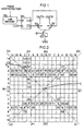
- Figure 1 is a layout of a known example of a cell with an associated decoding logic for a matrix structure of a digital-analog converter.
- Figure 2 is an example of a selecting scheme for a sequence of cells inside a bidimensional matrix structure of a digital-analog converter according to the invention.
- Figure 1 shows an example chosen among others of a cell for a bidimensional matrix structure of a digital-analog converter.
- the switching element illustrated on figure 1 comprises two mirrored transistors 01 and 02 connected in parallel and the current source comprises a third transistor 03.
- the sources of transistors 01 and 02 are connected to the drain of transistor 03, this last having its own drain connected to a substrate ground link VSS of the matrix component.
- the drains of transistors 01 and 02 are respectively to output terminals OUTN and OUTP.
- Complementary control signals CS and CS are applied to the gates of transistors 01 and 02 and a bias voltage BV is applied to the gate of transistor 03.
- the bias voltage BV is common to all cells of the matrix structure, it controls the value of the current fed by transistor 03 in the cell to which this transistor belongs.
- Control signals CS and CS are provided by a bistable trigger 04 having a data input D connected to an output of a cell decoder 05 and a clock input C receiving a clock signal CLK common for all the cells in the converter.
- the cell decoder 05 receives row and column controls from a matrix addressing logic for switching on the current source when required. As already known the matrix addressing logic when receiving a digital signal converts such a signal in row and column controls for switching on a number of current sources depending on the digital value of the received signal.
- graded and symmetrical errors originating from mismatched sources are avoided with a hierarchical symmetrical layout of the sources according to one dimension in a matrix structure. But graded and symmetrical errors remain according to the other dimension of the matrix.
- Figure 2 illustrates a method for selecting a sequence of cells inside a bidimensional matrix structure according to which such drawbacks are avoided.
- the bidimensional matrix structure is considered as assimilable at least to a rectangle or preferably to a square shared by a determined number of cells. This determined number is related to the number of sources considered as necessary for obtaining the maximal value of summed current corresponding to the highest imputable digital value for the converter, when there is one source by cell as supposed here.
- a mapping area corresponds to each cell in the bidimensional matrix structure, they are preferably identical and located side by side. Each area corresponds to a determined row and to a determined column in the matrix structure. It is assumed here that the areas correspond to identical squares, knowing that other shapes such as for instance rectangles could also be taken in account. As an example there are 255 areas for as many cells of one source illustrated on figure 2.
- An even number of areas by row and even number of areas by column are preferably chosen in the matrix structure as they provide a structure centre such as C with regard to which symmetry rules are applicable.
- Each sector is symmetrical to another sector with regard to the centre C of the structure and symmetrical to another sector with regard to every of the two mean perpendiculars M1 and M2.
- Even numbers of areas by columns and by rows in each sector are also preferably chosen and particularly with a same number for the columns and for the rows as in figure 2, but such choices are not compulsory.
- mapping areas 1, 2 for a first and a second cells of the structure, knowing that such a choice is in relation with the order for controlling the switching on of the sources, when there is only one source by cell.
- the first area 1 corresponds for instance to the cell of the first source to be switched on as soon as at least one source needs to be switched on and so on for the second and the following cells and their respective sources.
- areas 1 and 2 are both situated in a same of the four sectors defined by mean perpendiculars M1 and M2, area 1 is for instance located on a same side of symmetry point S as centre C. Alternatively, area 1 could also be selected on the other side of this symmetry point S.
- a second step there is a selection of four areas 5, 6, 7; 8 symmetrical of the four areas 1, 2, 3, 4 selected by means of the preceding first step, with regard with one of the two mean perpendicular of the matrix structure, for the four following cells, the chosen mean perpendicular being M1 on figure 2.
- a third step is then used for selecting a first of successive and yet unselected areas lined in a first area strip portion, between the first area selected and a mean perpendicular which is here mean perpendicular M2, as an area for the following cell. So is selected for instance area 9 for the ninth area, with area 9 neighbouring area 1 in the area strip portion also including areas referenced 17 and 25. Such an area is called here a primary area and is used for a further selection of a so-called secondary area for the following cell, this secondary area being chosen symmetrical of the previous primary area with regard to symmetry point S. Accordingly area 10 corresponds to a secondary area and is selected for a tenth cell. There is a further selection of a pair of areas symmetrical of a primary area and of a corresponding secondary area with regard to the centre C for the two consecutive and following cells and consequently areas 11 and 12 are selected for the eleventh and twelfth cells.
- symmetry with regard to the first mean perpendicular M1 provides the four following areas for the four consecutively following cells from the four cells selected according to the preceding third step. Accordingly areas 13 to 16 symmetrical of areas 9 to 12 with regard to mean perpendicular M1 are selected for the cells thirteen to sixteen.
- Such a repetition of the third and fourth steps is continued as a fifth step for successively each of the yet unselected areas located in the first area strip portion and accordingly for an area 25 on figure 2.
- a sixth selection step similar to the one provided from the areas of the first area strip portion, is used for a second area strip portion also included in a zone limited by the second mean perpendicular (M2) and a parallel (P1) passing through the symmetry point (S).
- this second area strip portion is a neighbour and a parallel to the first area strip portion. It is also located on the other side of the first area strip portion with regard to centre C. It comprises successive areas 33, 41, 49, 57 selected in the same way as areas 17, 25 and used as primary areas in the same way.
- a seventh step repeating the preceding step is used for every area strip portion located in parallel to the first area strip portion in the zone limited by the first mean perpendicular (M2), the parallel (P1), the mean perpendicular M1 and the edge of the structure on the same side of mean perpendicular M1 than symmetry point S, as long as remains an area strip portion in the zone with areas still unselected .
- the seventh step there is a side alternation from one area strip portion to the following one with regard to the first area strip portion.
- the area strip portion including area 65 is chosen parallel to and neighbour with first area strip portion including areas 1, 9, 17, 25 on the side of centre C.
- the following area strip portion including area 97 is chosen on the other side of first area strip portion in parallel to and neighbour with the so called second area strip portion.
- the side alternation could have been started in the other way on the inside of first area strip portion in the structure for the second area strip portion and with a further side alternation as indicated above.
- areas 1 and 2 could have been inverted with area 1 on the other side of symmetry point S with regard to centre C and consequently with an inversion for the two areas of each pair in the structure.
- Figure 2 also illustrates the row and column distribution outside of the matrix structure in relation with the control inputs for each row and column.
- mapping areas, or cells, distribution linked with the positioning of the area strip portions two rows respectively including areas 1 and 2, are neighbours of symmetry point S on each side of it and in parallel with mean perpendicular M1.
- Two columns respectively also including areas 1 and 2 are neighbours of symmetry point S on each side of it and in parallel with mean perpendicular M2.
- Rows referenced 3, 4 on figure 2 and respectively including areas 3 and 4 are respectively symmetrical to rows referenced 1 and 2 including areas 1 and 2 with regard to mean perpendicular M1. The same thing happens for the columns referenced 3, 4 including areas 3, 4 and columns referenced 1, 2 including areas 1, 2 with regard to mean perpendicular M2.
- first and second area strip portions correspond respectively to rows referenced 1, 2 and rows respectively referenced 5, 6, 9, 10 13, 14 correspond to the alternated area strip portions obtained by side alternation with regard to first area strip portion in the sector including the symmetry point S of the matrix structure.
- the consecutive cells are distributed by group of four consecutive cells, with each of the four cells of a group having an area located on a different row and on a different column with regard to the three areas corresponding to the three other cells.
- the cells included in the matrix structure are switched under control or a row decoder and of a column decoder.
- control link for each row of the matrix structure and four control links are provided for each column and the rows are activated four by four, so a very simple row decoder is required.
- the four cells sharing a same column control link are in fact in line side by side and the corresponding control link does not need to be long. If the column decoder is more complex than a column decoder with only one control link by column as in the known prior art, it is not in fact very complex.
- Such an arrangement reduces the number of conductive tracks associated to the matrix structure, simplifies the decoding arrangement required for the selection of the cells to be switched on when the converter is in use and facilitates the routing in the matrix structure, such a routing becoming very limited.
Landscapes
- Engineering & Computer Science (AREA)
- Theoretical Computer Science (AREA)
- Analogue/Digital Conversion (AREA)
Claims (3)
- Procédé de sélection d'une séquence de cellules comprenant des sources de courant à l'intérieur d'une structure matricielle de cellules d'un convertisseur numérique/analogique, où un nombre variable de sources de courant est mis en circuit en fonction de la valeur d'un signal numérique entré, et où un signal de sortie analogique correspondant est obtenu par l'addition des sorties respectives des sources qui sont mises en circuit, ladite structure dimensionnelle, considérée comme rectangulaire ou de préférence carrée, comprenant des'zones de mappage juxtaposées et identiques pour les cellules, chacune desdites zones étant attribuée à une cellule, et chaque cellule comprenant un même nombre d'au moins une source de courant, caractérisé en ce qu'il comprend les étapes suivantes :une première étape pour sélectionner deux zones voisines (1, 2) le long d'une première diagonale (D1) de la structure respectivement pour une première et une deuxième cellule de chaque côté d'un point de symétrie (S) situé à un quart de la longueur de la diagonale à partir du centre (C) de la structure rectangulaire ou carrée et une paire de zones (3, 4), respectivement symétriques de la première et de la deuxième zone par rapport au centre (C) sur la première diagonale, pour une troisième et un quatrième cellules,une deuxième étape pour sélectionner quatre zones (5 à 8) symétriques des quatre zones sélectionnées au moyen de la première étape précédente, par rapport à une première des deux perpendiculaires moyennes (M1), pour les quatre cellules suivantes,une troisième étape pour sélection une première zone parmi des zones (9, 17, 25) successives et pas encore sélectionnées, alignées dans une première portion de bande de zone entre ladite première zone (1) et l'autre perpendiculaire moyenne (M2) de la structure rectangulaire, à titre de ce qu'on appelle une zone primaire pour une sélection supplémentaire de ce qu'on appelle une zone secondaire (10) symétrique de cette zone primaire (9) par rapport au point de symétrie (S) et d'une paire de zones (11, 12) respectivement symétriques de ces zones primaire et secondaire par rapport au centre (C), la zone primaire (9) avoisinant la première zone étant sélectionnée pour la neuvième cellule, la zone secondaire (10) correspondante pour la dixième cellule et leurs zones symétriques (11, 12) respectives par rapport au centre (C) pour les onzième et douzième cellules,une quatrième étape pour sélectionner quatre zones (13 à 16) symétriques, à partir des quatre zones sélectionnées au moyen de la troisième étape précédente, par rapport à la première perpendiculaire moyenne (M1), pour les quatre cellules suivantes,une cinquième étape pour répéter les troisième et quatrième étapes pour successivement chacune des zones pas encore sélectionnées situées dans la première portion de bande de zone après la/les zone(s) primaire(s) déjà sélectionnée(s), à chaque fois pour huit cellules successives,une sixième étape pour mettre en oeuvre la cinquième étape pour chacune des zones d'une deuxième portion de bande de zone parallèle à, et voisine de la première portion de bande de zone dans une surface limitée par l'autre dite perpendiculaire moyenne (M2) et une parallèle (P1) traversant le point de symétrie (S), en liaison avec une séquence correspondante de cellules,une septième étape pour répéter la sixième étape, aussi longtemps que nécessaire, pour chaque portion de bande de zone, située dans la surface et parallèlement à la première portion de bande de zone, avec une alternance de côté d'une portion de bande de zone à la suivante, et de nouveau en liaison avec une séquence de cellules correspondante..
- Convertisseur numérique/analogique comprenant une structure matricielle bidimensionnelle de cellules, où un nombre variable de sources de courant comprises dans les cellules est mis en circuit en fonction de la valeur d'un signal numérique entré, et où un signal de sortie analogique correspondant est obtenu en additionnant les sorties respectives des sources qui sont mises en circuit, caractérisé en ce qu'il comprend des moyens de décodage de rangées et de colonnes associés, au moyen de liaisons de commande de colonnes et de rangées avec une structure matricielle de zones réparties selon la revendication 1.
- Convertisseur numérique/analogique selon la revendication 2, caractérisée en ce qu'il comprend une structure matricielle bidimensionnelle constituée de cellules avec seulement une source chacune et avec une liaison de commande pour chaque colonne (ou rangée) de cellules selon une dimension et quatre liaisons de commande pour chaque rangée (ou colonne) selon l'autre dimension de la structure matricielle.
Priority Applications (5)
| Application Number | Priority Date | Filing Date | Title |
|---|---|---|---|
| EP97402193A EP0903861B1 (fr) | 1997-09-19 | 1997-09-19 | Procédé pour la sélection d'une séquence de cellules dans une structure matricielle bidimensionale d'un convertisseur numérique-analogique et convertisseur correspondant |
| DE69721249T DE69721249T2 (de) | 1997-09-19 | 1997-09-19 | Verfahren zur Auswahl einer Zellenfolge in einer zweidimensionalen Matrixstruktur eines Digital-Analog-Wandlers und nach diesem Verfahren arbeitender Wandler |
| AT97402193T ATE238631T1 (de) | 1997-09-19 | 1997-09-19 | Verfahren zur auswahl einer zellenfolge in einer zweidimensionalen matrixstruktur eines digital- analog-wandlers und nach diesem verfahren arbeitender wandler |
| JP10258305A JPH11145834A (ja) | 1997-09-19 | 1998-09-11 | ディジタル−アナログ変換器の二次元マトリクス構造内部のセル列を選択する方法及び対応の変換器 |
| US09/153,983 US6157333A (en) | 1997-09-19 | 1998-09-16 | Method for selecting a sequence of cells inside a bidimensional matrix structure of a digital-analog converter and corresponding converter |
Applications Claiming Priority (1)
| Application Number | Priority Date | Filing Date | Title |
|---|---|---|---|
| EP97402193A EP0903861B1 (fr) | 1997-09-19 | 1997-09-19 | Procédé pour la sélection d'une séquence de cellules dans une structure matricielle bidimensionale d'un convertisseur numérique-analogique et convertisseur correspondant |
Publications (2)
| Publication Number | Publication Date |
|---|---|
| EP0903861A1 EP0903861A1 (fr) | 1999-03-24 |
| EP0903861B1 true EP0903861B1 (fr) | 2003-04-23 |
Family
ID=8229852
Family Applications (1)
| Application Number | Title | Priority Date | Filing Date |
|---|---|---|---|
| EP97402193A Expired - Lifetime EP0903861B1 (fr) | 1997-09-19 | 1997-09-19 | Procédé pour la sélection d'une séquence de cellules dans une structure matricielle bidimensionale d'un convertisseur numérique-analogique et convertisseur correspondant |
Country Status (5)
| Country | Link |
|---|---|
| US (1) | US6157333A (fr) |
| EP (1) | EP0903861B1 (fr) |
| JP (1) | JPH11145834A (fr) |
| AT (1) | ATE238631T1 (fr) |
| DE (1) | DE69721249T2 (fr) |
Families Citing this family (11)
| Publication number | Priority date | Publication date | Assignee | Title |
|---|---|---|---|---|
| US6191719B1 (en) * | 1997-08-25 | 2001-02-20 | Broadcom Corporation | Digital to analog converter with reduced ringing |
| GB2368209B (en) * | 1998-01-08 | 2002-06-12 | Fujitsu Ltd | Cell array circuitry |
| WO2004006165A1 (fr) | 2002-07-09 | 2004-01-15 | Bnc Ip Switzerland Gmbh | Systeme et procede permettant d'obtenir des solutions d'identification securisees |
| US7084800B2 (en) * | 2003-08-19 | 2006-08-01 | Broadcom Corporation | System and method for shuffling mapping sequences |
| US7038607B2 (en) * | 2003-08-19 | 2006-05-02 | Broadcom Corporation | Modulation circuit having improved performance in the audio band |
| JP4526338B2 (ja) * | 2003-09-30 | 2010-08-18 | ローム株式会社 | D/a変換回路、有機el駆動回路および有機el表示装置 |
| US7593483B2 (en) * | 2004-05-07 | 2009-09-22 | Broadcom Corporation | Nonlinear mapping in digital-to-analog and analog-to-digital converters |
| TW200807890A (en) * | 2006-07-21 | 2008-02-01 | Beyond Innovation Tech Co Ltd | Electronic apparatus for current source array and layout method thereof |
| CN103929180B (zh) * | 2013-01-14 | 2017-04-26 | 华为技术有限公司 | 一种数模转换器以及数模转换器中电流源阵列的控制方法 |
| US9197236B1 (en) * | 2014-11-14 | 2015-11-24 | Tektronix, Inc. | Digitizer auto aperture with trigger spacing |
| WO2017048876A1 (fr) | 2015-09-14 | 2017-03-23 | Neology, Inc. | Dispositif de diagnostic embarqué (obd) pour véhicule |
Family Cites Families (7)
| Publication number | Priority date | Publication date | Assignee | Title |
|---|---|---|---|---|
| US3995304A (en) * | 1972-01-10 | 1976-11-30 | Teledyne, Inc. | D/A bit switch |
| US4658240A (en) * | 1984-05-07 | 1987-04-14 | Brooktree Corporation | Apparatus for converting data between analog and digital values |
| JPS61240716A (ja) * | 1985-04-17 | 1986-10-27 | Mitsubishi Electric Corp | ディジタルアナログコンバ−タ |
| US4859930A (en) * | 1988-02-16 | 1989-08-22 | Schouwenaars Hendrikus J | Current source arrangement |
| JP2597712B2 (ja) * | 1989-05-22 | 1997-04-09 | 株式会社東芝 | ディジタル・アナログ変換器 |
| JPH05259915A (ja) * | 1992-03-13 | 1993-10-08 | Matsushita Electric Ind Co Ltd | 電流加算型d/a変換器 |
| US5977897A (en) * | 1996-12-31 | 1999-11-02 | Lucent Technologies Inc. | Resistor string with equal resistance resistors and converter incorporating the same |
-
1997
- 1997-09-19 EP EP97402193A patent/EP0903861B1/fr not_active Expired - Lifetime
- 1997-09-19 DE DE69721249T patent/DE69721249T2/de not_active Expired - Lifetime
- 1997-09-19 AT AT97402193T patent/ATE238631T1/de not_active IP Right Cessation
-
1998
- 1998-09-11 JP JP10258305A patent/JPH11145834A/ja active Pending
- 1998-09-16 US US09/153,983 patent/US6157333A/en not_active Expired - Lifetime
Also Published As
| Publication number | Publication date |
|---|---|
| US6157333A (en) | 2000-12-05 |
| ATE238631T1 (de) | 2003-05-15 |
| JPH11145834A (ja) | 1999-05-28 |
| EP0903861A1 (fr) | 1999-03-24 |
| DE69721249D1 (de) | 2003-05-28 |
| DE69721249T2 (de) | 2004-01-29 |
Similar Documents
| Publication | Publication Date | Title |
|---|---|---|
| KR100530890B1 (ko) | 향상된선형성을가진커런트셀매트릭스를포함하는디지털-아날로그컨버터및관련방법. | |
| EP0903861B1 (fr) | Procédé pour la sélection d'une séquence de cellules dans une structure matricielle bidimensionale d'un convertisseur numérique-analogique et convertisseur correspondant | |
| US5568145A (en) | MOS current source layout technique to minimize deviation | |
| US7982644B2 (en) | D/A converter and semiconductor integrated circuit including the same | |
| US4667178A (en) | Digital to analog converter | |
| US20020036580A1 (en) | Capacitor-array D/A converter including a thermometer decoder and a capacitor array | |
| KR100209866B1 (ko) | 마스터슬라이스형의 집적 반도체 회로 | |
| KR20030021138A (ko) | A/d 변환기 | |
| US5894281A (en) | Digital-to-analog converter utilizing MOS transistor switching circuit with accompanying dummy gates to set same effective gate capacitance | |
| US4864215A (en) | Current source arrangement | |
| SE507892C2 (sv) | Förfarande och anordning för att åstadkomma en konstruktion för digital-till-analogomvandling med hög prestanda | |
| EP0713617A1 (fr) | Convertisseur n/a a circuit de commutation differentielle symetrique | |
| JPH0795089A (ja) | エンコーダー及びa/dコンバーター | |
| US6507272B1 (en) | Enhanced linearity, low switching perturbation resistor string matrices | |
| US6160507A (en) | Current bit cell and switched current network formed of such cells | |
| JPH04358418A (ja) | 多チャンネルd/a変換器 | |
| US5453743A (en) | Two-dimensional symmetric thermometer matrix decoder of digital/analog converter | |
| US7420495B2 (en) | Current source cell arrangement and digital-to-analog converter | |
| CN112448720A (zh) | 一种带刷新开关的电流舵型数模转换器 | |
| US7068978B2 (en) | Current cell type digital-to-analog converter | |
| US6304240B1 (en) | Drive circuit for liquid crystal display apparatus | |
| US6483131B1 (en) | High density and high speed cell array architecture | |
| EP0808023B1 (fr) | Cellule de bit de courant et réseau à courant commuté formé de telles cellules | |
| JPH08273362A (ja) | 半導体記憶装置 | |
| JPS61270919A (ja) | 並列型a/d変換器 |
Legal Events
| Date | Code | Title | Description |
|---|---|---|---|
| PUAI | Public reference made under article 153(3) epc to a published international application that has entered the european phase |
Free format text: ORIGINAL CODE: 0009012 |
|
| AK | Designated contracting states |
Kind code of ref document: A1 Designated state(s): AT BE DE ES FR GB IE IT NL SE |
|
| RAP3 | Party data changed (applicant data changed or rights of an application transferred) |
Owner name: ALCATEL |
|
| 17P | Request for examination filed |
Effective date: 19990924 |
|
| AKX | Designation fees paid |
Free format text: AT BE DE ES FR GB IE IT NL SE |
|
| GRAH | Despatch of communication of intention to grant a patent |
Free format text: ORIGINAL CODE: EPIDOS IGRA |
|
| GRAH | Despatch of communication of intention to grant a patent |
Free format text: ORIGINAL CODE: EPIDOS IGRA |
|
| GRAA | (expected) grant |
Free format text: ORIGINAL CODE: 0009210 |
|
| AK | Designated contracting states |
Designated state(s): AT BE DE ES FR GB IE IT NL SE |
|
| PG25 | Lapsed in a contracting state [announced via postgrant information from national office to epo] |
Ref country code: NL Free format text: LAPSE BECAUSE OF FAILURE TO SUBMIT A TRANSLATION OF THE DESCRIPTION OR TO PAY THE FEE WITHIN THE PRESCRIBED TIME-LIMIT Effective date: 20030423 Ref country code: BE Free format text: LAPSE BECAUSE OF FAILURE TO SUBMIT A TRANSLATION OF THE DESCRIPTION OR TO PAY THE FEE WITHIN THE PRESCRIBED TIME-LIMIT Effective date: 20030423 Ref country code: AT Free format text: LAPSE BECAUSE OF FAILURE TO SUBMIT A TRANSLATION OF THE DESCRIPTION OR TO PAY THE FEE WITHIN THE PRESCRIBED TIME-LIMIT Effective date: 20030423 |
|
| REG | Reference to a national code |
Ref country code: GB Ref legal event code: FG4D |
|
| REF | Corresponds to: |
Ref document number: 69721249 Country of ref document: DE Date of ref document: 20030528 Kind code of ref document: P |
|
| REG | Reference to a national code |
Ref country code: IE Ref legal event code: FG4D |
|
| PG25 | Lapsed in a contracting state [announced via postgrant information from national office to epo] |
Ref country code: SE Free format text: LAPSE BECAUSE OF FAILURE TO SUBMIT A TRANSLATION OF THE DESCRIPTION OR TO PAY THE FEE WITHIN THE PRESCRIBED TIME-LIMIT Effective date: 20030723 |
|
| PG25 | Lapsed in a contracting state [announced via postgrant information from national office to epo] |
Ref country code: IE Free format text: LAPSE BECAUSE OF NON-PAYMENT OF DUE FEES Effective date: 20030919 |
|
| NLV1 | Nl: lapsed or annulled due to failure to fulfill the requirements of art. 29p and 29m of the patents act | ||
| PG25 | Lapsed in a contracting state [announced via postgrant information from national office to epo] |
Ref country code: ES Free format text: LAPSE BECAUSE OF FAILURE TO SUBMIT A TRANSLATION OF THE DESCRIPTION OR TO PAY THE FEE WITHIN THE PRESCRIBED TIME-LIMIT Effective date: 20031030 |
|
| ET | Fr: translation filed | ||
| PLBE | No opposition filed within time limit |
Free format text: ORIGINAL CODE: 0009261 |
|
| STAA | Information on the status of an ep patent application or granted ep patent |
Free format text: STATUS: NO OPPOSITION FILED WITHIN TIME LIMIT |
|
| 26N | No opposition filed |
Effective date: 20040126 |
|
| REG | Reference to a national code |
Ref country code: IE Ref legal event code: MM4A |
|
| REG | Reference to a national code |
Ref country code: FR Ref legal event code: GC Effective date: 20140717 |
|
| REG | Reference to a national code |
Ref country code: FR Ref legal event code: RG Effective date: 20141016 |
|
| REG | Reference to a national code |
Ref country code: FR Ref legal event code: PLFP Year of fee payment: 19 |
|
| PGFP | Annual fee paid to national office [announced via postgrant information from national office to epo] |
Ref country code: GB Payment date: 20150917 Year of fee payment: 19 Ref country code: DE Payment date: 20150922 Year of fee payment: 19 |
|
| PGFP | Annual fee paid to national office [announced via postgrant information from national office to epo] |
Ref country code: FR Payment date: 20150922 Year of fee payment: 19 |
|
| PGFP | Annual fee paid to national office [announced via postgrant information from national office to epo] |
Ref country code: IT Payment date: 20150924 Year of fee payment: 19 |
|
| REG | Reference to a national code |
Ref country code: DE Ref legal event code: R119 Ref document number: 69721249 Country of ref document: DE |
|
| GBPC | Gb: european patent ceased through non-payment of renewal fee |
Effective date: 20160919 |
|
| REG | Reference to a national code |
Ref country code: FR Ref legal event code: ST Effective date: 20170531 |
|
| PG25 | Lapsed in a contracting state [announced via postgrant information from national office to epo] |
Ref country code: DE Free format text: LAPSE BECAUSE OF NON-PAYMENT OF DUE FEES Effective date: 20170401 Ref country code: GB Free format text: LAPSE BECAUSE OF NON-PAYMENT OF DUE FEES Effective date: 20160919 Ref country code: FR Free format text: LAPSE BECAUSE OF NON-PAYMENT OF DUE FEES Effective date: 20160930 |
|
| PG25 | Lapsed in a contracting state [announced via postgrant information from national office to epo] |
Ref country code: IT Free format text: LAPSE BECAUSE OF NON-PAYMENT OF DUE FEES Effective date: 20160919 |