EP0903850A2 - Atténuateur variable en forme de Pi comportant une dynamique d'atténuation large et circuit de contrÔle applicable - Google Patents
Atténuateur variable en forme de Pi comportant une dynamique d'atténuation large et circuit de contrÔle applicable Download PDFInfo
- Publication number
- EP0903850A2 EP0903850A2 EP98440210A EP98440210A EP0903850A2 EP 0903850 A2 EP0903850 A2 EP 0903850A2 EP 98440210 A EP98440210 A EP 98440210A EP 98440210 A EP98440210 A EP 98440210A EP 0903850 A2 EP0903850 A2 EP 0903850A2
- Authority
- EP
- European Patent Office
- Prior art keywords
- series
- bias
- pin diode
- parallel
- current
- Prior art date
- Legal status (The legal status is an assumption and is not a legal conclusion. Google has not performed a legal analysis and makes no representation as to the accuracy of the status listed.)
- Withdrawn
Links
- 239000008186 active pharmaceutical agent Substances 0.000 claims abstract description 26
- 238000005516 engineering process Methods 0.000 claims description 3
- 230000008859 change Effects 0.000 description 4
- 238000003780 insertion Methods 0.000 description 4
- 230000037431 insertion Effects 0.000 description 4
- 230000008901 benefit Effects 0.000 description 3
- 239000000758 substrate Substances 0.000 description 3
- 239000000919 ceramic Substances 0.000 description 2
- 238000010276 construction Methods 0.000 description 1
- 230000001419 dependent effect Effects 0.000 description 1
- 230000003993 interaction Effects 0.000 description 1
- 238000002955 isolation Methods 0.000 description 1
- 230000004048 modification Effects 0.000 description 1
- 238000012986 modification Methods 0.000 description 1
- 230000003071 parasitic effect Effects 0.000 description 1
- 230000009467 reduction Effects 0.000 description 1
Images
Classifications
-
- H—ELECTRICITY
- H03—ELECTRONIC CIRCUITRY
- H03H—IMPEDANCE NETWORKS, e.g. RESONANT CIRCUITS; RESONATORS
- H03H7/00—Multiple-port networks comprising only passive electrical elements as network components
- H03H7/24—Frequency- independent attenuators
- H03H7/25—Frequency- independent attenuators comprising an element controlled by an electric or magnetic variable
- H03H7/253—Frequency- independent attenuators comprising an element controlled by an electric or magnetic variable the element being a diode
- H03H7/255—Frequency- independent attenuators comprising an element controlled by an electric or magnetic variable the element being a diode the element being a PIN diode
Definitions
- This invention refers to the field of controlled attenuation devices, i.e. to a variable ⁇ attenuator with wide attenuation dynamics and relevant control circuit.
- Variable ⁇ attenuators presently employed for high frequency applications such as for band 'C' (3,4 - 8,5 Ghz) application, are normally manufactured with beam-lead PIN diodes and ceramic substrates.
- band 'C' receivers an NF shaped noise in the range of 1,5 - 2 dB is presently required along with their capability of ensuring correct operation at high power ranges of about -20 dBm.
- these requirements in the known devices call for limitation of the gain of the first stage of the radio frequency amplifying chain and of the acceptable insertion losses of the subsequent attenuator, which is normally followed by a further RF amplifier. Moreover, attenuation dynamics of the variable attenuator is also dictated by said requirements.
- Typical values of the variable attenuator specifications read: Insertion losses ⁇ -2dB - attenuation dynamics > 20 dB; In/Out return loss ⁇ -10 dB, operating band > 1 Ghz.
- the present invention provides a variable ⁇ attenuator with wide attenuation dynamics and a relevant control circuit, as described better in the claims, which form integral part of this description.
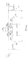
- DP1 and DP2 indicate two PIN diodes pertaining to the two parallel arms and DS a PIN diode pertaining to the series arm of the variable attenuator.
- Both the cathodes of DP2 and DS are connected together towards the radio-frequency signal input RF_IN, whereas the cathode of DP1 and the anode of DS are connected together towards the radio-frequency signal output RF_OUT.
- Applied to the anodes of DP1 and DP2 are two bias circuits consisting of a variable voltage generator Vcp generating a variable bias current Ip1 and Ip2 through respective resistances RP1 and RP2.
- a bias voltage Vdp is established across terminals of DP1 and DP2.
- CP1 and CP2 indicate two radio-frequency shortcircuit capacitances connected between the anodes of DP1 and DP2 and ground.
- CHRF1 and CHRF2 indicate two radio-frequency open-circuit inductances connected between RF_IN and ground, and between RF_OUT and node N, respectively.
- Is indicates a variable bias current of the series diode DS generated by a variable current generator Ics applied to node N and fed to the anode of DS, e.g. through CHRF2.
- a bias voltage Vds is established across the terminals of DS.
- diodes DS, DP1 and DP2 are direct current connected, if currents Ip1 and lp2 are increased, one of them tends to close at least partially on series diode DS with the increasing attenuation. For this reason Is cannot go under a certain value as it should be necessary to reach high attenuation dynamics values: therefore it is this phenomenon that limits the attenuation dynamics of the variable attenuator.
- a circuit ZB capable of subtracting a current lp3 equal to the control current Ip1 from the node N.
- the diode DP1 can be driven as if it were not grounded (balanced mode), independently from DS.
- RD1 indicates a compensating diode having its cathode connected to RP2 and its anode connected to generator Vcp. RD1 is inserted to balance the currents of the two shunt arms so as to obtain Ip1 ⁇ Ip2. Under these conditions S11 ⁇ S22. Inserted between the node N and the voltage generator Vcp is a circuit ZB through which a current Ip3 ⁇ Ip1 is flowing.
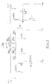
- Fig. 3 highlights a possible embodiment of the circuit ZB.
- RD2 and RD3 indicate two compensating diodes. Flowing through RD3 is a current Ics supplied through resistor R3 by the variable current generator 2lcs, which is also supplying an equal current Ics to the node N through R2.
- RD3 has its cathode grounded and its anode connected to the non inverting input of a standard operational amplifier OA, which amplifies on direct current the input voltages.
- RD2 has its cathode connected to the OA output and its anode connected to resistor RP3 also connected with the node N: a current lp3 is flowing through RD2 and RP3.
- RR1 and RR2 indicate two series connected feedback resistors: RR1 is connected between the bias voltage Vcp and the OA inverting input, whereas RR2 is connected between the latter and OA output where a voltage Vzv is established.
- bias i.e. d.c. bias
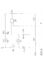
- DS and DP2 cathodes are grounded, whereas DP1 cathode and DS anode are connected with the node N.
- Ip1 Vcp - Vdp - Vds RP1
- Ip3 Vcp - Vdp - Vds RP3
- each of the three PIN diodes DS, DP1, DP2 could be connected in an opposite manner with proper modifications to the relevant bias networks evident to a person skilled in the art, and/or current Is could be passed through CHRF1.
- the problem would always be the same: there would always be a bias current of one of the two shunt arms affecting the bias current of the series arm.
- the direction of the various bias currents depends in a known manner on the insertion direction of the relevant diodes.
- a circuit like ZB is inserted in the mesh of the equivalent circuit for the bias of the PIN diode of the shunt arm affecting the bias of the series arm.
- the equivalent bias circuit of the variable attenuator object of the invention consists of three independent meshes, one for each PIN diode, so that the bias currents of both the shunt and series arms cannot flow through the series arm, but will close outside.
- variable attenuator and the relevant control circuit object of this invention have a first essential advantage of a considerable cost saving as compared with the attenuators presently in use, which consist of beam-lead PIN diodes and ceramic substrates for a whole Front-End construction in one substrate alone.
- the use of Lange-type couplers is no longer needed, whereas they are required in the known circuits to adapt both the input and output impedances of the attenuator.
- Lange couplers are highly expensive components whose usable frequency band is restricted as it is dependent on their geometrical form.
- said Lange couplers to adapt both the input and output impedances are replaced by the control of the bias currents, thus obtaining a circuit capable of operating in a very broad frequency band, only limited by the parasitic capacitances of the applied diodes.
Landscapes
- Attenuators (AREA)
- Networks Using Active Elements (AREA)
- Transmitters (AREA)
Applications Claiming Priority (2)
| Application Number | Priority Date | Filing Date | Title |
|---|---|---|---|
| ITMI972122 | 1997-09-19 | ||
| ITMI972122 IT1294752B1 (it) | 1997-09-19 | 1997-09-19 | Attenuatore variabile in configurazione pi-greca a dinamica di lavoro estesa e relativo circuito di controllo |
Publications (2)
| Publication Number | Publication Date |
|---|---|
| EP0903850A2 true EP0903850A2 (fr) | 1999-03-24 |
| EP0903850A3 EP0903850A3 (fr) | 2002-07-17 |
Family
ID=11377896
Family Applications (1)
| Application Number | Title | Priority Date | Filing Date |
|---|---|---|---|
| EP98440210A Withdrawn EP0903850A3 (fr) | 1997-09-19 | 1998-09-18 | Atténuateur variable en forme de Pi comportant une dynamique d'atténuation large et circuit de contrôle applicable |
Country Status (2)
| Country | Link |
|---|---|
| EP (1) | EP0903850A3 (fr) |
| IT (1) | IT1294752B1 (fr) |
Family Cites Families (1)
| Publication number | Priority date | Publication date | Assignee | Title |
|---|---|---|---|---|
| US4236126A (en) * | 1979-04-25 | 1980-11-25 | Cincinnati Electronics Corporation | Variable RF attenuator |
-
1997
- 1997-09-19 IT ITMI972122 patent/IT1294752B1/it active IP Right Grant
-
1998
- 1998-09-18 EP EP98440210A patent/EP0903850A3/fr not_active Withdrawn
Also Published As
| Publication number | Publication date |
|---|---|
| EP0903850A3 (fr) | 2002-07-17 |
| IT1294752B1 (it) | 1999-04-12 |
| ITMI972122A1 (it) | 1999-03-19 |
Similar Documents
| Publication | Publication Date | Title |
|---|---|---|
| FI101505B (fi) | Menetelmä suuntakytkimellä toteutetun tehonmittauksen parantamiseksi p ienillä tehotasoilla | |
| US6597242B2 (en) | Reconfigurable device for amplifying RF signals | |
| KR100480071B1 (ko) | 가변 감쇠기 | |
| US5508657A (en) | Feed forward cancellation amplifier utilizing dynamic vector control | |
| US20070069820A1 (en) | Electronic parts for high frequency power amplifier | |
| FI91928C (fi) | Menetelmä ja järjestely optisen vastaanottimen etuasteen dynamiikka-alueen kasvattamiseksi | |
| US4236126A (en) | Variable RF attenuator | |
| KR100330519B1 (ko) | 마이크로파자동이득제어장치 | |
| KR20040043306A (ko) | 도허티 증폭기를 이용한 신호 증폭 장치 | |
| US6624700B2 (en) | Radio frequency power amplifier for cellular telephones | |
| WO1999059243A1 (fr) | Circuit a semi-conducteur | |
| US5862464A (en) | Pin diode variable attenuator | |
| GB2334838A (en) | Variable rf attenuator using shunt connected antiparallel pair of bipolar transistors | |
| US6985020B2 (en) | Inline predistortion for both CSO and CTB correction | |
| KR20020094436A (ko) | 이동단말기에서 자동이득제어기의 온도보상회로 | |
| EP0903850A2 (fr) | Atténuateur variable en forme de Pi comportant une dynamique d'atténuation large et circuit de contrÔle applicable | |
| US6788149B2 (en) | Broad-band biasing system for biasing an electronic circuit and an amplifier incorporating the system | |
| US5894490A (en) | Increasing the impedance of solid state light source subsystems | |
| US5619152A (en) | Circuit arrangement for supplying an alternating signal current | |
| KR20030022104A (ko) | 안테나 증폭기 | |
| JPH1188082A (ja) | 増幅装置および携帯電話装置 | |
| KR0133541Y1 (ko) | 가변 감쇄기 | |
| US20070132512A1 (en) | Variable gain amplifier | |
| KR100263527B1 (ko) | 디지털 제어 가변 감쇠기 | |
| KR100377023B1 (ko) | 가변 감쇠기 |
Legal Events
| Date | Code | Title | Description |
|---|---|---|---|
| PUAI | Public reference made under article 153(3) epc to a published international application that has entered the european phase |
Free format text: ORIGINAL CODE: 0009012 |
|
| AK | Designated contracting states |
Kind code of ref document: A2 Designated state(s): AT BE CH CY DE DK ES FI FR GB GR IE IT LI LU MC NL PT SE |
|
| AX | Request for extension of the european patent |
Free format text: AL;LT;LV;MK;RO;SI |
|
| RAP3 | Party data changed (applicant data changed or rights of an application transferred) |
Owner name: ALCATEL |
|
| PUAL | Search report despatched |
Free format text: ORIGINAL CODE: 0009013 |
|
| AK | Designated contracting states |
Kind code of ref document: A3 Designated state(s): AT BE CH CY DE DK ES FI FR GB GR IE IT LI LU MC NL PT SE |
|
| AX | Request for extension of the european patent |
Free format text: AL;LT;LV;MK;RO;SI |
|
| AKX | Designation fees paid |
Designated state(s): DE ES FR GB IT SE |
|
| STAA | Information on the status of an ep patent application or granted ep patent |
Free format text: STATUS: THE APPLICATION IS DEEMED TO BE WITHDRAWN |
|
| 18D | Application deemed to be withdrawn |
Effective date: 20030118 |