EP0903820A2 - Laser à semi-conducteur à deux sections à réaction distribuée à couplage complexe avec accordabilité de longeur d'onde amélioré - Google Patents
Laser à semi-conducteur à deux sections à réaction distribuée à couplage complexe avec accordabilité de longeur d'onde amélioré Download PDFInfo
- Publication number
- EP0903820A2 EP0903820A2 EP98307439A EP98307439A EP0903820A2 EP 0903820 A2 EP0903820 A2 EP 0903820A2 EP 98307439 A EP98307439 A EP 98307439A EP 98307439 A EP98307439 A EP 98307439A EP 0903820 A2 EP0903820 A2 EP 0903820A2
- Authority
- EP
- European Patent Office
- Prior art keywords
- laser
- section
- pumping
- mode
- bragg
- Prior art date
- Legal status (The legal status is an assumption and is not a legal conclusion. Google has not performed a legal analysis and makes no representation as to the accuracy of the status listed.)
- Withdrawn
Links
Images


Classifications
-
- H—ELECTRICITY
- H01—ELECTRIC ELEMENTS
- H01S—DEVICES USING THE PROCESS OF LIGHT AMPLIFICATION BY STIMULATED EMISSION OF RADIATION [LASER] TO AMPLIFY OR GENERATE LIGHT; DEVICES USING STIMULATED EMISSION OF ELECTROMAGNETIC RADIATION IN WAVE RANGES OTHER THAN OPTICAL
- H01S5/00—Semiconductor lasers
- H01S5/06—Arrangements for controlling the laser output parameters, e.g. by operating on the active medium
- H01S5/062—Arrangements for controlling the laser output parameters, e.g. by operating on the active medium by varying the potential of the electrodes
- H01S5/0625—Arrangements for controlling the laser output parameters, e.g. by operating on the active medium by varying the potential of the electrodes in multi-section lasers
- H01S5/06255—Controlling the frequency of the radiation
- H01S5/06258—Controlling the frequency of the radiation with DFB-structure
-
- H—ELECTRICITY
- H01—ELECTRIC ELEMENTS
- H01S—DEVICES USING THE PROCESS OF LIGHT AMPLIFICATION BY STIMULATED EMISSION OF RADIATION [LASER] TO AMPLIFY OR GENERATE LIGHT; DEVICES USING STIMULATED EMISSION OF ELECTROMAGNETIC RADIATION IN WAVE RANGES OTHER THAN OPTICAL
- H01S5/00—Semiconductor lasers
- H01S5/10—Construction or shape of the optical resonator, e.g. extended or external cavity, coupled cavities, bent-guide, varying width, thickness or composition of the active region
- H01S5/12—Construction or shape of the optical resonator, e.g. extended or external cavity, coupled cavities, bent-guide, varying width, thickness or composition of the active region the resonator having a periodic structure, e.g. in distributed feedback [DFB] lasers
- H01S5/1228—DFB lasers with a complex coupled grating, e.g. gain or loss coupling
Definitions
- the invention relates to semiconductor lasers, and in particular, to complex coupled distributed feedback (DFB) semiconductor lasers with enhanced continuous wavelength tuning range, and methods of operating and fabricating such lasers.
- DFB distributed feedback
- Fiber optics communication systems require compact light emitting sources capable of generating single-mode, tunable, narrow linewidth radiation in the 1.3 - 1.56 ⁇ m wavelength range.
- Some of the existing semiconductor lasers for example, InGaAsP DFB lasers can meet requirements for high power and proper wavelength, but a high dynamic single mode yield is difficult to achieve.
- Conventional index coupled DFB lasers employing an index corrugation have an inherent problem in existence of two longitudinal modes with an equal threshold gain which results in poor single mode operation as shown, for example, in the article by H. Kogelnik and C.V. Shank "Coupled-mode theory of distributed feedback lasers", J. Appl. Phys.; vol. 43, no. 5, pp. 2327 - 2335, 1972.
- Previously known gain coupled or loss coupled DFB lasers utilize only one type of complex coupling which results in a high dynamic single mode yield for one of predetermined and dominant Bragg mode only.
- the random distribution of cleaved or HR-coated laser facets is usually the major reason why the opposite Bragg mode across the stop band sometimes actually lases as the dominant mode.
- SMSR side mode suppression ratio
- complex coupled lasers appear to be the best candidates for a wide range tuning.
- Complex coupled DFB lasers are preferably used as building blocks for tunable lasers to ensure a high SMSR and provide high single mode yield and a small degradation of SMSR over injection current variation. Nevertheless, the tuning range of these lasers is still limited which results in a continued demand for further increasing a tuning range of DFB lasers while maintaining other essential characteristics of the lasers, and development of effective methods of their operation.
- the present invention also seeks to provide a distributed feedback complex coupled semiconductor laser with enhanced continuous tuning range, and methods of operating and fabricating thereof.
- a distributed feedback single mode complex coupled semiconductor laser device comprising:
- a two-section semiconductor laser device using a master and slave type of pumping control is provided.
- the left Bragg mode is activated by pumping the first section above a threshold level, the second section being unpumped or pumped in reverse, a loss coupling mechanism of laser operation being provided.
- the right Bragg mode is activated by pumping the first section above a transparency level and the second section above a threshold level, a gain coupling mechanism of laser operation being provided.
- loss or gain coupling mechanisms an effective switching between two Bragg modes across a laser stop band is achieved.
- a DFB laser with enhanced tuning wavelength range is provided.
- the tuning range extends across a whole range of left and right Bragg modes.
- the active region of the laser comprises a multiple quantum well structure.
- a complex coupled grating structure comprises a uniform or chirped grating, having one or two grating sections, positionally corresponding to the first and the second sections of the laser. Two grating sections may have the same or different corrugation periods. Beneficially the grating structure is patterned by periodic etching grooves through the active region. Alternatively it may be formed in the layer adjacent to the active region by holographic exposure.
- First and second excitation means for an independent pumping of first and second sections of the laser comprises electrical contacts for current injection into the active region.
- the semiconductor laser device may be capable of coupling to an external optical pumping source to create a population inversion.
- a first and second electrode for pumping of first and second sections of the laser are formed on a top of the currant confining region of the laser.
- the current confining region is preferably a ridge waveguide or a buried hetero-structure.
- a distributed feedback single mode complex coupled semiconductor laser device comprising:
- the left Bragg mode is activated by biasing the first section of the laser above a threshold level, the second section of the laser being unbiased, biased in reverse or below a transparency level, the loss coupling mechanism of laser operation being provided.
- the right Bragg mode is activated by biasing the first section of the laser above a transparency level and the second section above a threshold level, the gain coupling mechanism of laser operation being provided.
- the grating structure has grooves whose depth is equal to or less than a thickness of the active region.
- it is a first order uniform grating.
- the grating may be a chirped grating.
- the laser is adjusted to generate light within certain wavelength ranges.
- they are 1.3 - 1.56 ⁇ m and 0.8 - 0.9 ⁇ m for InP and GaAs alloys utilized as substrate materials correspondingly.
- a distributed feedback complex coupled semiconductor laser device having a first excitation means and a second excitation means for an independent pumping of a first section and a second section of the laser axially distinct along a cavity length direction, the method comprising:
- the method comprises a step for tuning the laser wavelength around the left and the right Bragg modes correspondingly.
- Fast varying of the pumping of two sections of the laser provides fast switching between the left and the right Bragg modes. Additional periodic modulation of the left Bragg mode and the right Bragg mode when the corresponding mode is activated, and separation of them by optical filtering techniques provides two wavelength modulation at the same time.
- a method of enhancing a tuning range in a distributed feedback complex coupled semiconductor laser device having a first electrode and a second electrode for independent current injection into a first section and a second section of the laser axially distinct along a cavity length direction, the method comprising:
- a distributed feedback single mode complex coupled semiconductor laser device comprising:
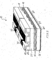
- FIG. 1 A schematic cross section through a distributed feedback single mode complex coupled laser device 10 according to a first embodiment of the present invention is shown in Figure 1.
- the device 10 comprises a substrate 12 providing a first confinement region, and active region 14 comprising a multiple quantum well structure 16 and a grating structure 18 defined therein, and an overlying confinement region 20 .
- Means for excitation of the laser device are formed thereon, and include a contact to the substrate, and a first and second current confining ridges 22 and 24 defining first and second sections 26 and 28 of the laser axially distinct along a cavity length direction, first and second contact electrodes 30 and 32 being defined on each ridge respectively for current injection into the device structure.
- the dual control electrode structure provides for operation of the first and second sections of the laser in a master and slave type control which will be described in detail below.
- a DFB semiconductor laser device 10 is fabricated from Group III-V semiconductor materials, and comprises a heavily P-doped InP substrate 12 , on which an P-doped InP buffer layer 34 of 1.5 ⁇ m thickness is defined.
- the first separate confinement region 35 consisting of four confinement layers 36, 38, 40 and 42 of P-doped InGaAsP with energy band gaps corresponding to wavelengths of 1.0 ⁇ m, 1.1 ⁇ m, 1.2 ⁇ m and 1.25 ⁇ m respectively, is provided over the buffer layer 34 .
- each confinement layer is 20 nm, and the confinement layer 36 corresponding to the 1.0 ⁇ m wavelength is adjacent to the buffer layer 34 .
- the active region 14 overlies the confinement region 35 and comprises a multiple quantum well (MQW) structure 16 which includes eight 1% compressively strained P-doped InGaAsP quantum wells 44 , each being 5 nm thick, separated by seven P-doped InGaAsP unstrained barriers 46 with a band gap corresponding to wavelength of 1.25 ⁇ m, each barrier being 10 nm thick.
- MQW multiple quantum well
- the alloy composition and layer thickness of the MQW structure 16 are tailored to have specific band gap energies to provide for lasing at a required wavelength.
- a second separate confinement region 47 consisting of two P-doped InGaAsP confinement layers 48 and 50 , having energy band gaps corresponding to 1.2 ⁇ m and 1.25 ⁇ m wavelengths respectively, is grown on top of the MQW active region 14 , each layer being 20 nm thick.
- a grating structure 18 is defined by periodically etched grooves through the active region 14 as will be described in more detail below.
- the pitch of the groove is selected so as to define a first order grating for the lasing wavelength.
- a P-doped InP layer 52 having a band gap wavelength smaller than the quantum well band gap wavelength, fills the grooves.
- a length of the first section 26 of the laser is equal to or less than a length the second section 28 of the laser, each section being reasonably long so that each of them can be viewed as an independent DFB laser, at least capable of lasing at a low threshold current in the absence of the other DFB laser attached along a laser cavity direction.
- the separation between the adjacent electrodes 30 and 32 is in the range of 5 to 15 ⁇ m to ensure both a sufficient electrical isolation between the adjacent electrodes and a limited material absorption loss.
- a bottom electrical N-contact 64 is provided at the bottom of the substrate 12 .
- Corresponding means (not shown) for controllably varying current injection and changing a temperature of each section of the laser for switching between two Bragg modes within a stop band and tuning a laser wavelength around the left Bragg mode and the right Bragg mode correspondingly are provided.
- a DFB semiconductor laser having a first section 26 and a second section 28 of the laser, axially distinct along a cavity length direction, with a first electrode 30 and a second electrode 32 for an independent current injection into the corresponding section of the laser, and the grating structure 18 under each of the electrodes is provided.
- a complimentary structure may be fabricated on a P-type wafer.
- the substrate 12 on which the laser device 10 described above is fabricated is made of InP material which results in generating a laser light within a range of 1.3-1.56 ⁇ m, corresponding to a transparency window of this material.
- the substrate may be made of GaAs material, having a window of transparency in a shorter wavelength range of 0.8-0.9 ⁇ m, which results in generating light in this wavelength range. More precise calculation of a lasing wavelength depends also on the properties of the active region and the grating structure.
- the grating period is determined by an integer multiple of ⁇ / 2n where ⁇ is very close to the desired lasing wavelength, (typically within several nm), and n is the refractive index of the material, usually in a range of 3-4 for semiconductor materials.
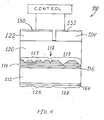
- a semiconductor laser 100 according to a second embodiment is shown in Fig. 4. It comprises a substrate 112 providing a first confinement region, an active region 114 comprising a multiple quantum well structure 116 , a grating structure 118 , comprising two sections 117 and 119 defined therein, and an overlying confinement region 120 .
- Means for excitation the laser device are formed thereon, and include a contact 164 to the substrate 112 , and first and second confining ridges 122 and 124 , defining first and second sections 126 and 128 of the laser axially distinct along a cavity length direction of the laser device 100 , first and second contact electrodes 130 and 132 being defined on each ridge respectfully for current injection into the device structure.
- Two grating sections 117 and 119 positionally correspond to the first and second sections of the laser 126 and 128 respectively.
- a small spatial separation between grating sections 117 and 119 along a direction of travel of light may be provided, usually within a range of several micrometers.
- Grating sections 117 and 119 may have the same or different uniform corrugation periods, one or both of the grating sections 117 and 119 may also be a chirped grating.
- both grating sections 117 and 119 are made by periodic etching grooves through the active region, the depth of etching being varied from etching through several top layers of the MQW only to the deep etching grooves though all layers of the MQW structure.
- Variation of the ridge width, corresponding to the grating sections 117 and 119 may also be made to produce an effective shift in the grating period.
- periods of two grating sections 117 and 119 need to differ so as to provide a predetermined center Bragg wavelength separation of the grating sections 117 and 119 , usually within a range of several nanometers to several tens of nanometers.
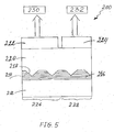
- the semiconductor laser of the embodiments described above are semiconductor diode laser structures, i.e., have contacts 30 and 32 for electrical excitation of the active region by current injection. It is also contemplated that a semiconductor laser device 200 of yet another embodiment, shown in Fig. 5, may be provided with optical pumping means 230 and 232 , replacing corresponding electrical contacts 30 and 32 of the first embodiment, e.g., by providing population inversion with suitable optical coupling to a another light source on the substrate.
- the laser 200 comprises a first excitation means 230 and a second excitation means 232 for an independent pumping of the first 226 and second 228 sections of the laser axially distinct along a cavity length direction, means for varying the pumping of the first section of the laser with respect to the pumping of the second section of the laser in a master and slave type of pumping control (not shown), and means for tuning a laser wavelength around the left and the right Bragg modes correspondingly (not shown).
- the rest of the structure of the laser device 200 is similar to that of the previous embodiments described above.
- First and second confining ridges 222 and 224 define first and second sections of the laser 226 and 228 axially distinct along a cavity length direction.
- the grating structure 218 may comprise one grating as described in the first embodiment or two section grating structure as described in the second embodiment, the grating structure 218 being uniform or chirped.
- the semiconductor laser is a ridge waveguide laser device. It is also contemplated that a semiconductor laser device in alternative embodiments may be a buried heterostructure device. A buried heterostructure laser may also comprise two section grating structure mentioned above, the grating structure being uniform or chirped.
- the active MQW region 14 will become lossy if it is not electrically pumped beyond the material transparency carrier density. The more quantum wells there are within one part of the grating period, the more optical loss the mode will experience when passing through that part of grating period.
- the active quantum wells are periodically etched away to form an in-phase gain coupling.
- the entire active MQW region 14 is left unpumped or pumped only below the transparency level, within one grating period the grating part with has higher number of quantum wells will experience higher optical loss, and that one with lower number of quantum wells will experience lower optical loss.
- the grating part that has more quantum wells has a higher refractive index, it will correspond to the longer wavelength side of stop band (right Bragg mode) . Therefore, the right Bragg mode will experience more loss than the left Bragg mode in the DFB section that are either pumped under material transparency level or left unpumped. Therefore, the underpumped section of two section complex coupled DFB laser will act as a wavelength selective filter that prefers to lase at the left Bragg mode, i.e., at the short wavelength side of the stop band.
- a master and slave type of current injection method is proposed and demonstrated in this embodiment.
- a first step only the first section 26 of the two section DFB laser 10 is biased above the threshold level while the second section 28 is left unpumped or biased in reverse.
- the small leakage current is not able to pump the second section above material transparency level. Therefore the second section 28 behaves mainly like an anti-phase loss coupled structure, which favors in lasing at the left Bragg mode as discussed above. Equivalently, the left Bragg mode from the first section 26 experiences less mirror loss than the right Bragg mode, and lases as the dominant mode.
- the bias current is increased, the wavelength can be tuned to longer wavelength by heating effect.
- the DFB laser 10 primarily behaves as a standard loss coupled DFB laser with a very high single mode yield, very stable single mode operation and excellent side mode suppression ratio (SMSR).
- SMSR side mode suppression ratio
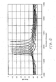
- the oscillation spectrum of the laser according to the first embodiment of the invention is shown in Fig. 6 for the first section injection current varying from 40 to 160 mA with a 20 mA step above the threshold level, the second section being unbiased, and the temperature maintained at 20 C. It is seen from Fig. 6 that the left Bragg mode lases with an excellent SMSR over the usually obtainable current or temperature tuning range.
- the first section 26 of the DFB laser serves as the master laser to provide lasing action, while the second section 28 of DFB laser serves only as a slave to provide a strong wavelength selection mechanism for the preferred left Bragg mode through a loss coupled filtering mechanism. Since only the first section 26 is biased, the laser properties are very similar to a single contact loss coupled DFB laser. That is why an excellent SMSR (over 45 dB, see Fig. 9) ratio is obtained without suffering from mode competition which takes place in conventional multi-section DFB lasers.
- the tuning range for one single contact DFB laser is limited by the possible applied current and temperature.
- a second step of laser operation is performed.
- the current injection into the first section of the laser is reduced to a level necessary to maintain the first section 26 above a transparency level only.
- the purpose of this arrangement is to provide a transparent optical path for the light generated from the second section 28 of the laser.
- the second section is then biased above the threshold level, and the injection current of second section 28 is increased from values above the threshold level to higher values for wavelength tuning. Now since both sections are biased above the material transparency level, there is no lossy part in the entire two-section DFB laser cavity.
- the first section 26 of the DFB laser serves only as slave to provide a transparent path for the light passing through, while the second section 28 of the DFB laser serves as a master laser whose lasing wavelength is tuned by current or temperature change.
- the corresponding oscillation spectrum is shown in Fig. 7 for the injection current into the first section being fixed below threshold and above a transparency level, the current injection into the second section being varied above the threshold level.
- the injection current into the first section is set at 10 mA all the time, while the current injection into the second section is increased from 40 to 160 mA with an interval of 20 mA, the temperature being maintained at 20 C.
- the combined wavelength tuning characteristics for the two-section complex coupled DFB laser according to the first embodiment of the invention are shown in Fig. 8, where tuning of both injection currents into the first and second sections of the laser produce two corresponding tuning subregions 66 and 68 .
- Two tunable subregions 66 and 68 are joined together by the stop band of the DFB laser.
- the laser starts lasing on the left Bragg mode when the injection current is low, and is gradually tuned to a longer wavelength. Normally several nanometers wavelength tuning range can be achieved by current and temperature tuning (7 nm in our experiments, as follows from the plot in Fig. 6).
- the laser starts lasing on the right Bragg mode, which wavelength is usually by several nanometers longer than that one of the left Bragg mode.
- the separation between Bragg modes is determined by the coupling strength of the DFB laser, and can be easily changed by the etching depth, grating region material composition, and laser cavity length.
- the composite two-section complex coupled DFB laser exhibits enhanced wavelength tuning range, composing of two wavelength tuning subregions, which normally sit side by side with some small overlap.
- the overlap can also be easily changed by the DFB structure and grating structure design. Therefore, the two step master and slave method of laser operation enhances a tuning range in the DFB laser, providing continuous wavelength tuning across the entire tuning range with an excellent single mode performance comparable to any stand along complex coupled DFB laser.
- the master and slave type of pumping control for controllably activating a left Bragg mode or a right Bragg mode across the laser stop band comprises the following similar steps.
- the first section of the laser is pumped above the threshold level, the second section of the laser being unpumped or pumped below a transparency level. It provides a loss coupling mechanism of laser operation, resulting in laser oscillation at the left Bragg mode.
- the first section of the laser is pumped above a transparency level, and the second section is pumped above a threshold level, the right Bragg mode being activated, and a gain coupling mechanism of laser operation being provided.
- the laser wavelength is tuned around the corresponding Bragg mode, when the mode is activated, providing extended tuning range.
- Master and slave type of laser operation control also provides fast wavelength switching between two Bragg modes. Due to reliable selection of the corresponding Bragg mode by master and slave type of current setting, fast switching of the controlling current pulse (usually within a time interval of several nanoseconds) provides fast switching between the Bragg modes, the SMSR being maintained high. Additionally, push pull current setting and periodic modulation of the left Bragg mode and the right Bragg mode, when the corresponding mode is activated, allow to form a DFB laser with two wavelength modulation. Both wavelengths are modulated at the same time by the driving signal, but with on and off status reversed. Two wavelengths are then separated by optical filters and fed into different channels of processing equipment.
- DFB lasers are dense wavelength division multiplexing systems.
- a III-V Mach-Zender (MZ) modulator (not shown) without the use of an isolator.
- MZ III-V Mach-Zender
- the MZ provides modulation at 2.488 Gb/s, and light coming out from the end of the MZ is then coupled into an optical isolator. Modulated light is transmitted through 375 km of normal nondispersion shifted fiber with an extinction 18:1.
- Fig. 10 shows the bit error rate plot (BER) as function of the received optical power for distances 0 km and 375 km (plots 74 and 76 correspondingly). No degradation is observed within the entire tuning range due to the excellent SMSR achieved during the wavelength tuning.
- BER bit error rate plot
- Fabricating of the DFB semiconductor laser device 10 according to the first embodiment shown in Fig. 1, proceeds in four stages as follows:
- the prepared substrate 12 is loaded promptly into a commercially available CVD growth chamber, and a buffer layer 14 of InP followed by the first confinement region 35, including four layers of InGaAsP, is grown.
- the active region 14 comprising eight 1% compressively strained P-doped InGaAsP quantum wells 44 , separated by seven P-doped InGaAsP unstrained barriers 46 , is grown next.
- the wafer is then removed from the growth chamber and processed so as to form photolithographically a grating structure 18 by periodically etched grooves through the active region 14 .
- a dielectric such as SiO 2 (not shown) is grown on the surface of the wafer, and the groove pattern is created in the dielectric layer.
- the grooves are etched using reactive ion etching or wet chemical etching process.
- the residual dielectric is then removed.
- an InP layer 52 is grown in the grooves.
- Etch stop layer 54 of InGaAsP grown between two buffer layers 56 and 58 of InP, followed by cladding layer 60 of InP and capping layer 62 of InGaAs complete the structure.
- a ridge mask is provided on the substrate, and the ridges are formed by etching through the capping layer 62 and top cladding layer 60 , the ridges being 2 ⁇ m nominal width.
- the split top electrodes 30 and 32 are defined by the mask used in the metalization step and created in the lift-off process.
- the front facet of the composite complex coupled DFB laser is AR-coated (anti-reflection coated).
- the back facet may be AR-coated or as-cleaved for DFB laser with a large stop band width, or HR-coated (high-reflection coated) for efficient DFB laser with a small stop band width.
- a buried heterostructure may also be grown.
- a phase mask generated by Electron Beam (EB) lithography or the direct EB writing on wafer may be used as an alternative to a wet etching process.
- the grating structure may also be formed in the layer adjacent to the active region by a holographic exposure technique.
- the structure disclosed herein is made by two step metal organic chemical vapor deposition growth and ridge waveguide processing step, and provides a significantly enhanced continuous wavelength tuning range while maintaining the excellent dynamic single mode operation inherent for the complex coupled DFB laser.
- the invention provides a complex coupled (gain coupled or loss coupled) distributed feedback (DFB) semiconductor laser, having two sections axially distinct along a cavity length direction, and two excitation means for independent pumping of corresponding sections of the laser in a master and slave type of pumping control, is provided.
- An extended continuous wavelength tuning range of the laser is obtained by selectively activating a left Bragg mode or a right Bragg mode across the stop band of the laser as a dominant lasing mode by the master and slave type of current injection control into different sections of the laser to alternate gain coupling and loss coupling mechanisms of laser operation, and further tuning a wavelength around the activated Bragg mode.
- Methods of operating the laser, enhancing a tuning range, and fabricating thereof are provided.
Landscapes
- Physics & Mathematics (AREA)
- Condensed Matter Physics & Semiconductors (AREA)
- General Physics & Mathematics (AREA)
- Electromagnetism (AREA)
- Optics & Photonics (AREA)
- Semiconductor Lasers (AREA)
Applications Claiming Priority (2)
| Application Number | Priority Date | Filing Date | Title |
|---|---|---|---|
| US933529 | 1997-09-18 | ||
| US08/933,529 US5936994A (en) | 1997-09-18 | 1997-09-18 | Two-section complex coupled distributed feedback semiconductor laser with enhanced wavelength tuning range |
Publications (2)
| Publication Number | Publication Date |
|---|---|
| EP0903820A2 true EP0903820A2 (fr) | 1999-03-24 |
| EP0903820A3 EP0903820A3 (fr) | 2000-04-26 |
Family
ID=25464132
Family Applications (1)
| Application Number | Title | Priority Date | Filing Date |
|---|---|---|---|
| EP98307439A Withdrawn EP0903820A3 (fr) | 1997-09-18 | 1998-09-14 | Laser à semi-conducteur à deux sections à réaction distribuée à couplage complexe avec accordabilité de longeur d'onde amélioré |
Country Status (3)
| Country | Link |
|---|---|
| US (1) | US5936994A (fr) |
| EP (1) | EP0903820A3 (fr) |
| JP (1) | JPH11150339A (fr) |
Cited By (3)
| Publication number | Priority date | Publication date | Assignee | Title |
|---|---|---|---|---|
| WO2001024330A1 (fr) * | 1999-09-29 | 2001-04-05 | Nortel Networks Limited | Système de laser à modulation de réflexion optique à cavité composée |
| GB2400233A (en) * | 2003-04-01 | 2004-10-06 | Agilent Technologies Inc | Distributed feedback laser device |
| WO2009036904A1 (fr) * | 2007-09-13 | 2009-03-26 | Fraunhofer-Gesellschaft zur Förderung der angewandten Forschung e.V. | Laser à semi-conducteur et procédé de fonctionnement d'un laser à semi-conducteur |
Families Citing this family (27)
| Publication number | Priority date | Publication date | Assignee | Title |
|---|---|---|---|---|
| JP3180725B2 (ja) * | 1997-08-05 | 2001-06-25 | 日本電気株式会社 | 分布帰還型半導体レーザ |
| US6104739A (en) * | 1997-12-24 | 2000-08-15 | Nortel Networks Corporation | Series of strongly complex coupled DFB lasers |
| US6650673B2 (en) * | 1998-12-15 | 2003-11-18 | Bookham Technology, Plc | Generation of short optical pulses using strongly complex coupled DFB lasers |
| US6501777B1 (en) * | 1999-01-29 | 2002-12-31 | Nec Corporation | Distributed feedback semiconductor laser emitting device having asymmetrical diffraction gratings |
| US6687278B1 (en) * | 1999-09-02 | 2004-02-03 | Agility Communications, Inc. | Method of generating an optical signal with a tunable laser source with integrated optical amplifier |
| US6909734B2 (en) * | 1999-09-02 | 2005-06-21 | Agility Communications, Inc. | High-power, manufacturable sampled grating distributed Bragg reflector lasers |
| AUPQ300199A0 (en) * | 1999-09-21 | 1999-10-14 | University Of Sydney, The | A grating design |
| EP1143582B1 (fr) * | 1999-09-29 | 2003-03-19 | The Furukawa Electric Co., Ltd. | Laser a semi-conducteur a retroaction repartie et a couplage de gain |
| US6757313B1 (en) * | 1999-11-12 | 2004-06-29 | Trumpf Photonics Inc. | Control of current spreading in semiconductor laser diodes |
| US6731663B1 (en) * | 2000-03-28 | 2004-05-04 | The Furukawa Electric Co., Ltd. | Ridge waveguide type semiconductor laser device |
| US6690693B1 (en) * | 2000-05-04 | 2004-02-10 | Agility Communications, Inc. | Power and wavelength control of sampled grating distributed Bragg reflector lasers |
| US7061943B2 (en) * | 2000-06-29 | 2006-06-13 | Agility Communications, Inc. | Controller calibration for small form factor sampled grating distributed Bragg reflector laser |
| EP1172907B1 (fr) * | 2000-07-11 | 2006-05-31 | Corning Incorporated | Amplificateur optique à gain stabilisé et adjustable |
| JP2002111135A (ja) * | 2000-10-02 | 2002-04-12 | Furukawa Electric Co Ltd:The | 半導体レーザ素子、それを用いた光ファイバ増幅器用励起光源 |
| US6954476B2 (en) * | 2001-05-15 | 2005-10-11 | Agility Communications, Inc. | Sampled grating distributed Bragg reflector laser controller |
| US6714574B2 (en) | 2001-07-31 | 2004-03-30 | Bookham Technology, Plc | Monolithically integrated optically-pumped edge-emitting semiconductor laser |
| US9372306B1 (en) | 2001-10-09 | 2016-06-21 | Infinera Corporation | Method of achieving acceptable performance in and fabrication of a monolithic photonic integrated circuit (PIC) with integrated arrays of laser sources and modulators employing an extended identical active layer (EIAL) |
| CA2363149A1 (fr) * | 2001-11-16 | 2003-05-16 | Photonami Inc. | Structures de laser dfb a emission par la surface pour systemes de communications a large bande et reseau de ces structures |
| DE10217678A1 (de) * | 2002-04-19 | 2003-11-06 | Fraunhofer Ges Forschung | Laser-Materialbearbeitung mit hybriden Prozessen |
| US10012797B1 (en) | 2002-10-08 | 2018-07-03 | Infinera Corporation | Monolithic photonic integrated circuit (PIC) with a plurality of integrated arrays of laser sources and modulators employing an extended identical active layer (EIAL) |
| KR100964399B1 (ko) * | 2003-03-08 | 2010-06-17 | 삼성전자주식회사 | 반도체 레이저 다이오드 및 이를 채용한 반도체 레이저다이오드 조립체 |
| US20050013337A1 (en) * | 2003-05-30 | 2005-01-20 | Thomas Jung | Semiconductor injection locked lasers and method |
| US7649916B2 (en) * | 2004-06-30 | 2010-01-19 | Finisar Corporation | Semiconductor laser with side mode suppression |
| JP2006019516A (ja) * | 2004-07-01 | 2006-01-19 | Fujitsu Ltd | 波長可変レーザ及びその制御方法 |
| TWI250706B (en) * | 2005-02-24 | 2006-03-01 | Gigacomm Corppration | Optical communication module and multimode distributed feedback laser diode |
| JP5633289B2 (ja) * | 2010-10-04 | 2014-12-03 | 日亜化学工業株式会社 | 半導体レーザ素子の駆動方法及び半導体レーザ装置 |
| CN121566271A (zh) * | 2026-01-23 | 2026-02-24 | 日照市艾锐光电科技有限公司 | 隔离式半导体激光器、光发射组件及光模块 |
Family Cites Families (4)
| Publication number | Priority date | Publication date | Assignee | Title |
|---|---|---|---|---|
| US5119393A (en) * | 1989-06-14 | 1992-06-02 | Hitachi, Ltd. | Semiconductor laser device capable of controlling wavelength shift |
| DE69117488T2 (de) * | 1990-10-19 | 1996-10-02 | Optical Measurement Technology | Halbleiterlaser mit verteilter rückkoppelung |
| SE502625C2 (sv) * | 1993-09-02 | 1995-11-27 | Ellemtel Utvecklings Ab | Avstämbar förstärkningskopplad laseranordning |
| US6104739A (en) * | 1997-12-24 | 2000-08-15 | Nortel Networks Corporation | Series of strongly complex coupled DFB lasers |
-
1997
- 1997-09-18 US US08/933,529 patent/US5936994A/en not_active Expired - Fee Related
-
1998
- 1998-09-14 EP EP98307439A patent/EP0903820A3/fr not_active Withdrawn
- 1998-09-18 JP JP10264323A patent/JPH11150339A/ja active Pending
Cited By (7)
| Publication number | Priority date | Publication date | Assignee | Title |
|---|---|---|---|---|
| WO2001024330A1 (fr) * | 1999-09-29 | 2001-04-05 | Nortel Networks Limited | Système de laser à modulation de réflexion optique à cavité composée |
| US6519270B1 (en) | 1999-09-29 | 2003-02-11 | Bookham Technology Plc | Compound cavity reflection modulation laser system |
| GB2400233A (en) * | 2003-04-01 | 2004-10-06 | Agilent Technologies Inc | Distributed feedback laser device |
| GB2400233B (en) * | 2003-04-01 | 2006-05-10 | Agilent Technologies Inc | Distributed feedback laser device |
| WO2009036904A1 (fr) * | 2007-09-13 | 2009-03-26 | Fraunhofer-Gesellschaft zur Förderung der angewandten Forschung e.V. | Laser à semi-conducteur et procédé de fonctionnement d'un laser à semi-conducteur |
| DE102007044848A1 (de) * | 2007-09-13 | 2009-04-02 | Fraunhofer-Gesellschaft zur Förderung der angewandten Forschung e.V. | Halbleiterlaser und Verfahren zum Betreiben eines Halbleiterlasers |
| DE102007044848B4 (de) * | 2007-09-13 | 2009-12-31 | Fraunhofer-Gesellschaft zur Förderung der angewandten Forschung e.V. | Halbleiterlaser und Verfahren zum Betreiben eines Halbleiterlasers |
Also Published As
| Publication number | Publication date |
|---|---|
| JPH11150339A (ja) | 1999-06-02 |
| EP0903820A3 (fr) | 2000-04-26 |
| US5936994A (en) | 1999-08-10 |
Similar Documents
| Publication | Publication Date | Title |
|---|---|---|
| US5936994A (en) | Two-section complex coupled distributed feedback semiconductor laser with enhanced wavelength tuning range | |
| US6104739A (en) | Series of strongly complex coupled DFB lasers | |
| EP0836255B1 (fr) | Réseau laser à diode et méthode de fabrication | |
| US5838714A (en) | Tunable wavelength laser emission components | |
| US5452318A (en) | Gain-coupled DFB laser with index coupling compensation | |
| US5699378A (en) | Optical comb filters used with waveguide, laser and manufacturing method of same | |
| US4873691A (en) | Wavelength-tunable semiconductor laser | |
| US6252895B1 (en) | Distributed feedback semiconductor laser in which light intensity distributions differ in different polarization modes, and driving method therefor | |
| US6026110A (en) | Distributed feedback semiconductor laser with gain modulation | |
| US6198863B1 (en) | Optical filters | |
| US20040179569A1 (en) | Wavelength tunable DBR laser diode | |
| JP4026334B2 (ja) | 半導体レーザ、分布帰還型半導体レーザおよび波長可変半導体レーザ | |
| CA2410964C (fr) | Lasers haute puissance a reflecteurs de bragg a reseaux echantillonnes | |
| EP0911927A1 (fr) | Source laser à semiconducteur accordable à bande large | |
| US20020064203A1 (en) | Strip-loaded tunable distributed feedback laser | |
| JPH07249829A (ja) | 分布帰還型半導体レーザ | |
| US6643309B1 (en) | Semiconductor laser device | |
| EP0753914B1 (fr) | Elément laser à diode à caractéristique excellente de distorsion d'intermodulation | |
| Lammert et al. | MQW wavelength-tunable DBR lasers with monolithically integrated external cavity electroabsorption modulators with low-driving voltages fabricated by selective-area MOCVD | |
| Hong et al. | Cascaded strongly gain-coupled (SGC) DFB lasers with 15-nm continuous-wavelength tuning | |
| Hong et al. | Enhanced wavelength tuning range in two-section complex-coupled DFB lasers by alternating gain and loss coupling | |
| JP2003234541A (ja) | 分布帰還型半導体レーザ素子 | |
| JP3149961B2 (ja) | 多波長半導体レーザ素子及びその駆動方法 | |
| JP2770722B2 (ja) | 波長可変半導体レーザの製造方法 | |
| WO2000036717A1 (fr) | Laser a semi-conducteur a retroaction repartie et a couplage de gain |
Legal Events
| Date | Code | Title | Description |
|---|---|---|---|
| PUAI | Public reference made under article 153(3) epc to a published international application that has entered the european phase |
Free format text: ORIGINAL CODE: 0009012 |
|
| AK | Designated contracting states |
Kind code of ref document: A2 Designated state(s): DE FR GB |
|
| AX | Request for extension of the european patent |
Free format text: AL;LT;LV;MK;RO;SI |
|
| RAP3 | Party data changed (applicant data changed or rights of an application transferred) |
Owner name: NORTEL NETWORKS CORPORATION |
|
| PUAL | Search report despatched |
Free format text: ORIGINAL CODE: 0009013 |
|
| AK | Designated contracting states |
Kind code of ref document: A3 Designated state(s): AT BE CH CY DE DK ES FI FR GB GR IE IT LI LU MC NL PT SE |
|
| AX | Request for extension of the european patent |
Free format text: AL;LT;LV;MK;RO;SI |
|
| RAP1 | Party data changed (applicant data changed or rights of an application transferred) |
Owner name: NORTEL NETWORKS LIMITED |
|
| 17P | Request for examination filed |
Effective date: 20001026 |
|
| AKX | Designation fees paid |
Free format text: DE FR GB |
|
| RAP1 | Party data changed (applicant data changed or rights of an application transferred) |
Owner name: BOOKHAM TECHNOLOGY PLC |
|
| 111Z | Information provided on other rights and legal means of execution |
Free format text: DEFRGB Effective date: 20031030 |
|
| STAA | Information on the status of an ep patent application or granted ep patent |
Free format text: STATUS: THE APPLICATION IS DEEMED TO BE WITHDRAWN |
|
| 18D | Application deemed to be withdrawn |
Effective date: 20050331 |