EP0903786A2 - Matrice de diodes électroluminescentes et procédé de fabrication - Google Patents
Matrice de diodes électroluminescentes et procédé de fabrication Download PDFInfo
- Publication number
- EP0903786A2 EP0903786A2 EP98117050A EP98117050A EP0903786A2 EP 0903786 A2 EP0903786 A2 EP 0903786A2 EP 98117050 A EP98117050 A EP 98117050A EP 98117050 A EP98117050 A EP 98117050A EP 0903786 A2 EP0903786 A2 EP 0903786A2
- Authority
- EP
- European Patent Office
- Prior art keywords
- light
- emitting diode
- perforated plate
- emitting diodes
- plate
- Prior art date
- Legal status (The legal status is an assumption and is not a legal conclusion. Google has not performed a legal analysis and makes no representation as to the accuracy of the status listed.)
- Withdrawn
Links
Images
Classifications
-
- H—ELECTRICITY
- H10—SEMICONDUCTOR DEVICES; ELECTRIC SOLID-STATE DEVICES NOT OTHERWISE PROVIDED FOR
- H10W—GENERIC PACKAGES, INTERCONNECTIONS, CONNECTORS OR OTHER CONSTRUCTIONAL DETAILS OF DEVICES COVERED BY CLASS H10
- H10W90/00—Package configurations
-
- H—ELECTRICITY
- H05—ELECTRIC TECHNIQUES NOT OTHERWISE PROVIDED FOR
- H05K—PRINTED CIRCUITS; CASINGS OR CONSTRUCTIONAL DETAILS OF ELECTRIC APPARATUS; MANUFACTURE OF ASSEMBLAGES OF ELECTRICAL COMPONENTS
- H05K3/00—Apparatus or processes for manufacturing printed circuits
- H05K3/30—Assembling printed circuits with electric components, e.g. with resistors
- H05K3/301—Assembling printed circuits with electric components, e.g. with resistors by means of a mounting structure
Definitions
- the invention relates to a light-emitting diode array with a plurality of light-emitting diodes arranged in a matrix of rows and columns, that with a housing with a dome-like top and are provided with a base plate, led out of the pins are.
- the invention further relates to a method for Production of the light-emitting diode array and use of the Light-emitting diode arrays for the illumination of a plane Surface.
- Light-emitting diode arrays of the type mentioned are for lighting purposes known. They are used with simple and cheap, in their light intensity limited light emitting diodes a relatively high Generate light intensity in which the light of the variety of Light emitting diodes is used, for example, to cover an area illuminate.
- the advantage of such light-emitting diode arrays is in that LEDs are easy to control and high Have lifespan by switching on and off is not affected. With the well-known LED arrays Lighting can be implemented without any problems if it is only the emission of a certain amount of light is important, with certain irregularities to be accepted.
- a precision lighting with a high uniformity of the Illumination fails due to the fact that the light-emitting diodes that pass through Soldering can be connected to a control board after which Soldering are not exactly aligned. It is known that Insert LEDs individually in a housing and thereby one to enable exact alignment. However, this arrangement has the disadvantage that the LEDs are only at some distance can be arranged from each other, so that a high lighting intensity is no longer available.
- the present invention is therefore based on the problem Light emitting diode array to create both a uniform Illumination as well as a high illuminance enables.
- a light-emitting diode array is used to solve this problem of the type mentioned above, characterized in that the LEDs with their base plates on a perforated mounting plate lie flat in a ring and with bulges and the connecting wires on the underside of the base plate in an associated Hole of the base plate protrude and in the matrix with a minimal distance are arranged to each other.
- the light-emitting diodes are in the light-emitting diode array according to the invention thus arranged practically without distance from each other so with their housing or base plates together. They are nevertheless aligned exactly parallel to each other in the LED array, because they are on a perforated mounting plate with their base plates lie flat in a ring.
- This arrangement offers the advantage that on the bottom regularly in the area of the connector pins present bulges that are regularly through Leaked epoxy resin occur, the flat support and Do not disturb the alignment of the LEDs using the base plates.
- the light-emitting diode array according to the invention allows precision illuminations for the first time with high uniformity. As a result it makes sense for the LED array according to the invention, that the LEDs are connected in rows to each other in series and can be controlled line by line in their brightness.
- This embodiment of the invention is particularly useful if the LED array to produce an obliquely striking Illumination of a flat surface is used in this way is that the LEDs located in each line have the same distance to the surface, the lines of LEDs with increasing distance from the surface increasingly be controlled brightly.
- the light can pass through at an oblique angle the light-emitting diode array compensates for the oblique incidence of light uniform illumination of a field on the flat surface to reach.
- Such an arrangement is particularly useful for checking a surface for the presence of Error with a dark field lighting, which is a regular oblique incidence of light with a camera observation using a Matrix camera takes place, which is essentially perpendicular to the surface stands.
- the brightness can be controlled line by line for all possible angles of attack of the LED array Illuminated surface has a uniform intensity from that of the Surface reflected radiation can be achieved.
- the alignment of the LEDs can still be stabilized be that the dome-like tops of the LEDs in holes protrude from an upper perforated plate. This creates a parallel one Alignment of the LEDs. If doing so according to a preferred Embodiment at least the surface facing the mounting plate and preferably also the inside of the holes of the top Perforated plate absorbing the radiation from the LEDs is formed, the transmission is with the upper perforated plate prevented from secondary maxima of the LEDs, so that from Light-emitting diode array only emits essentially parallel radiation because there are no parallel rays on the absorbent Hit surfaces of the top perforated plate and therefore not as reflected rays can pass through the holes. In this way it is possible to have parallel, uniform and flat surfaces Light with the light-emitting diode array according to the invention produce.
- the correct alignment of the light-emitting diode array according to the invention is used in the manufacture of the LED array ensured the use of the upper perforated plate with its
- the dome-like tops of the LEDs are aligned with holes and the light-emitting diodes with their base plates against the mounting perforated plate be pressed until the soldering process for the connection pins is finished.
- the dome-like tops of the light-emitting diodes focusing with the light of the light-emitting diodes Lenses are provided, it may be appropriate, the upper perforated plate to be left in the LED array.
- the upper perforated plate after the soldering process, so that the LED array to the top through the LED housing is formed undisturbed.
- the use of the upper perforated plate ensures correct alignment of the individual LEDs in parallel to each other, since the LEDs with the dome-like tops in the associated Center the holes in the upper perforated plate yourself.
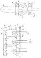
- FIG. 1 shows light-emitting diodes 1 which are used to carry out dark field illumination can preferably also be infrared diodes.
- Each light-emitting diode 1 has a conventional one that transmits the radiation Housing 2, which is from a base plate 3 in extends essentially cylindrical upwards and through a dome-like Curvature 4 is completed. Protrude through the base plate 3 down two pins 5, which for fixing the LED 1 in corresponding recordings, for example Holes 12 of a printed circuit board 13 serve. On the Bottom of the base plate 3 are regularly in the area the pins 5 protruding downward during manufacture inevitable bulges 6 caused by leaked epoxy are formed.
- the alignment of the plurality of light emitting diodes 1 parallel to one another takes place in that the light emitting diodes 1 with their base plate 3 lie on a perforated mounting plate 7, for each Light-emitting diode 1 has a through opening 8 which are dimensioned in this way is that the pins 5 through the hole 8 - and the bulges 6 can protrude into the hole 8 -, the base plate 3, however, on the edge 9 of the hole 8 in a ring-shaped area rests undisturbed by the bulges 6.
- an upper perforated plate 10 which is the same as the mounting perforated plate 7 hung up, which also has a through hole for each LED 1 11 has. Since the through hole 11 is a smaller one Diameter than the housing 2 of the LED 1, the protrudes Dome-shaped curvature 4 of the top of the LED 1 in the hole 11 and centers itself there automatically when the upper one Perforated plate 10 aligned exactly with the perforated mounting plate 7 is.
- the upper perforated plate 10 is attached so that the base plate 3 of the light-emitting diode 1 against the ring-shaped Support edge 9 of the perforated mounting plate 7 presses until the soldering process ended for the pins 5 and the LED 1 thus is permanently fixed. Then the upper perforated plate 10 be removed.
- the exact alignment of the LEDs 1 in the light-emitting diode array according to the invention allows uniform Illuminations, it being used to simplify the interconnection of the Light-emitting diodes can be useful to line these up in series switch on and controllable line by line in their brightness make each line of the LED array with a Brightness control is connected.
- Figure 2 illustrates that conventional light-emitting diodes 1 not only one have essentially axially directed luminous maximum 14 but also diagonally radiated secondary maxima 15
- the radiation the secondary maxima 15, however, is preferably by the upper Perforated plate 10 not let through.
- the surface facing the perforated mounting plate 7 14 of the upper perforated plate 10 absorbing the radiation from the LED 1 is formed.
Landscapes
- Engineering & Computer Science (AREA)
- Manufacturing & Machinery (AREA)
- Microelectronics & Electronic Packaging (AREA)
- Led Device Packages (AREA)
- Fastening Of Light Sources Or Lamp Holders (AREA)
- Formation Of Various Coating Films On Cathode Ray Tubes And Lamps (AREA)
Applications Claiming Priority (2)
| Application Number | Priority Date | Filing Date | Title |
|---|---|---|---|
| DE19741585A DE19741585C1 (de) | 1997-09-20 | 1997-09-20 | Leuchtdioden-Array, Verfahren zu seiner Herstellung und Verwendung derselben |
| DE19741585 | 1997-09-20 |
Publications (2)
| Publication Number | Publication Date |
|---|---|
| EP0903786A2 true EP0903786A2 (fr) | 1999-03-24 |
| EP0903786A3 EP0903786A3 (fr) | 2000-03-29 |
Family
ID=7843090
Family Applications (1)
| Application Number | Title | Priority Date | Filing Date |
|---|---|---|---|
| EP98117050A Withdrawn EP0903786A3 (fr) | 1997-09-20 | 1998-09-09 | Matrice de diodes électroluminescentes et procédé de fabrication |
Country Status (2)
| Country | Link |
|---|---|
| EP (1) | EP0903786A3 (fr) |
| DE (1) | DE19741585C1 (fr) |
Cited By (1)
| Publication number | Priority date | Publication date | Assignee | Title |
|---|---|---|---|---|
| US7200344B1 (en) | 2001-05-10 | 2007-04-03 | Fujitsu Limited | Receiver and method for a multichannel optical communication system |
Families Citing this family (5)
| Publication number | Priority date | Publication date | Assignee | Title |
|---|---|---|---|---|
| DE10211967B4 (de) | 2002-03-19 | 2006-08-31 | Preh Gmbh | Hinterleuchtungseinrichtung |
| US6924973B2 (en) * | 2003-04-03 | 2005-08-02 | Atto Display Co., Ltd. | Light emitting diode assembly for an illuminated sign |
| AU2003902073A0 (en) * | 2003-05-01 | 2003-05-15 | Kevin Raymond Deguara | A lighting substrate |
| DE10350472A1 (de) * | 2003-10-29 | 2005-07-07 | Carl Zeiss Jena Gmbh | Durchlichtmikroskop |
| DE102004015700A1 (de) * | 2004-03-29 | 2005-11-03 | Platsch Gmbh & Co.Kg | Flächige UV-Lichtquelle |
Family Cites Families (7)
| Publication number | Priority date | Publication date | Assignee | Title |
|---|---|---|---|---|
| CH648716A5 (de) * | 1980-07-23 | 1985-03-29 | Schurter Ag | Kombinierbares miniaturisiertes abstands- und befestigungselement fuer elektrische bauteile. |
| US4577259A (en) * | 1983-05-09 | 1986-03-18 | Motorola, Inc. | Apparatus and method for retaining an electronic device |
| JP2504533B2 (ja) * | 1988-09-02 | 1996-06-05 | 同和鉱業株式会社 | Led発光装置並びに該装置に用いる発光ブロックの製造方法 |
| JPH03171780A (ja) * | 1989-11-30 | 1991-07-25 | Toshiba Lighting & Technol Corp | 発光ダイオード表示素子 |
| GB2280534B (en) * | 1993-07-30 | 1997-04-16 | Koito Mfg Co Ltd | Display device |
| DE19528459C2 (de) * | 1995-08-03 | 2001-08-23 | Garufo Gmbh | Kühlung für ein mit LED's bestücktes Leuchtaggregat |
| US5722767A (en) * | 1996-10-22 | 1998-03-03 | Formosa Industrial Computing Inc. | LED display panel structure |
-
1997
- 1997-09-20 DE DE19741585A patent/DE19741585C1/de not_active Expired - Fee Related
-
1998
- 1998-09-09 EP EP98117050A patent/EP0903786A3/fr not_active Withdrawn
Cited By (1)
| Publication number | Priority date | Publication date | Assignee | Title |
|---|---|---|---|---|
| US7200344B1 (en) | 2001-05-10 | 2007-04-03 | Fujitsu Limited | Receiver and method for a multichannel optical communication system |
Also Published As
| Publication number | Publication date |
|---|---|
| EP0903786A3 (fr) | 2000-03-29 |
| DE19741585C1 (de) | 1998-10-01 |
Similar Documents
| Publication | Publication Date | Title |
|---|---|---|
| DE3031196C2 (de) | Beleuchteter Druckknopfschalter | |
| EP1924883B1 (fr) | Systeme de retro-eclairage comprenant des sources de lumiere a semi-conducteur disposees en groupes d'eclairage, et dispositif d'eclairage | |
| EP2070117A1 (fr) | Élément optique pour une diode lumineuse, diode lumineuse, dispositif de diodes d'émission de lumière et procédé pour la fabrication d'un dispositif de diodes d'émission de lumière | |
| DE102006002275A1 (de) | Beleuchtungseinrichtung | |
| DE2932413A1 (de) | Darstellungs- bzw. anzeigevorrichtung | |
| DE19957611A1 (de) | Beleuchtungsanordnung | |
| EP3139084A1 (fr) | Dispositif d'éclairage | |
| EP1077344A2 (fr) | Lampe | |
| EP1709359B1 (fr) | Module d'eclairage deformable | |
| EP1106913A1 (fr) | Dispositif d'affichage attachable à la surface des plaquettes de circuits | |
| DE102009020619A1 (de) | Beleuchtungsvorrichtung mit mehreren Leuchtdioden | |
| DE2731717C3 (de) | Flächiges optisches Sichtanzeigefeld | |
| DE3914448A1 (de) | Anordnung zur ausleuchtung von hintergrundflaechen | |
| DE102004004778A1 (de) | Leuchtdioden-Beleuchtungsmodul und strahlungsformende optische Einrichtung für ein Leuchtdioden-Beleuchtungsmodul | |
| WO2001059359A1 (fr) | Ensemble diode electroluminescente dote d'un reflecteur | |
| EP1098135A2 (fr) | Lampe pour véhicule | |
| DE10059844A1 (de) | Mehrfach-Warnleuchte für verschiedenfarbige Signallichter | |
| DE19741585C1 (de) | Leuchtdioden-Array, Verfahren zu seiner Herstellung und Verwendung derselben | |
| EP0905439A2 (fr) | Indicateur optique de signaux à sources lumineuses multiples | |
| DE202013010052U1 (de) | Anordnung zur Lichtabgabe sowie Leuchte mit einer solchen Anordnung | |
| DE102007009229B4 (de) | Lichtquelle zur Simulation einer Punktlichtquelle, sowie Leuchte mit einer derartigen Lichtquelle | |
| DE4100654C2 (de) | Infrarot-Scheinwerfer | |
| EP2216592B1 (fr) | Lampe | |
| DE102006001490A1 (de) | Beleuchtungseinrichtung | |
| EP3686480B1 (fr) | Agencement d'émission de lumière ayant des caractéristiques de faisceau lumineux modifiables |
Legal Events
| Date | Code | Title | Description |
|---|---|---|---|
| PUAI | Public reference made under article 153(3) epc to a published international application that has entered the european phase |
Free format text: ORIGINAL CODE: 0009012 |
|
| AK | Designated contracting states |
Kind code of ref document: A2 Designated state(s): AT BE CH CY DE DK ES FI FR GB GR IE IT LI LU MC NL PT SE |
|
| AX | Request for extension of the european patent |
Free format text: AL;LT;LV;MK;RO;SI |
|
| RAP3 | Party data changed (applicant data changed or rights of an application transferred) |
Owner name: PARSYTEC COMPUTER GMBH |
|
| PUAL | Search report despatched |
Free format text: ORIGINAL CODE: 0009013 |
|
| AK | Designated contracting states |
Kind code of ref document: A3 Designated state(s): AT BE CH CY DE DK ES FI FR GB GR IE IT LI LU MC NL PT SE |
|
| AX | Request for extension of the european patent |
Free format text: AL;LT;LV;MK;RO;SI |
|
| RIC1 | Information provided on ipc code assigned before grant |
Free format text: 7H 01L 25/13 A, 7H 01L 33/00 B, 7H 05K 3/30 B, 7G 09F 9/33 B |
|
| AKX | Designation fees paid | ||
| REG | Reference to a national code |
Ref country code: DE Ref legal event code: 8566 |
|
| STAA | Information on the status of an ep patent application or granted ep patent |
Free format text: STATUS: THE APPLICATION IS DEEMED TO BE WITHDRAWN |
|
| 18D | Application deemed to be withdrawn |
Effective date: 20020502 |