EP0903786A2 - Light emitting diode array and method of manufacturing - Google Patents
Light emitting diode array and method of manufacturing Download PDFInfo
- Publication number
- EP0903786A2 EP0903786A2 EP98117050A EP98117050A EP0903786A2 EP 0903786 A2 EP0903786 A2 EP 0903786A2 EP 98117050 A EP98117050 A EP 98117050A EP 98117050 A EP98117050 A EP 98117050A EP 0903786 A2 EP0903786 A2 EP 0903786A2
- Authority
- EP
- European Patent Office
- Prior art keywords
- light
- emitting diode
- perforated plate
- emitting diodes
- plate
- Prior art date
- Legal status (The legal status is an assumption and is not a legal conclusion. Google has not performed a legal analysis and makes no representation as to the accuracy of the status listed.)
- Withdrawn
Links
Images
Classifications
-
- H—ELECTRICITY
- H10—SEMICONDUCTOR DEVICES; ELECTRIC SOLID-STATE DEVICES NOT OTHERWISE PROVIDED FOR
- H10W—GENERIC PACKAGES, INTERCONNECTIONS, CONNECTORS OR OTHER CONSTRUCTIONAL DETAILS OF DEVICES COVERED BY CLASS H10
- H10W90/00—Package configurations
-
- H—ELECTRICITY
- H05—ELECTRIC TECHNIQUES NOT OTHERWISE PROVIDED FOR
- H05K—PRINTED CIRCUITS; CASINGS OR CONSTRUCTIONAL DETAILS OF ELECTRIC APPARATUS; MANUFACTURE OF ASSEMBLAGES OF ELECTRICAL COMPONENTS
- H05K3/00—Apparatus or processes for manufacturing printed circuits
- H05K3/30—Assembling printed circuits with electric components, e.g. with resistors
- H05K3/301—Assembling printed circuits with electric components, e.g. with resistors by means of a mounting structure
Definitions
- the invention relates to a light-emitting diode array with a plurality of light-emitting diodes arranged in a matrix of rows and columns, that with a housing with a dome-like top and are provided with a base plate, led out of the pins are.
- the invention further relates to a method for Production of the light-emitting diode array and use of the Light-emitting diode arrays for the illumination of a plane Surface.
- Light-emitting diode arrays of the type mentioned are for lighting purposes known. They are used with simple and cheap, in their light intensity limited light emitting diodes a relatively high Generate light intensity in which the light of the variety of Light emitting diodes is used, for example, to cover an area illuminate.
- the advantage of such light-emitting diode arrays is in that LEDs are easy to control and high Have lifespan by switching on and off is not affected. With the well-known LED arrays Lighting can be implemented without any problems if it is only the emission of a certain amount of light is important, with certain irregularities to be accepted.
- a precision lighting with a high uniformity of the Illumination fails due to the fact that the light-emitting diodes that pass through Soldering can be connected to a control board after which Soldering are not exactly aligned. It is known that Insert LEDs individually in a housing and thereby one to enable exact alignment. However, this arrangement has the disadvantage that the LEDs are only at some distance can be arranged from each other, so that a high lighting intensity is no longer available.
- the present invention is therefore based on the problem Light emitting diode array to create both a uniform Illumination as well as a high illuminance enables.
- a light-emitting diode array is used to solve this problem of the type mentioned above, characterized in that the LEDs with their base plates on a perforated mounting plate lie flat in a ring and with bulges and the connecting wires on the underside of the base plate in an associated Hole of the base plate protrude and in the matrix with a minimal distance are arranged to each other.
- the light-emitting diodes are in the light-emitting diode array according to the invention thus arranged practically without distance from each other so with their housing or base plates together. They are nevertheless aligned exactly parallel to each other in the LED array, because they are on a perforated mounting plate with their base plates lie flat in a ring.
- This arrangement offers the advantage that on the bottom regularly in the area of the connector pins present bulges that are regularly through Leaked epoxy resin occur, the flat support and Do not disturb the alignment of the LEDs using the base plates.
- the light-emitting diode array according to the invention allows precision illuminations for the first time with high uniformity. As a result it makes sense for the LED array according to the invention, that the LEDs are connected in rows to each other in series and can be controlled line by line in their brightness.
- This embodiment of the invention is particularly useful if the LED array to produce an obliquely striking Illumination of a flat surface is used in this way is that the LEDs located in each line have the same distance to the surface, the lines of LEDs with increasing distance from the surface increasingly be controlled brightly.
- the light can pass through at an oblique angle the light-emitting diode array compensates for the oblique incidence of light uniform illumination of a field on the flat surface to reach.
- Such an arrangement is particularly useful for checking a surface for the presence of Error with a dark field lighting, which is a regular oblique incidence of light with a camera observation using a Matrix camera takes place, which is essentially perpendicular to the surface stands.
- the brightness can be controlled line by line for all possible angles of attack of the LED array Illuminated surface has a uniform intensity from that of the Surface reflected radiation can be achieved.
- the alignment of the LEDs can still be stabilized be that the dome-like tops of the LEDs in holes protrude from an upper perforated plate. This creates a parallel one Alignment of the LEDs. If doing so according to a preferred Embodiment at least the surface facing the mounting plate and preferably also the inside of the holes of the top Perforated plate absorbing the radiation from the LEDs is formed, the transmission is with the upper perforated plate prevented from secondary maxima of the LEDs, so that from Light-emitting diode array only emits essentially parallel radiation because there are no parallel rays on the absorbent Hit surfaces of the top perforated plate and therefore not as reflected rays can pass through the holes. In this way it is possible to have parallel, uniform and flat surfaces Light with the light-emitting diode array according to the invention produce.
- the correct alignment of the light-emitting diode array according to the invention is used in the manufacture of the LED array ensured the use of the upper perforated plate with its
- the dome-like tops of the LEDs are aligned with holes and the light-emitting diodes with their base plates against the mounting perforated plate be pressed until the soldering process for the connection pins is finished.
- the dome-like tops of the light-emitting diodes focusing with the light of the light-emitting diodes Lenses are provided, it may be appropriate, the upper perforated plate to be left in the LED array.
- the upper perforated plate after the soldering process, so that the LED array to the top through the LED housing is formed undisturbed.
- the use of the upper perforated plate ensures correct alignment of the individual LEDs in parallel to each other, since the LEDs with the dome-like tops in the associated Center the holes in the upper perforated plate yourself.
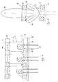
- FIG. 1 shows light-emitting diodes 1 which are used to carry out dark field illumination can preferably also be infrared diodes.
- Each light-emitting diode 1 has a conventional one that transmits the radiation Housing 2, which is from a base plate 3 in extends essentially cylindrical upwards and through a dome-like Curvature 4 is completed. Protrude through the base plate 3 down two pins 5, which for fixing the LED 1 in corresponding recordings, for example Holes 12 of a printed circuit board 13 serve. On the Bottom of the base plate 3 are regularly in the area the pins 5 protruding downward during manufacture inevitable bulges 6 caused by leaked epoxy are formed.
- the alignment of the plurality of light emitting diodes 1 parallel to one another takes place in that the light emitting diodes 1 with their base plate 3 lie on a perforated mounting plate 7, for each Light-emitting diode 1 has a through opening 8 which are dimensioned in this way is that the pins 5 through the hole 8 - and the bulges 6 can protrude into the hole 8 -, the base plate 3, however, on the edge 9 of the hole 8 in a ring-shaped area rests undisturbed by the bulges 6.
- an upper perforated plate 10 which is the same as the mounting perforated plate 7 hung up, which also has a through hole for each LED 1 11 has. Since the through hole 11 is a smaller one Diameter than the housing 2 of the LED 1, the protrudes Dome-shaped curvature 4 of the top of the LED 1 in the hole 11 and centers itself there automatically when the upper one Perforated plate 10 aligned exactly with the perforated mounting plate 7 is.
- the upper perforated plate 10 is attached so that the base plate 3 of the light-emitting diode 1 against the ring-shaped Support edge 9 of the perforated mounting plate 7 presses until the soldering process ended for the pins 5 and the LED 1 thus is permanently fixed. Then the upper perforated plate 10 be removed.
- the exact alignment of the LEDs 1 in the light-emitting diode array according to the invention allows uniform Illuminations, it being used to simplify the interconnection of the Light-emitting diodes can be useful to line these up in series switch on and controllable line by line in their brightness make each line of the LED array with a Brightness control is connected.
- Figure 2 illustrates that conventional light-emitting diodes 1 not only one have essentially axially directed luminous maximum 14 but also diagonally radiated secondary maxima 15
- the radiation the secondary maxima 15, however, is preferably by the upper Perforated plate 10 not let through.
- the surface facing the perforated mounting plate 7 14 of the upper perforated plate 10 absorbing the radiation from the LED 1 is formed.
Landscapes
- Engineering & Computer Science (AREA)
- Manufacturing & Machinery (AREA)
- Microelectronics & Electronic Packaging (AREA)
- Led Device Packages (AREA)
- Fastening Of Light Sources Or Lamp Holders (AREA)
- Formation Of Various Coating Films On Cathode Ray Tubes And Lamps (AREA)
Abstract
Description
Die Erfindung betrifft ein Leuchtdioden-Array mit einer Vielzahl von in einer Matrix aus Zeilen und Spalten angeordneten Leuchtdioden, die mit einem Gehäuse mit einer domartigen Oberseite und mit einer Basisplatte versehen sind, aus der Anschlußstifte herausgeführt sind. Die Erfindung betrifft ferner ein Verfahren zur Herstellung des Leuchtdioden-Arrays sowie eine Verwendung des Leuchtdioden-Arrays zur Erzeugung einer Beleuchtung einer ebenen Oberfläche.The invention relates to a light-emitting diode array with a plurality of light-emitting diodes arranged in a matrix of rows and columns, that with a housing with a dome-like top and are provided with a base plate, led out of the pins are. The invention further relates to a method for Production of the light-emitting diode array and use of the Light-emitting diode arrays for the illumination of a plane Surface.
Leuchtdioden-Arrays der genannten Art sind zu Beleuchtungszwecken bekannt. Sie dienen dazu, mit einfachen und billigen, in ihrer Leuchtintensität begrenzten Leuchtdioden eine relativ hohe Leuchtintensität zu erzeugen, in dem das Licht der Vielzahl von Leuchtdioden verwendet wird, beispielsweise um eine Fläche zu beleuchten. Der Vorteil derartiger Leuchtdioden-Arrays besteht darin, daß Leuchtdioden einfach steuerbar sind und eine hohe Lebensdauer aufweisen, die durch Ein- und Ausschaltvorgänge nicht beeinträchtigt wird. Mit dem bekannten Leuchtdioden-Arrays ist eine Beleuchtung dann unproblematisch realisierbar, wenn es lediglich auf die Ausstrahlung einer gewissen Lichtmenge ankommt, wobei gewisse Unregelmäßigkeiten in Kauf zu nehmen sind. Light-emitting diode arrays of the type mentioned are for lighting purposes known. They are used with simple and cheap, in their light intensity limited light emitting diodes a relatively high Generate light intensity in which the light of the variety of Light emitting diodes is used, for example, to cover an area illuminate. The advantage of such light-emitting diode arrays is in that LEDs are easy to control and high Have lifespan by switching on and off is not affected. With the well-known LED arrays Lighting can be implemented without any problems if it is only the emission of a certain amount of light is important, with certain irregularities to be accepted.
Eine Präzisionsbeleuchtung mit einer hohen Gleichmäßigkeit der Ausleuchtung scheitert daran, daß die Leuchtdioden, die durch Lötung mit einer Ansteuerungsplatine verbunden werden, nach dem Verlöten nicht exakt ausgerichtet sind. Es ist bekannt, die Leuchtdioden einzeln in ein Gehäuse einzusetzen und dadurch eine exakte Ausrichtung zu ermöglichen. Diese Anordnung hat jedoch den Nachteil, daß die Leuchtdioden dabei nur in einigem Abstand voneinander angeordnet werden können, so daß eine hohe Beleuchtungsintensität nicht mehr erreichbar ist.A precision lighting with a high uniformity of the Illumination fails due to the fact that the light-emitting diodes that pass through Soldering can be connected to a control board after which Soldering are not exactly aligned. It is known that Insert LEDs individually in a housing and thereby one to enable exact alignment. However, this arrangement has the disadvantage that the LEDs are only at some distance can be arranged from each other, so that a high lighting intensity is no longer available.
Der vorliegenden Erfindung liegt somit das Problem zugrunde, ein Leuchtdioden-Array zu erstellen, das sowohl eine gleichmäßige Ausleuchtung als auch eine hohe Beleuchtungsdichte ermöglicht.The present invention is therefore based on the problem Light emitting diode array to create both a uniform Illumination as well as a high illuminance enables.
Zur Lösung dieses Problems ist erfindungsgemäß ein Leuchtdioden-Array der eingangs erwähnten Art dadurch gekennzeichnet, daß die Leuchtdioden mit ihren Basisplatten auf einer Montage-Lochplatte ringförmig flächig aufliegen und mit Wölbungen und den Anschlußdrähten auf der Unterseite der Basisplatte in ein zugehöriges Loch der Basisplatte ragen und in der Matrix mit minimalem Abstand zueinander angeordnet sind.According to the invention, a light-emitting diode array is used to solve this problem of the type mentioned above, characterized in that the LEDs with their base plates on a perforated mounting plate lie flat in a ring and with bulges and the connecting wires on the underside of the base plate in an associated Hole of the base plate protrude and in the matrix with a minimal distance are arranged to each other.
In dem erfindungsgemäßen Leuchtdioden-Array sind die Leuchtdioden somit praktisch ohne Abstand voneinander angeordnet, stoßen also mit ihrem Gehäuse bzw. Basisplatten aneinander. Sie sind dennoch in dem Leuchtdioden-Array exakt parallel zueinander ausgerichtet, weil sie mit ihren Basisplatten auf einer Montage-Lochplatte ringförmig flächig aufliegen. Diese Anordnung bietet den Vorteil, daß die auf der Unterseite regelmäßig im Bereich der Anschlußstifte vorhandenen Wölbungen, die regelmäßig durch ausgetretenes Epoxyharz auftreten, die flächige Abstützung und Ausrichtung der Leuchtdioden mittels der Basisplatten nicht stören. Sie ragen zusammen mit den Anschlußstiften in bzw. durch das zugehörige Loch der Montage-Lochplatte, so daß die Anschlußstifte auf der Unterseite der Montage-Lochplatte mit den zugehörigen Anschlüssen, beispielsweise auf einer gedruckten Schaltungsplatine, verlötet werden und dadurch das Leuchtdioden-Array befestigt wird. Somit ist sichergestellt, daß alle Leuchtdioden den gewünschten Abstrahlwinkel beibehalten und keine durch unterschiedliche Abstrahlwinkel entstehenden Ungleichmäßigkeiten auftreten.The light-emitting diodes are in the light-emitting diode array according to the invention thus arranged practically without distance from each other so with their housing or base plates together. they are nevertheless aligned exactly parallel to each other in the LED array, because they are on a perforated mounting plate with their base plates lie flat in a ring. This arrangement offers the advantage that on the bottom regularly in the area of the connector pins present bulges that are regularly through Leaked epoxy resin occur, the flat support and Do not disturb the alignment of the LEDs using the base plates. They protrude into and through together with the connecting pins the associated hole of the mounting perforated plate, so that the connecting pins on the underside of the perforated mounting plate with the associated Connections, for example on a printed circuit board, to be soldered and thereby the LED array is attached. This ensures that all LEDs maintain the desired beam angle and none by different Irregularities resulting from the beam angle occur.
Das erfindungsgemäße Leuchtdioden-Array erlaubt erstmals Präzisionsausleuchtungen mit hoher Gleichmäßigkeit. Demzufolge kann es bei dem erfindungsgemäßen Leuchtdioden-Array sinnvoll sein, daß die Leuchtdioden zeilenweise in Serie zueinander geschaltet und zeilenweise in ihrer Helligkeit steuerbar sind.The light-emitting diode array according to the invention allows precision illuminations for the first time with high uniformity. As a result it makes sense for the LED array according to the invention, that the LEDs are connected in rows to each other in series and can be controlled line by line in their brightness.
Diese Ausführungsform der Erfindung ist besonders zweckmäßig, wenn das Leuchtdioden-Array zur Erzeugung einer schräg auffallenden Beleuchtung einer ebenen Oberfläche derart verwendet wird, daß die in jeder Zeile befindlichen Leuchtdioden einen gleichen Abstand zur Oberfläche aufweisen, wobei die Zeilen der Leuchtdioden mit zunehmenden Abstand von der Oberfläche zunehmend hell gesteuert werden.This embodiment of the invention is particularly useful if the LED array to produce an obliquely striking Illumination of a flat surface is used in this way is that the LEDs located in each line have the same distance to the surface, the lines of LEDs with increasing distance from the surface increasingly be controlled brightly.
Auf diese Weise läßt sich bei einem schrägen Lichteinfall durch das Leuchtdioden-Array eine den schrägen Lichteinfall kompensierende gleichmäßige Beleuchtung eines Feldes der ebenen Oberfläche erreichen. Eine solche Anordnung ist insbesondere zweckmäßig für die Überprüfung einer Oberfläche auf das Vorhandensein von Fehler mit einer Dunkelfeldbeleuchtung, bei der regelmäßig ein schräger Lichteinfall mit einer Kamerabeobachtung mittels einer Matrixkamera erfolgt, die im wesentlichen senkrecht zur Oberfläche steht. Durch die zeilenweise gesteuerte Helligkeit kann für alle möglichen Anstellwinkel des Leuchtdioden-Arrays zur beleuchteten Oberfläche eine gleichmäßige Intensität der von der Oberfläche reflektierten Strahlung erzielt werden.In this way, the light can pass through at an oblique angle the light-emitting diode array compensates for the oblique incidence of light uniform illumination of a field on the flat surface to reach. Such an arrangement is particularly useful for checking a surface for the presence of Error with a dark field lighting, which is a regular oblique incidence of light with a camera observation using a Matrix camera takes place, which is essentially perpendicular to the surface stands. The brightness can be controlled line by line for all possible angles of attack of the LED array Illuminated surface has a uniform intensity from that of the Surface reflected radiation can be achieved.
Die Ausrichtung der Leuchtdioden kann dadurch noch stabilisiert werden, daß die domartigen Oberseiten der Leuchtdioden in Löcher einer oberen Lochplatte ragen. Hierdurch gelingt eine parallele Ausrichtung der Leuchtdioden. Wenn dabei gemäß einer bevorzugten Ausführungsform wenigstens die zur Montageplatte zeigende Oberfläche und vorzugsweise auch die Innenseiten der Löcher der oberen Lochplatte für die Strahlung der Leuchtdioden absorbierend ausgebildet ist, wird mit der oberen Lochplatte die Aussendung von Nebenmaxima der Leuchtdioden verhindert, so daß von dem Leuchtdioden-Array nur im wesentlichen parallele Strahlung ausgesandt wird, da nicht parallele Strahlen auf die absorbierenden Flächen der oberen Lochplatte treffen und somit auch nicht als reflektierte Strahlen durch die Löcher hindurchtreten können. Auf diese Weise gelingt es, paralelles, gleichmäßiges und flächiges Licht mit dem erfindungsgemäßen Leuchtdioden-Array zu erzeugen.The alignment of the LEDs can still be stabilized be that the dome-like tops of the LEDs in holes protrude from an upper perforated plate. This creates a parallel one Alignment of the LEDs. If doing so according to a preferred Embodiment at least the surface facing the mounting plate and preferably also the inside of the holes of the top Perforated plate absorbing the radiation from the LEDs is formed, the transmission is with the upper perforated plate prevented from secondary maxima of the LEDs, so that from Light-emitting diode array only emits essentially parallel radiation because there are no parallel rays on the absorbent Hit surfaces of the top perforated plate and therefore not as reflected rays can pass through the holes. In this way it is possible to have parallel, uniform and flat surfaces Light with the light-emitting diode array according to the invention produce.
Die erfindungsgemäße korrekte Ausrichtung des Leuchtdioden-Arrays wird bei der Herstellung des Leuchtdioden-Arrays durch die Verwendung der oberen Lochplatte sichergestellt, mit deren Löchern die domartigen Oberseiten der Leuchtdioden ausgerichtet und die Leuchtdioden mit ihren Basisplatten gegen die Montage-Lochplatte gedrückt werden, bis der Lötvorgang für die Anschlußstifte beendet ist. Insbesondere wenn die domartigen Oberseiten der Leuchtdioden mit das Licht der Leuchtdioden fokussierenden Linsen versehen sind, kann es zweckmäßig sein, die obere Lochplatte im Leuchtdioden-Array zu belassen. Es ist jedoch auch möglich, die obere Lochplatte nach dem Lötvorgang zu entfernen, so daß das Leuchtdioden-Array zur Oberseite hin durch die Leuchtdiodengehäuse ungestört gebildet ist. Die Verwendung der oberen Lochplatte bewirkt einerseits die korrekte Ausrichtung der einzelnen Leuchtdioden parallel zueinander, da sich die Leuchtdioden mit den domartigen Oberseiten in den zugehörigen Löchern der oberen Lochplatte selbst zentrieren. Darüber hinaus bewirkt zusätzlich das Andrücken der unteren, flächig aufliegenden Basisplatte der Leuchtdioden auf die Montage-Lochplatte, daß die Leuchtdioden mit der zentrierten Ausrichtung und fest an der Montage-Lochplatte anliegend durch Lötung stabil fixiert werden, so daß die obere Lochplatte nach der Beendigung des Lötvorganges ohne Nachteile und ohne Gefährdung der korrekten Ausrichtung der Leuchtdioden entfernt werden kann. The correct alignment of the light-emitting diode array according to the invention is used in the manufacture of the LED array ensured the use of the upper perforated plate with its The dome-like tops of the LEDs are aligned with holes and the light-emitting diodes with their base plates against the mounting perforated plate be pressed until the soldering process for the connection pins is finished. Especially when the dome-like tops of the light-emitting diodes focusing with the light of the light-emitting diodes Lenses are provided, it may be appropriate, the upper perforated plate to be left in the LED array. However, it is also possible to remove the upper perforated plate after the soldering process, so that the LED array to the top through the LED housing is formed undisturbed. The use of the upper perforated plate ensures correct alignment of the individual LEDs in parallel to each other, since the LEDs with the dome-like tops in the associated Center the holes in the upper perforated plate yourself. Furthermore additionally causes the lower, flat support to be pressed Base plate of the LEDs on the mounting perforated plate that the light-emitting diodes with the centered alignment and firmly on the Perforated mounting plate can be firmly attached by soldering, so that the upper perforated plate after completion of the soldering process without disadvantages and without jeopardizing the correct alignment of the LEDs can be removed.
Die Erfindung soll im folgenden anhand eines in der Zeichnung dargestellten Ausführungsbeispiels näher erläutert werden. Es zeigen:
- Figur 1 -
- eine Prinzipskizze eines Ausschnitts aus einem Leuchtdioden-Array
- Figur 2 -
- eine schematisierte Darstellung der Abstrahlung einer Leuchtdiode durch eine obere Lochplatte hindurch.
- Figure 1 -
- a schematic diagram of a section of a light-emitting diode array
- Figure 2 -
- a schematic representation of the radiation of a light emitting diode through an upper perforated plate.
Figur 1 zeigt Leuchtdioden 1, die zur Durchführung einer Dunkelfeld-Beleuchtung
vorzugsweise auch Infrarotdioden sein können.
Jede Leuchtdiode 1 weist ein übliches, die Strahlung durchlassendes
Gehäuse 2 auf, das sich von einer Basisplatte 3 im
wesentlichen zylindrisch nach oben erstreckt und durch eine domartige
Wölbung 4 abgeschlossen ist. Durch die Basisplatte 3 ragen
nach unten zwei Anschlußstifte 5, die zur Fixierung der
Leuchtdiode 1 in entsprechenden Aufnahmen, beispielsweise
Löchern 12 einer gedruckten Schaltungsplatine 13 dienen. Auf der
Unterseite der Basisplatte 3 befinden sich regelmäßig im Bereich
der Anschlußstifte 5 nach unten vorstehende, bei der Fertigung
unvermeidliche Wölbungen 6, die durch ausgetretenes Epoxyharz
gebildet sind.FIG. 1 shows light-emitting diodes 1 which are used to carry out dark field illumination
can preferably also be infrared diodes.
Each light-emitting diode 1 has a conventional one that transmits the
Die Ausrichtung der Vielzahl der Leuchtdioden 1 parallel zueinander
erfolgt dadurch, daß die Leuchtdioden 1 mit ihrer Basisplatte
3 auf einer Montage-Lochplatte 7 aufliegen, die für jede
Leuchtdiode 1 eine Durchgangsöffnung 8 aufweist, die so bemessen
ist, daß die Anschlußstifte 5 durch das Loch 8 hindurch - und
die Wölbungen 6 in das Loch 8 hineinragen können -, die Basisplatte
3 jedoch auf dem Rand 9 des Loches 8 ringförmig flächig
aufliegt, und zwar ungestört durch die Wölbungen 6.The alignment of the plurality of light emitting diodes 1 parallel to one another
takes place in that the light emitting diodes 1 with their
Zur Durchführung des Lötvorganges für die Anschlußstifte 5 wird
auf die domförmige Wölbung 4 der Oberseite der Leuchtdioden 1
eine der Montage-Lochplatte 7 gleichende obere Lochplatte 10
aufgelegt, die somit für jede Leuchtdiode 1 ebenfalls ein Durchgangsloch
11 aufweist. Da das Durchgangsloch 11 einen kleineren
Durchmesser als das Gehäuse 2 der Leuchtdiode 1 hat, ragt die
domförmige Wölbung 4 der Oberseite der Leuchtdiode 1 in das Loch
11 hinein und zentriert sich dort automatisch, wenn die obere
Lochplatte 10 genau fluchtend mit der Montage-Lochplatte 7 ausgerichtet
ist. Die obere Lochplatte 10 wird so angebracht, daß
sie die Basisplatte 3 der Leuchtdiode 1 gegen den ringförmigen
Auflagerand 9 der Montage-Lochplatte 7 drückt, bis der Lötvorgang
für die Anschlußstifte 5 beendet und die Leuchtdiode 1 somit
dauerhaft fixiert ist. Danach kann die obere Lochplatte 10
entfernt werden. Die exakte Ausrichtung der Leuchtdioden 1 in
dem erfindungsgemäßen Leuchtdioden-Array erlaubt gleichmäßige
Ausleuchtungen, wobei es zur Vereinfachung der Verschaltung der
Leuchtdioden sinnvoll sein kann, diese zeilenweise in Serie zu
schalten und zeilenweise in ihrer Helligkeit steuerbar zu
machen, indem jede Zeile des Leuchtdioden-Arrays mit einer
Helligkeitssteuerung verbunden ist.To carry out the soldering process for the pins 5 is
on the dome-
Figur 2 verdeutlicht, daß übliche Leuchtdioden 1 nicht nur ein
im wesentlichen axial gerichtetes Leuchtmaximum 14 aufweisen
sondern auch schräg abgestrahlte Nebenmaxima 15. Um mit dem
Leuchtdiodenarray eine möglichst parallele Strahlung zu erreichen,
ist es zweckmäßig, nur die Strahlung in dem im wesentlichen
axialen Leuchtmaximum 14 auszunutzen, die durch die Öffnung
11 der oberen Lochplatte 10 hindurchtritt. Die Strahlung
der Nebenmaxima 15 wird hingegen vorzugsweise durch die obere
Lochplatte 10 nicht durchgelassen. Zu diesem Zweck ist es vorteilhaft,
wenn die zur Montage-Lochplatte 7 zeigende Oberfläche
14 der oberen Lochplatte 10 absorbierend für die Strahlung der
Leuchtdiode 1 ausgebildet ist.Figure 2 illustrates that conventional light-emitting diodes 1 not only one
have essentially axially directed
Claims (7)
Applications Claiming Priority (2)
| Application Number | Priority Date | Filing Date | Title |
|---|---|---|---|
| DE19741585A DE19741585C1 (en) | 1997-09-20 | 1997-09-20 | Production of light emitting diode LED matrix |
| DE19741585 | 1997-09-20 |
Publications (2)
| Publication Number | Publication Date |
|---|---|
| EP0903786A2 true EP0903786A2 (en) | 1999-03-24 |
| EP0903786A3 EP0903786A3 (en) | 2000-03-29 |
Family
ID=7843090
Family Applications (1)
| Application Number | Title | Priority Date | Filing Date |
|---|---|---|---|
| EP98117050A Withdrawn EP0903786A3 (en) | 1997-09-20 | 1998-09-09 | Light emitting diode array and method of manufacturing |
Country Status (2)
| Country | Link |
|---|---|
| EP (1) | EP0903786A3 (en) |
| DE (1) | DE19741585C1 (en) |
Cited By (1)
| Publication number | Priority date | Publication date | Assignee | Title |
|---|---|---|---|---|
| US7200344B1 (en) | 2001-05-10 | 2007-04-03 | Fujitsu Limited | Receiver and method for a multichannel optical communication system |
Families Citing this family (5)
| Publication number | Priority date | Publication date | Assignee | Title |
|---|---|---|---|---|
| DE10211967B4 (en) | 2002-03-19 | 2006-08-31 | Preh Gmbh | backlighting |
| US6924973B2 (en) * | 2003-04-03 | 2005-08-02 | Atto Display Co., Ltd. | Light emitting diode assembly for an illuminated sign |
| AU2003902073A0 (en) * | 2003-05-01 | 2003-05-15 | Kevin Raymond Deguara | A lighting substrate |
| DE10350472A1 (en) * | 2003-10-29 | 2005-07-07 | Carl Zeiss Jena Gmbh | Light microscope for dark field microscopy has aperture module which does not allow a light beam running parallel to the optical axis to pass through |
| DE102004015700A1 (en) * | 2004-03-29 | 2005-11-03 | Platsch Gmbh & Co.Kg | Flat UV light source |
Family Cites Families (7)
| Publication number | Priority date | Publication date | Assignee | Title |
|---|---|---|---|---|
| CH648716A5 (en) * | 1980-07-23 | 1985-03-29 | Schurter Ag | COMBINABLE MINIATURIZED DISTANCE AND FASTENING ELEMENT FOR ELECTRICAL COMPONENTS. |
| US4577259A (en) * | 1983-05-09 | 1986-03-18 | Motorola, Inc. | Apparatus and method for retaining an electronic device |
| JP2504533B2 (en) * | 1988-09-02 | 1996-06-05 | 同和鉱業株式会社 | LED light emitting device and method of manufacturing light emitting block used in the device |
| JPH03171780A (en) * | 1989-11-30 | 1991-07-25 | Toshiba Lighting & Technol Corp | Light emitting diode display element |
| GB2280534B (en) * | 1993-07-30 | 1997-04-16 | Koito Mfg Co Ltd | Display device |
| DE19528459C2 (en) * | 1995-08-03 | 2001-08-23 | Garufo Gmbh | Cooling for a light unit equipped with LEDs |
| US5722767A (en) * | 1996-10-22 | 1998-03-03 | Formosa Industrial Computing Inc. | LED display panel structure |
-
1997
- 1997-09-20 DE DE19741585A patent/DE19741585C1/en not_active Expired - Fee Related
-
1998
- 1998-09-09 EP EP98117050A patent/EP0903786A3/en not_active Withdrawn
Cited By (1)
| Publication number | Priority date | Publication date | Assignee | Title |
|---|---|---|---|---|
| US7200344B1 (en) | 2001-05-10 | 2007-04-03 | Fujitsu Limited | Receiver and method for a multichannel optical communication system |
Also Published As
| Publication number | Publication date |
|---|---|
| EP0903786A3 (en) | 2000-03-29 |
| DE19741585C1 (en) | 1998-10-01 |
Similar Documents
| Publication | Publication Date | Title |
|---|---|---|
| DE3031196C2 (en) | Illuminated push button switch | |
| EP1924883B1 (en) | Backlighting arrangement with semiconductor light sources arranged in light groups and lighting device | |
| EP2070117A1 (en) | Optical element for a light-emitting diode, light-emitting diode, led arrangement and method for producing an led arrangement | |
| DE102006002275A1 (en) | lighting device | |
| DE2932413A1 (en) | DISPLAY OR DISPLAY DEVICE | |
| DE19957611A1 (en) | Lighting arrangement | |
| EP3139084A1 (en) | Illumination device | |
| EP1077344A2 (en) | Lamp | |
| EP1709359B1 (en) | Deformable illumination module | |
| EP1106913A1 (en) | Circuit boards surface mountable display element | |
| DE102009020619A1 (en) | Illumination device for use as LED module in motor vehicle headlight, has optical imaging elements attached to LEDs, where imaging elements exhibit different optical imaging characteristics | |
| DE2731717C3 (en) | Flat optical display field | |
| DE3914448A1 (en) | ARRANGEMENT FOR ILLUMINATING BACKGROUND AREAS | |
| DE102004004778A1 (en) | LED lighting module for use as reading light on piece of furniture has three equispaced fluorescent plastics lenses molded in one piece with circular cover with cylindrical sides and fastening pegs | |
| WO2001059359A1 (en) | Luminous diode arrangement with a reflector | |
| EP1098135A2 (en) | Vehicle light | |
| DE10059844A1 (en) | Multiple warning light for emitting different colored signal lights has sources of different type distributed so each different colored signal light is emitted through whole transparent region | |
| DE19741585C1 (en) | Production of light emitting diode LED matrix | |
| EP0905439A2 (en) | Optical signal indicator with multiple light sources | |
| DE202013010052U1 (en) | Arrangement for emitting light and luminaire with such an arrangement | |
| DE102007009229B4 (en) | Light source for simulating a point light source, and light with such a light source | |
| DE4100654C2 (en) | Infrared headlights | |
| EP2216592B1 (en) | Lamp | |
| DE102006001490A1 (en) | lighting device | |
| EP3686480B1 (en) | Light emitting assembly with variable light emission characteristics |
Legal Events
| Date | Code | Title | Description |
|---|---|---|---|
| PUAI | Public reference made under article 153(3) epc to a published international application that has entered the european phase |
Free format text: ORIGINAL CODE: 0009012 |
|
| AK | Designated contracting states |
Kind code of ref document: A2 Designated state(s): AT BE CH CY DE DK ES FI FR GB GR IE IT LI LU MC NL PT SE |
|
| AX | Request for extension of the european patent |
Free format text: AL;LT;LV;MK;RO;SI |
|
| RAP3 | Party data changed (applicant data changed or rights of an application transferred) |
Owner name: PARSYTEC COMPUTER GMBH |
|
| PUAL | Search report despatched |
Free format text: ORIGINAL CODE: 0009013 |
|
| AK | Designated contracting states |
Kind code of ref document: A3 Designated state(s): AT BE CH CY DE DK ES FI FR GB GR IE IT LI LU MC NL PT SE |
|
| AX | Request for extension of the european patent |
Free format text: AL;LT;LV;MK;RO;SI |
|
| RIC1 | Information provided on ipc code assigned before grant |
Free format text: 7H 01L 25/13 A, 7H 01L 33/00 B, 7H 05K 3/30 B, 7G 09F 9/33 B |
|
| AKX | Designation fees paid | ||
| REG | Reference to a national code |
Ref country code: DE Ref legal event code: 8566 |
|
| STAA | Information on the status of an ep patent application or granted ep patent |
Free format text: STATUS: THE APPLICATION IS DEEMED TO BE WITHDRAWN |
|
| 18D | Application deemed to be withdrawn |
Effective date: 20020502 |