EP0903022B1 - Summierung von zittern verhinderndes digitales nachrichtenübertragungssystem - Google Patents
Summierung von zittern verhinderndes digitales nachrichtenübertragungssystem Download PDFInfo
- Publication number
- EP0903022B1 EP0903022B1 EP97926788A EP97926788A EP0903022B1 EP 0903022 B1 EP0903022 B1 EP 0903022B1 EP 97926788 A EP97926788 A EP 97926788A EP 97926788 A EP97926788 A EP 97926788A EP 0903022 B1 EP0903022 B1 EP 0903022B1
- Authority
- EP
- European Patent Office
- Prior art keywords
- bits
- input
- output
- receiver
- transmitter
- Prior art date
- Legal status (The legal status is an assumption and is not a legal conclusion. Google has not performed a legal analysis and makes no representation as to the accuracy of the status listed.)
- Expired - Lifetime
Links
Images


Classifications
-
- H—ELECTRICITY
- H04—ELECTRIC COMMUNICATION TECHNIQUE
- H04J—MULTIPLEX COMMUNICATION
- H04J3/00—Time-division multiplex systems
- H04J3/02—Details
- H04J3/06—Synchronising arrangements
- H04J3/07—Synchronising arrangements using pulse stuffing for systems with different or fluctuating information rates or bit rates
Definitions
- This invention relates to digital communication systems; and more particularly, it relates to digital communication systems which operate at bit rates which are so high that even small amounts of cumulative jitter will cause reception errors.
- One typical prior art digital communication system to which the present invention relates includes a transmitter, multiple repeaters, and a receiver; all of which are serially coupled to each other by communication channels.
- a continuous series of data bits is passed from the transmitter through each of the repeaters to the receiver.
- the transmitter, the repeaters, and the receiver each includes a respective phase-locked oscillator which locks onto the incoming series of bits, and thereby generates clock signals that determine the time instants at which the incoming bits are regenerated on an output terminal.
- jitter a problem with such a prior art digital communication system is that the timing for the serial data streams within the system deviates in an uncontrolled fashion from the ideal. These uncontrolled deviations from the ideal timing are herein referred to as "jitter". This jitter can arise from a number of factors, such as: variations in power supply voltages, variations in circuit operating temperatures, noise in 'the communication channels, the inability of the phase-locked oscillator to perfectly track and perfectly lock onto an input series of bits; etc.
- the jitter problem becomes worse as the number of repeaters between the transmitter and the receiver increases because any jitter that is within the bandwidth of a phase-locked oscillator accumulates from one repeater to the next repeater.
- the input series of bits to the first repeater has a slight amount of jitter due to any source of jitter in the transmitter, then the output series of bits will have a larger amount of jitter; the output series of bits from the second repeater will have an even larger amount of jitter; etc.
- This cumulative jitter presents a serious problem for the receiver because as it increases, the error rate which occurs in the data that is received by the receiver also increases.
- the error rate that is caused by any fixed amount of jitter also increases.
- This increase in error rate occurs because as the bit rate gets faster, the time period of each bit gets shorter; and consequently, the amount of time by which clock signals from a phase-locked oscillator can vary and still be in proper synchronization with the incoming bits gets smaller.
- the time per bit is only one billionth of a second; and thus, the amount of high frequency jitter which can be tolerated before errors will occur is just a fraction of one-billionth of a second.
- Jitter is often expressed in terms of having a particular amplitude at a particular frequency, where the amplitude is given as a multiple of one bit period at a certain nominal bit rate and the frequency is an oscillation frequency about that bit rate.
- jitter in a 100 mega-bit-per-second system can be expressed as having an amplitude of 1.5 UI pp at 6.5 KHz, where 1.5 UI pp is (1.5)x(10 nanoseconds) and 6.5 KHz is an oscillation frequency about 100 mega-bits-per-second.
- This same amount of jitter in a 1000 mega-bit-per-second system is 15 UI pp at 6.5 KHz.
- the jitter of 1.5 UI pp may be acceptable; whereas, in the 1000 Mbps system, the jitter of 15 UI pp may be totally unacceptable even though its absolute amplitude is unchanged.
- a memory 18 is. required which must have two separate inputs and two separate outputs that operate in parallel.
- One output carries a data signal DX and the other output carries a frame maker FMX as shown in Fig. 3.
- This requirement of two parallel inputs and outputs on the memory 18 occurs because without the frame marker output FMX occurring in parallel with the data output DX, a stuffing control block 28 which changes the stuffing control field SC simply will not- work. See Figs. 3 and 6 which both show that the signals DX and FMX are sent in parallel from the memory 18 through a pipeline 24 to the stuffing control block 28.
- the circuits that are recited include a memory through which two signals cannot be sent in parallel because each memory is a single-input single-output memory.
- an elastic store memory 18 in Fig. 5 stores variable length fields from an input terminal, and these fields are modified by a digital logic circuit which follows the memory.
- the primary object of the present invention is to provide a novel digital communication system in which the above problem is overcome.
- a digital communication system which includes a novel transmitter, multiple novel repeaters, and a novel receiver; all of which are serially intercoupled to each other.
- One embodiment of the novel transmitter includes an input terminal on which a continuous input series of data bits is received at a constant transmitter input bit rate; and an output terminal on which a continuous output series of bits are transmitted at a transmitter output bit rate that is faster than the transmitter input bit rate.
- the input series of data bits is partitioned into spaced apart blocks and a respective output header is inserted before each block.
- a digital logic circuit is included in the transmitter between the input terminal and the output terminal.
- This logic circuit generates the output headers with a variable length such that a count of the number of data bits received at the transmitter input bit rate while the headers are being inserted, minus the difference between the number of data bits transmitted at the transmitter output bit rate and received at the transmitter input bit rate when the headers are not being inserted, stays within a predetermined range.
- the transmitter output bit rate can be set by clock signals from a crystal oscillator which is included within the transmitter; and this crystal oscillator can oscillate independently of the transmitter input bit rate at which the data bits are received. Consequently, the transmitter output bit rate does not need to track the transmitter input bit rate, and thus no cumulative jitter occurs in the output series of bits from the output terminal.
- each novel repeater is comprised of an input terminal on which a continuous input series of bits is received at a repeater input bit rate; and an output terminal on which a continuous output series of bits is transmitted at a repeater output bit rate not equal to the repeater input bit rate.
- Both the input bit series and the output bit series consist of an interleaved sequence of headers and data blocks; but the headers in the output bit series occasionally differ from the headers that are received.
- a digital logic circuit is included in the repeater between the input terminal and the output terminal which occasionally adds bits to/subtracts bits from the input headers such that a count of the number of bits added minus the number of bits subtracted plus the number of bits received minus the number of bits transmitted stays within a predetermined range.
- the repeater output bit rate can be set by clock signals from a crystal oscillator within the repeater which oscillates independently of the rate at which the input series of bits is received. Consequently, the repeater output bit rate does not need to track the repeater input bit rate; and thus no cumulative jitter occurs in the output series of bits from the output terminal of each repeater.
- One embodiment of the novel receiver is comprised of an input circuit which receives a continuous input series of bits at a receiver input bit rate which consists of spaced apart data blocks, each of which is preceded by a respective input header. Also, the receiver includes an output circuit, coupled to the input circuit, which sends the bits from the data blocks but not from the headers to an output terminal at a receiver output bit rate which is slower than the receiver input bit rate.
- this output circuit includes a closed loop feedback control circuit which selects the receiver output bit rate such that it is substantially constant and - a) the bits from the data blocks occur on the output terminal in a continuous series, and b) a count of the number of data bits sent to the output terminal when the data blocks are not being received by the input circuit, minus the difference between the number of data bits received by the input circuit and sent to the output terminal when the data blocks are being received, stays within a predetermined range.
- the closed loop feedback control circuit forces the receiver output bit rate to be substantially equal to the transmitter input bit rate.
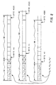
- FIG. 1 a digital communication system which constitutes one preferred embodiment of the present invention will be described.
- This Fig. 1 communication system includes a transmitter circuit 10, four repeater circuits 11, 12, 13 and 14, and a receiver circuit 15. All of these circuits 10-15 are serially coupled to each other through respective bit-serial communication channels 20-24 as shown.
- the transmitter 10 receives a continuous input series of data bits S i on an input terminal 10a; and these bits are received at a bit rate BR i .
- This input series S i can be any sequence of 1's and 0's, and the small portion of the series which is shown in Fig. 1 is merely an example.
- the bit rate BR i can be any substantially constant bit rate; and the rate of 10 9 bits per second which is given in Fig. 1 is just one example.
- This continuous output bit series S o consists of the data bits from the input series S i divided into spaced-apart data blocks, with a fixed number of data bits per block, and a respective output header inserted before each block.
- bit series S o is shown as ...H 0 DB,H 0 DB,... where DB indicates a data block, H 0 indicates an output header, and the dots indicate that the series continues.
- This output bit series S o occurs at a bit rate BR x which is faster than the input bit rate BR i .
- Bit rate BR x is equal to BR i +BR H + ⁇ 1 where BR H is a nominal increase in the bit rate BR i which is made so the headers can be inserted, and ⁇ 1 is a tolerance in that nominal increase.
- bit rate BR H is 10 7 bits per second and ⁇ 1 is 200 bits per second.
- the continuous output bit series S o travels to the repeater 11 where it is received on an input terminal 11a.
- the repeater 11 uses the continuous bit series S o which it is receiving to generate a different continuous series of bits S 1 on an output terminal 11b.
- This new bit series S 1 from the output terminal 11b is shown in Fig. 1 as ...H 1 DB,H 1 DB,.... where each DB represents one of the data blocks that is being received, each H 1 represents a output header from the repeater 11, and the dots indicate that the series continues.
- Each output header H 1 is generated in the repeater 11 by occasionally adding bits to/subtracting bits from a header H 0 which is received on the input terminal 11a. Bits are added if the output series of bits S 1 occurs at a bit rate BR 1 which is slightly faster than the bit rate BR x . Bits are subtracted if the output series of bits S 1 occurs at a bit rate which is slightly slower than the bit rate BR x . Bit rate BR 1 equals the bit rate BR x plus a tolerance of ⁇ 2 bits per second.
- each of the remaining repeaters 12, 13 and 14 operate in the same fashion as the above-described repeater 11.
- the continuous series of bits S 1 travels to the repeater 12 where it is received on an input terminal 12a.
- the repeater 12 uses the series of bits S 1 which it is receiving to transmit a different continuous output series of bits S 2 on an output terminal 12b.
- Bit series S 2 is shown in Fig. 1 as ...H 2 DB,H 2 DB... where each DB represents a data block that is received, each H 2 represents an output header which is generated in the repeater 12 by occasionally adding bits to/subtracting bits from a header H 1 that is received, and the dots indicate that the series continues.
- Bit series S 2 occurs at a bit rate BR 2 which equals the bit rate BR 1 plus a tolerance of ⁇ 3 bits per second.
- each DB is a data block that is received
- each H 3 is an output header which is generated in the repeater 13 by occasionally adding bits to/subtracting bits from the headers H 2 that are received, and the dots indicate that the series continues.
- Bit series S 3 occurs at a bit rate BR 3 which equals bit rate BR 2 plus a tolerance of ⁇ 4 bits per second.
- bit series S 4 is shown in Fig. 1 as...H 4 DB,H 4 DB...where each DB is a data block that is received, and each H 4 is an output header which is generated in the repeater 14 by occasionally adding bits to/subtracting bits from the received headers H 3 .
- Bit series S 4 occurs at a bit rate BR 4 which equals BR 3 plus a tolerance of ⁇ 5 bits per second.
- the continuous series of bits S 4 travels to an input terminal 15a on the receiver 15. Then, the receiver 15 uses the series of bits S 4 that it is receiving to transmit a continuous output series of bits S R on an output terminal 15b which is identical to input series of bits S i to the transmitter 10. To generate the bit series S R , the receiver 15 strips the headers H 4 from the bit series S 4 which it receives; and it sends the remaining data bits to output terminal 15b at a bit rate BR R which is substantially the same as bit rate BR i . Consequently, the two series of bits S R and S i are essentially identical in both their bit values and their speed of occurrence.
- bit series S i to the transmitter input occurs at a bit rate BR i whereas bit series S o from the transmitter output occurs at a faster bit rate BR x which equals BR i +BR H + ⁇ 1 .
- bit rate increase of BR H the headers H o can be inserted before each data block DB in the series S o such that the data bits from the input series S i do not continually accumulate inside of the transmitter 10.
- bit rate BR i 10 9 bits per second and the bit rate BR x is 10 9 +10 7 bits per second
- a total of 10 7 extra bits are sent from the transmitter every second in comparison to the number of bits which the transmitter receives.
- the ratio BR x BR i equal to the total number of bits per header and data block divided by the number of bits per data block
- the bits in the input series S i will not accumulate within the transmitter 10 over time.
- the tolerance terms ⁇ 1 through ⁇ 5 which respectively occur in the bit rates BR x through BR 4 . Due to. these tolerance terms, the respective bit rates of the bit series S o through S 4 do not track each other; but instead, they are independent of each other. For example, the tolerance term ⁇ 2 makes the bit rate BR 1 of the series S 1 independent of the bit rates for the remaining series So, S 2 , S 3 , and S 4 .
- the headers H o through H 4 are generated in the transmitter 10 and repeaters 11-14 with three different lengths; and these different length headers, along with a data block DB which follows each header, is shown in Fig. 2.
- NH indicates a normal length header
- LH indicates a long header
- SH indicates a short header.
- a normal length header NH consists of five bytes which in Fig. 2 are represented by five squares.
- a long header consists of six bytes which in Fig. 2 are represented by six squares; and a short header consists of four bytes which in Fig. 2 are represented by four squares.
- the first three bytes are labeled C 1 , C 2 , and C 3 . These three bytes together constitute a predetermined code which identifies the start of the header.
- the fourth byte contains a number.
- a normal header is identified by the number "1"; a long header is identified by the number "2"; and a short header is identified by the number "0.”
- Following the number "1" in a normal header is one dummy byte which in Fig. 2 is represented by an "X"; and following the number "2" in a long header are two dummy bytes which in Fig. 2 are represented by two "Xs". No dummy bytes follow the "0" in a short header.
- each of the headers H 0 , H 1 , H 2 , H 3 , and H 4 which respectively occur in the bit sequences S 0 through S 4 can be either a normal header, a long header, or a short header.
- the headers H 0 , H 1 , H 2 , H 3 , and H 4 can respectively be normal, normal, short, normal, and normal; whereas at another time instant, the headers H 0 , H 1 , H 2 , H 3 , and H 4 can respectively be normal, long, normal, normal and normal.
- Fig. 3 is in the form of a table which has five rows 31-35 and four columns 36-39.
- Row 31 contains information which relates to the transmitter 10;
- row 32 contains information which relates to the repeater 11;
- row 33 contains information which relates to the repeater 12;
- row 34 contains information which relates to the repeater 13; and
- row 35 contains information which relates the repeater 14.
- Column 36 indicates whether the respective output bit rate from the transmitter 10 and the repeaters 11-14 is fast or slow relative to a nominal bit rate where all of the tolerances ⁇ 1 through ⁇ 5 are zero.
- transmitter 10 is running fast by +200 bits per second
- repeater 11 is running slow by -500 bits per second
- repeater 12 is running slow by -100 bits per second
- repeater 13 is running fast by +250 bits per second
- repeater 14 is running fast by +100 per second.
- Column 38 gives the difference between the number of bits which are received by each repeater and transmitted from the repeater for each second of operation. For the repeater 11, seven hundred more bits are received than are transmitted; for the repeater 12, four hundred more bits are transmitted than are received; for the repeater 13, three hundred fifty more bits are transmitted than are received; and for the repeater 14, one hundred fifty more bits are received than are transmitted.
- the short headers SH are occasionally generated on the output terminal so that more time is available to retransmit the data bits in the data blocks that are being received.
- the long headers are occasionally generated so that more time is available to accumulate the data bits in the data blocks for retransmission.
- column 39 This occasional generation of a long header or a short header is shown in column 39 which lists the ratio of the number of normal headers per short header, and the number of normal headers per long header.
- Each of the entries in column 39 is derived by using five hundred bytes per data block and five bytes per normal header as shown in Fig. 2.
- FIG. 3 shows that when the output bit rate of a repeater is slow, that repeater may occasionally need to generate either a short header or a long header on its output terminal.
- the slow repeater 11 in row 32 occasionally generates a short header; whereas the slow repeater 12 in row 33 occasionally generates a long header.
- the output bit rate of a repeater is fast, that repeater may occasionally need to generate either a long header or a short header; and this is illustrated by the entries in the rows 34 and 35.
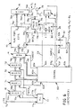
- FIG. 4 a circuit which constitutes one preferred embodiment of the transmitter 10 will be described.
- This Fig. 4 embodiment includes several circuit components 40-55, and each component is described below in TABLE 1.
- ITEM DESCRIPTION 40 Component 40 is a serial-in, parallel-out register which has a serial input 40a; a parallel output 40b, and a clock input 40c.
- Register 40 holds a total of eight bits (one byte). On the rising edge of each clock pulse that is received on the clock input 40c, one bit is loaded into register 40 from input terminal 40a, and the last seven bits which were previously loaded from input 40a are shifted within register 40 by one bit position.
- Component 41 is a register which has a byte-wide input 41a, a byte-wide output 41b, and a clock input 41c. One byte is loaded into register 41 each time the rising edge of a clock pulse occurs on the clock input 41c.
- 42 Component 42 is a dual port, first-in, first-out, memory ("FIFO"). Memory 42 has a byte-wide input port 42a, a write control input 42b, a byte-wide output port 42c, and a read control input 42d. One byte is loaded into the memory 42 each time the rising edge of a pulse is received on input 42b. All bytes which are loaded into the memory 42 travel within the memory to the output port 42c in the same order in which they are loaded.
- a different byte is sent to the output port 42c each time the; rising edge of a pulse occurs on input 42d.
- Memory 42 holds a total of sixteen bytes.
- 43 Component 43 is a digital scrambler circuit which has a byte-wide input 43a and a byte-wide output 43b. Each byte which is received on the input is presented on the output in a scrambled fashion. Due to this scrambling operation, the bits which occur on output 43b are randomized. Consequently the. probability of those bits matching the predetermined code C 1 C 2 C 3 which occurs in the headers of Fig. 2 approaches zero; and, any DC component in the transmitted bit series S o is minimized.
- Component 44 is 2X1 multiplexer which has two byte wide inputs 44a and 44b, one byte wide output 44c, and a control input 44d. A byte is transferred from input 44a to output 44c when a control signal INSERT on input 44d is false; and a byte is transferred from input 44b to output 44c when the control signal INSERT is true.
- 45 Component 45 is a parallel-in, serial-out register which has a parallel input 45a, a serial output 45b, a clock input 45c, and a load control input 45d. One byte is loaded into register 45 each time the rising edge of a clock pulse occurs on input 45c while a LD signal on input 45d is true.
- phase locked oscillator PLO
- Input 46a receives the continuous input series of data bits S i from terminal 10a; and the phase locked oscillator 46 internally has a phase locked loop which locks on to the bit series S i and thereby generates a clock signal CK i on output 46b at nearly the same bit rate as the input bit series S i .
- Component 47 is a divide by eight counter which generates a byte clock BYCK i on its output terminal by dividing the clock signal CK i from the phase locked oscillator by eight.
- 48 Component 48 is a counter which has two inputs 48a and 48b, and one output 48c. Each time a pulse is received on input 48a, the counter 48 counts up by one; and each time a pulse is received on input 48b, the counter 48 counts down by one. Output 48c provides the result of this up and down counting with the signal CNT.
- 49 Component 49 is a crystal oscillator that has one output on which the clock CK o is generated. Since component 49 is a crystal oscillator, the clock signal CK o is very stable and has essentially no jitter.
- Clock signal CK o occurs at the previously described bit rate BR x which equals BR i +BR H + ⁇ 1 .
- the term ⁇ 1 enables the oscillator 49 to have a frequency tolerance which can arise due to a variety of factors such as tolerances in manufacturing, operating temperature, supply voltage, etc.
- the tolerance term ⁇ 1 is no more than plus or minus two parts per million.
- 50 Component 50 is a pulse generator which has one input 50a, and two outputs 50b and 50c. Input 50a receives clock signal CK o and output 50b generates byte clock pulses BYCK o which occur at one-eighth the frequency of the clock signal CK o .
- Each pulse BYCK o lasts for one cycle of clock CK o ; and during the next cycle of clock CK o , a load pulse LD is generated on output 50c.
- 51 Component 51 is counter which has a clock input 51a, a reset input 51b and an output 51c. Each time the rising edge of a clock pulse is received on input 51a while a control signal INSERT on input 51b is true, the counter 51 initializes itself to the number of bytes per data block. That initial count is decremented by one each time the rising edge of a clock signal is received on input 51a while the control signal INSERT is false; and the resulting count occurs on the output 51c.
- 52 Component 52 is a zero detect circuit.
- component 52 When the count from counter 51 is zero, component 52 generates a control signal Z in a true state; whereas when the count from counter 51 is not zero, component 52 generates the signal Z in a false state.
- 53 Component 53 is a sequential control circuit which has three inputs 53a-53c, and two outputs 53d-53e. Input 53a receives the count signals CNT from counter 48; input 53b receives the byte clock BYCK o from pulse generator 50; and input 53c receives the signal Z from the zero detect circuit 52. In response to these three inputs, control circuit 53 generates the headers H o , one byte at a time, as the signal HB on output 53d.
- control circuit 53 generates the control signal INSERT on output 53e which indicates when the header bytes HB are to be inserted.
- Component 54 is a digital AND gate, and component 55 is a digital inverter. When the INSERT control signal is false, component 54 generates a down pulse DN for each cycle of the byte clock BYCK o ; whereas when the INSERT signal is true, component 54 generates no DN pulses.
- the input series of data bits S i sequentially passes from the input terminal 10a through the components 40, 41, 42, 43, 44, and 45 to the output terminal 10b. Passage of the input series of data bits through the registers 40 and 41 and into the FIFO 42 occurs in response to the clock signals CK i and BYCK i ; whereas passage of those data bits from the FIFO 42 through the scrambler 43, the multiplexer 44, and the parallel-in, serial-out register 45 occurs in response to the clock signals CK o and BYCK o .
- control circuit 53 monitors the signal Z from the zero detect circuit 52. When signal Z goes true, the last byte of a data block is being sent from register 45. In response, control circuit 53 generates the INSERT signal in a true state; and that causes the header bytes HB to pass from the control circuit output 53d through multiplexer 44 and into register 45. Control circuit 53 continues to generate the INSERT signal in a true state until the last byte of the header has been inserted into register 45; and then control circuit 53 generates the INSERT signal in a false state.
- control circuit 53 sends a total of five header bytes HB through the multiplexer 44 to the register 45; and this is accomplished by generating the INSERT control signal in a true state for a total of five cycles of the byte clock BYCK o .
- control circuit 53 responds by generating a short header rather than a normal header.
- control circuit 53 responds by generating a long header.
- the control circuit 53 determines whether to generate a normal header, or a long header, or a short header.
- control circuit 53 If the count CNT from counter 48 is within a predetermined range PR, then control circuit 53 generates a normal header. If the count CNT from counter 48 is less than the predetermined range PR, then control circuit 53 generates a' long header. If the count CNT from counter 53 is greater than the predetermined range PR, then control circuit 54 generates a short header. This operation of control circuit 53 is indicated in Fig. 4 by reference numeral 60.
- control circuit 53 To generate a short header, control circuit 53 sends four header bytes HB on its output terminal 53d and it generates the INSERT control signal in a true state during four cycles of the byte clock BYCK o . To generate a long header, control circuit 53 sends six header bytes HB on its output 53d, and it generates the INSERT control signal in a true state for a total of six cycles of the byte clock BYCK o .
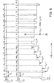
- waveform 61 shows the content of register 41; waveform 62 shows the output of multiplexer 44; and waveform 63 shows the count signal CNT from the counter 48.
- the first byte in register 41 is labeled B i ; the next byte is labeled B i +1; etc.
- a different byte is loaded into register 41 at the start of each byte clock BYCK i ; and thus register 41 holds each byte for a time period T i which is the reciprocal of the byte clock BYCK i .
- the first byte from multiplexer 44 is shown as byte number 499 in a data block of 500 bytes; and the next byte is shown as byte number 500. Then, the next five bytes from the multiplexer 44 are bytes HB 1 -HB 5 which constitute the bytes of a normal header. Then, the next byte from multiplexer 44 is the first byte of a data block; the next byte from the multiplexer 44 is the second byte of the data block; etc.
- a different byte is sent from the multiplexer at the start of each cycle of the byte clock BYCK o ; and thus each byte from the multiplexer lasts for a time period T 0 which is the reciprocal of the byte clock BYCK o .
- the counter 48 is incremented but it is not decremented. This is shown in Fig. 5 wherein the counter 48 is incremented five times from an initial count of C 0 to C 0 +5. Thereafter, when the header bytes are not being sent from the multiplexer 44, the counter 48 is incremented by the byte clock BYCK i , and the counter 48 is decremented by the down pulses DN. Over time, the net effect of this incrementing and decrementing is that the counter 48 counts down because the down pulses DN occur at a faster rate than byte clock BYCK i . This effect can be seen in the portion of the CNT signal which occurs in Fig. 5 after the last header byte H 5 .
- the control circuit 53 By monitoring the count signal CNT from the FIFO counter 48, the control circuit 53 is able to keep that count within the predetermined range PR.
- the predetermined range is shown as C 0 -1 through C 0 +6 as one example. If the count CNT falls below C 0 -1, then control circuit 53 generates a long header for a data block; and that causes the count CNT to increment one more time. Conversely, if the count signal CNT rises above C 0 +6, then control circuit 53 generates a short header for a data block; and that causes the count CNT to increment one less time.
- ITEM DESCRIPTION 70 Component 70 is a serial-in, parallel-out register which has a serial input 70a, a parallel output 70b, and a clock input 70c. Register 70 holds a total of eight bits (one byte).
- each clock pulse that is received on input 70c On the rising edge of each clock pulse that is received on input 70c, one bit is loaded into register 70 from the input terminal 70a, and the last seven bits which were previously loaded from input 70a are shifted within register 70 by one bit position.
- 71 72, & 73 Each of the components 71, 72 and 73 is a one byte register. Each register has a one byte input, a one byte output, and a clock input. One byte is loaded into each register when the rising edge of a clock pulse occurs on the clock input.
- Component 74 is 2X1 multiplexer. Component 74 has two byte-wide inputs 74a and 74b, one byte-wide output 74c, and a control input 74d.
- 75 Component 75 is a dual port, first-in, first-cut, memory (FIFO).
- Memory 75 has a byte-wide input 75a, a write control input 75b, a byte-wide output 75c, and a read control input 75d.
- One byte is loaded into the memory 75 each time the rising edge of a pulse is received on input 75b. All bytes which are loaded into the memory 75 travel within the memory to the output 75c in the same order in which they are loaded.
- a different byte is sent to the output 75c each time the rising edge of a pulse occurs on input 75d.
- Memory 75 holds a total of sixteen bytes.
- 76 Component 76 is a parallel-in, serial-out register which has a parallel input 76a, a serial output 76b, a clock input 76c, and a load control input 76d.
- One byte is loaded into register 76 each time the rising edge of a clock pulse occurs on input 76c while a LD signal on input 76b is true. That byte is shifted within register 76 by one bit position to the output terminal 76d each time the rising edge of a clock pulse occurs on input 76c while the LD signal is false.
- Component 77 is phase locked oscillator (PLO) which has one input 77a, and two outputs 77b and 77c.
- Input 77a receives the continuous input series of data bits S o from terminal 11a; and the phase locked oscillator 77 internally has a phase locked loop which locks on to the bit series S o and thereby generates a clock signal CK i on output 77b at nearly the same bit rate as the input bit series S i .
- Oscillator 77 also searches for the code C 1 C 2 C 3 that occurs in each of the headers; and it generates a byte clock BYCK i on output 77c which is synchronized with that code and occurs once for every eight cycles of the bit clock CK i .
- Component 78 is a crystal oscillator that has one output on which an output clock CK o is generated. Since component 78 is a crystal oscillator, the clock signal CK o is very stable and has essentially no jitter. Clock signal CK o occurs at the previously described bit rate BR 1 which equals BR x + ⁇ 2 .
- the tolerance term ⁇ 2 enables the oscillator 78 to have a frequency tolerance which can arise due to a variety of factors, such as tolerances in manufacturing, operating temperature, supply voltage, etc. Preferably, the tolerance term ⁇ 2 is no more than plus or minus two parts per million.
- Component 79 is a pulse generator which has two inputs 79a and 79b, and two outputs 79c and 79d.
- Input 79a receives clock signal CK o and input 79b receives an enable signal EN.
- EN When the EN signal is false, the outputs 79c and 79d are at a constant "0.”
- output 79c When the EN signal is true, output 79c generates byte clock pulses BYCK o which occur at one-eighth the frequency of the clock signal CK o .
- Each clock pulse BYCK o has lasts for one cycle of clock CK o ; and during the next cycle of clock CK o , a load pulse LD is generated on output 79d.
- Component 80 is a clocked D-type flip-flop. Component 80 has an output Q which sets to a "1" when a rising edge of the clock BYCK o is received, and which resets to a "0" when a down pulse DN is received. 81 Component 81 is an edge triggered one-shot which has an enable input E and a clock input CK. Component 81 generates a down pulse DN if the enable input E is a "1" when the rising edge of a sample pulse SAMPLE occurs on the clock input CK.
- Component 81 together with component 80, generate one DN pulse for each cycle of the output byte clock BYCK o ; and each DN pulse is synchronized to the input byte clock BYCK i .
- Component 82 is a counter which has two inputs 82a and 82b, and one output 82c. Each time the rising edge of a pulse UP is received on the input 82a, the counter 82 counts up by one; and each time the rising edge of a pulse DN is received on the input 82b, the counter 82 counts down by one. Output 82c provides the net result of this up and down counting by the signal CNT.
- Component 83 is a sequential control circuit which has three inputs 83a-83c, and five outputs 83d-83h.
- Input 83a receives the count signals CNT from counter 82;
- input 83b receives the byte clock BYCK i from the phase locked oscillator 77;
- input 83c receives the bytes from register 71.
- control circuit 83 In response to these three inputs, control circuit 83 generates the headers H 1 one byte at a time as signal HB on the output 83d. Also, control circuit 83 generates the INSERT signal on output 83e which controls when the header bytes HB are to be inserted.
- control circuit 83 generates the UP pulses on output 83d which go to the counter 83 and the FIFO 75. In addition, control circuit 83 generates the SAMPLE pulses on output 83g which trigger the one-shot circuit 81. Also, control circuit 83 generates the EN signal which enables the pulse generator 79.
- Each byte in register 71 is examined by the sequential control circuit 83 to determine when a header is being received, since the start of each header is indicated by the predetermined code C 1 C 2 C 3 .
- the sequential control circuit When a header is not being received, the sequential control circuit generates the INSERT signal in a false state so that register 73 is coupled through multiplexer 74 to the FIFO 75.
- control circuit 83 Conversely, when a header is being received, control circuit 83 generates the INSERT signal in a true state so that the new header bytes HB pass through the multiplexer 74 to the FIFO 75.
- FIG. 7 A timing diagram which illustrates the above operation is shown in Fig. 7.
- waveform 90 shows the byte clock BYCK i ;
- waveform 91 shows the content of register 73; and
- waveform 92 shows the INSERT signal.
- three waveforms 93a, 93b, and 93c show three different sequences of the UP signal. Sequence 93a loads a normal header into the FIFO 75; sequence 93b loads a long header into the FIFO 75; and sequence 93c loads a short header into the FIFO 75.
- counter 82 Each time an UP pulse occurs, counter 82 is incremented by one and a single byte is loaded from multiplexer 74 into the FIFO 75.
- the first pulse (left-most pulse) in waveform 93a loads data byte 500 from register 73 into the FIFO 75.
- the second pulse in waveform 93a loads the first header byte HB 1 into the FIFO 75.
- the sixth pulse of waveform 93 loads the fifth header byte HB 5 into the FIFO 75; and the sixth pulse of waveform 93 loads the first data byte of another data block into the FIFO 75.
- Waveform 93b is the same as waveform 93a, except that it contains two pulses during the time that the fifth header byte HB 5 is being sent through the multiplexer 74. Due to those two pulses, the counter 83 is incremented twice; and the fifth header byte is loaded twice into the FIFO 75. This is how a long header is generated within the Fig. 6 repeater.
- Waveform 93c also is the same as waveform 93a, except that during the time that the fifth header byte is passing through the multiplexer 74, no pulses are generated in the UP signal. Consequently, counter 83 is not incremented; and no header byte is loaded into the FIFO 75. This is how, a short header is generated in the Fig. 6 repeater.
- the enable signal EN to the pulse generator 79 When the enable signal EN to the pulse generator 79 is false, the clock pulses BYCK o are forced to a "0"; and consequently, no data bytes are removed from the FIFO 75.
- the control circuit 83 can cause the FIFO 75 to fill half-way with bytes from the multiplexer 74. Thereafter, control circuit 83 generates the EN signal in a true state; and that causes the byte clock BYCK o to be generated.
- the clock signal BYCK o is sent through components 80 and 81.
- Component 80 is a flip-flop which is set to a "1" state each time a rising edge of the clock signal BYCK o occurs; and component 81 generates one down pulse DN if flip-flop 81 is in a "1" state when a rising edge on the signal SAMPLE occurs.
- a pair of waveforms 100 and 101 respectively show the signals UP and SAMPLE.
- This high pulse rate in the SAMPLE signal insures that component 82 will sense each "1" that is set in the flip-flop 81, even if the oscillator 78 is running fast due to its frequency tolerance ⁇ 2 .
- waveforms 102a and 102b two examples of the down pulses DN are shown by waveforms 102a and 102b.
- Waveform 102a occurs when the crystal oscillator 78 has a positive tolerance ⁇ 1 and thus the clock signal BYCK o has a faster than nominal frequency.
- waveform 102b occurs when the crystal oscillator 78 has a negative tolerance ⁇ 1 , and thus the clock signal BYCK o has a slower than nominal frequency.
- the first (left-most) down pulse DN occurs simultaneously with the first (left-most) UP pulse in waveform 101. Due to this simultaneous occurrence of the DN pulse and UP pulse, count C o in the counter 82 remains unchanged. Likewise, the second and third down pulses DN in waveform 102a occurs simultaneously with respective UP pulses in waveform 100.
- the fourth DN pulse in waveform 102a occurs by itself with no corresponding UP pulse in waveform 100. consequently, count C o in the counter 82 is decremented by "1"; and this indicates that the output oscillator 78 is running faster than the nominal frequency. Thereafter, the count in counter 78 switches back and forth between two counts of C 0 and C 0 -1 in response to the UP and down DN pulses as shown. That operation continues for many data blocks in accordance with the normal header per long header ratios that were previously described in conjunction with column 39 of Fig. 3. But eventually, since the crystal oscillator 78 is running fast, another down DN pulse will be generated with no corresponding UP pulse.
- control circuit 83 In response to the count signal CNT from counter 82 and the bytes which are received from register 71, control circuit 83 loads either a normal header, a short header, or a long header into the FIFO 75 as shown in Fig. 9.
- This figure is in the form of a table which has three columns 110, 111, and 112.
- Column 110 shows the type of header which is received by control circuit 83 from register 71; and
- column 111 shows the corresponding count which is received by control circuit 83 from the counter 82.
- control circuit 83 loads the header which is shown in column 112 into the FIFO 75.
- the top-most row in Fig. 9 indicates that when a normal header NH is received from register 1 by control circuit 83 while the count CNT from counter 82 is within a predetermined range PR, the control circuit 83 loads a normal header NH into the FIFO 75.
- the fourth row from the top of the Fig. 9 table shows that when a normal header NH is received from register 1 while the count CNT is greater than the predetermined range, the control circuit 83 loads a short header SH into the FIFO 75.
- the seventh row from the top of the Fig. 9 table indicates that when a normal header NH is received from register 1 while the count from the counter 82 is less than the predetermined range PR, the control circuit 83 loads a long header LH into the FIFO 75.
- Fig. 9 shows that the operation of the control circuit 83 can be summarized as follows.
- a header is received from register 71 while the count CMT is greater than the predetermined range, a corresponding header which is shorter by one byte is generated in the FIFO 75, unless a short header was received.
- a header is received from register 71 while the count from counter 82 is less than the predetermined range, a corresponding header which is longer by one byte is generated in the FIFO 75, unless a long header was received.
- the header which is received from register 71 is duplicated in the FIFO 75.
- This operation by the control circuit 83 is identified in Fig. 9 by reference numerals 115a, 115b, and 115c.
- control circuit 83 checks the count which is received from counter 82 for several consecutive headers. For example, control circuit 83 can check the count which is received from counter 82 for twenty consecutive headers. Then, if the count for a large percentage (e.g. - 75%) of those headers is greater than the predetermined range, the action indicated by reference numeral 115a is taken; and if the count for a large percentage (e.g. 75%) of those headers is less than the predetermined range, the action indicated by reference numeral 115b is taken.
- any transient fluctuations in the count signal CNT from the counter 83 will not cause unnecessary length changes between the headers that are transmitted and received.
- ITEM DESCRIPTION 120 is a serial-in, parallel-out register which as a serial input 120a, a byte-wide parallel output 120b, and a clock input 120c. On the rising edge of each clock pulse that is received on input 120c, one bit is loaded into register 120 from the input terminal 120a, and the last seven bits which were previously loaded from input 120a are shifted within register 120 by one bit position.
- 121 122,& 123 Each of the components 121, 122 and 123 is a one byte register.
- Each register has a byte-wide input, a byte-wide output, and a clock input. One byte is loaded into each register when the rising edge of a clock pulse occurs on the clock input.
- Component 124 is a dual port, first-in, first-out, memory ("FIFO").
- Memory 124 has a byte-wide input port 124a, a write control input 124b, and a byte-wide output port 124c, and a read control input 124d.
- One byte is loaded into memory 124 each time the rising edge of a pulse is received on input 124b. All bytes which are loaded into the memory 124 travel within the memory to the output port 124c in the same order in which they are loaded.
- a different byte is sent to the output port 124c each time the rising edge of a pulse occurs on the input 124d.
- Memory 124 holds a total of thirty-two bytes.
- 125 Component 125 is a descrambler which has a byte-wide input and a byte-wide output. On each byte that is received, component 125 performs a descrambling operation which is the inverse of the scrambling operation that is performed by component 43 in the Fig. 4 transmitter 10; and the result occurs on the output of component 125.
- 126 Component 126 is a parallel-in, serial-out register which has a byte-wide parallel input 126a, a serial output 126b, a clock input 126c, and a load control input 126d.
- One byte is loaded into register 126 each time the rising edge of a clock pulse occurs on input 126c while a LD signal on input 126b is true. That byte is shifted within register 126 by one bit position to the output terminal 126b each time a clock pulse occurs on input 126c while the LD signal is false.
- 127 Component 127 is phase locked oscillator (PLO) which has an input 127a, and two outputs 127b and 127c. Input 127a receives the continuous input series of data bits S 4 ; and the phase locked oscillator 127 internally has a phase locked loop which locks on to that input series of bits S 4 .
- PLO phase locked oscillator
- oscillator 127 By locking on to the S 4 bit series, oscillator 127 is able to generate a clock signal CK i on the output 127b which oscillates at nearly the same bit rate as the bit rate BR 4 of the input bit series S 4 .
- Oscillator 127 also searches for the code C 1 C 2 C 3 that occurs in each of the headers; and it generates a byte clock BYCK i on output 127c which is synchronized with that code and occurs once for every eight cycles of the bit clock CK i .
- 128 Component 128 is a voltage controlled oscillator (VCO) which has one input 128a and one output 128b. Input 128a receives an analog control voltage V c ; and in response.
- VCO voltage controlled oscillator
- oscillator 128 generates a clock CK o on output 128b.
- 129 Component 129 is a pulse generator which has two inputs 129a and 129b, and two outputs 129c and 129d.
- Input 129a receives a clock signal CK o and input 129b receives an enable control signal EN.
- EN enable control signal
- the outputs 129c and 129d are at a constant "0.”
- output 129c When the EN signal is true, output 129c generates down pulses DN which occur at one-eighth the frequency of the clock signal CK o .
- Each pulse DN lasts for one cycle of clock CK o , and during the next cycle of clock CK o , a load pulse LD is generated on output 129d.
- 130 Component 130 is a counter which has two inputs 130a and 130b, and one output 130c. Each time an UP pulse is received on the input 130a, the counter 130 counts up by one; and each time a DOWN pulse is received on the input 130b, the counter 130 counts down by one. Output 130c provides the net result of this up and down counting as the signal CNT. Also, logic circuitry is incorporated into the counter 130 which stops the count CNT from rolling over past a count of zero and past a maximum count.
- Component 131 is a count analyzer which has two inputs 131a, and 131b which respectively receive the count signal CNT from counter 130, and a control signal HDR. In response to these two input signals, component 131 generates speed-up pulses SUP and slow-down pulses SDN on an output 131c, and these pulses respectively cause the analog control voltage V c for the VCO 128 to increase or decrease. When no pulses SUP or SDN are being generated, output 131c is in a high impedance state which approximates an open circuit.
- Component 132 is a low pass filter which has an input which receives the speed-up pulses SUP and slow-down pulses SDN; and which filters those pulses to thereby generate the analog control voltage V c for the VCO 128.
- 133 & 134 Component 133 is a digital inverter, and component 134 is a two input digital AND gate. These two components, together generate the UP pulses for the counter 130 and the FIFO 124.
- inverter 133 inhibits the clock BYCK i from passing through AND gate 134; and consequently, the UP pulses are a constant "0."
- the control signal HDR is false, the clock BYCK i passes through the AND gate 133 to thereby generate the UP pulses.
- 135 Component 135 is a sequential control circuit which has two inputs 135a and 135b, and two outputs 135c and 135d. Input 135a receives each byte which is held in register 121; and input 135b receives the byte clock BYCK i from the phase locked oscillator 127. In response to these two inputs, control circuit 135 generates the HDR signal on output 135c.
- Control signal HDR goes true when the first byte of a header is in register 123, and it goes false when the first byte of a data block is in register 123.
- Control signal HDR is generated within the control circuit 135 by examining the bytes which are received from register 121 to detect the predetermined code C 1 C 2 C 3 which indicates the start of a header, and by examining the next byte which follows that code to determined the length of the header.
- Control circuit 135 also generates the enable signal EN on output 135d. When the EN signal is false, no down pulses DN are generated by the pulse generator 129; and consequently, no bytes are removed from the FIFO 124. Control circuit 135 generates the EN signal in a false state to initially fill the FIFO 124 half way. Thereafter, control circuit 135 always generates the EN control signal in a true state.
- bit series S 4 travels one bit at a time to register 120; and from there the bits are transferred one byte at a time through registers 121, 122, and 123. Each byte that is loaded into register 121 is examined by the sequential control circuit 135 to determine if a header is being received.
- control circuit 135 While register 123 holds the first byte of a header, control circuit 135 generates the HDR signal in a true state on output 135c; and that state is maintained until register 123 holds the first byte of a data block.
- components 133 and 134 prevent the UP pulses from occurring; and consequently, the header bytes in the input series of bits S 4 are not loaded into the FIFO 124.
- each pulse of the byte clock BYCK i passes through AND gate 134 to thereby generate a corresponding UP pulse.
- Each UP pulse loads one data byte from register 123 into the FIFO 124 and increments the count CNT in the counter 130 by one.
- a new data byte is transferred within the FIFO 124 to the output port 124c where it is descrambled by component 125; and in addition, the count CNT from the counter 130 is decremented by one. Then, in response to each load pulse LD from the pulse generator 129, one byte of data is transferred from the descrambler 125 into the parallel-in, serial-out register 125. That byte is then shifted bit by bit to the output terminal 15b.
- the count signals CNT are sent to the count analyzer 131 which checks to see if the count is within a predetermined range. If the maximum count CNT gets so large that it goes outside of the predetermined range, the count analyzer 131 generates speed-up pulses SUP on output 131c such that the analog control voltage V c for the VCO 128 is slightly increased. Conversely, if the minimum count CNT falls below the predetermined range, then the count analyzer 131 generates slow down pulses SDN on output 131c such that the analog control voltage V c for the VCO is slightly decreased.
- Clock signal CK o from the VCO 128 increases in frequency as the analog control voltage V c is increased; and vice-versa.
- By slightly increasing the frequency of the clock signal CK o a few more down pulses DN from by the pulse generator 129 occur; and thus the maximum count from the counter 130 slowly decreases.
- Conversely, by slightly decreasing the frequency of the clock signal CK o a few less down pulses DN from the pulse generator 129 occur; and thus the minimum count from the counter 130 slowly increases.
- waveform 140 shows the content of register 121
- waveform 141 shows the output from the FIFO 124
- waveform 142 shows the count CNT from the counter 130.
- register 121 receives a normal header NH followed by a data block DB i ; then register 121 receives a long header LH followed by a data block DB i-1 ; and then register 121 receives a normal header NH followed by a data block DB i+2 . Due to the operation of the control circuit 135, all of the data blocks but none of the headers are loaded into the FIFO 124. Consequently, in the FIFO output as shown by waveform 141, only the data blocks occur.
- the counter 130 does not receive any UP pulses but it does receive DN pulses. Thus when the headers are being received, the counter 130 counts down; and this occurs in waveform 142 during the time intervals 143a-143d.
- Each time interval 143a, 143c, and 143d corresponds to the receipt of a normal header NH which is five bytes long; and consequently, during those time intervals, the counter 130 is decremented five times.
- time interval 143b corresponds to the receipt of a long header which is six bytes long; and consequently during time interval 143b, the counter 130 is decremented six times.
- the bytes of the data blocks DB are loaded into the FIFO 124 and removed therefrom.
- counter 130 is both incremented and decremented.
- the rate at which data bytes are removed from the FIFO 124 is slower than the rate at which the data bytes are loaded into the FIFO.
- the count CNT in counter 130 gradually increases. This increase, together with the count decrease which occurs during the time intervals 143a-143d give the count waveform 142 a sawtooth shape.
- the count analyzer 131 If the minimum count which is sensed by the count analyzer 131 lies below the predetermined range PR, then the count analyzer 131 generates the slow down pulses SDN such that the frequency of the clock signal CK o from the voltage control oscillator 128 is decreased by just a few cycles per second. Due to this slight decrease in frequency, the minimum count will slowly rise such that after several dozen data blocks DB pass through the FIFO 124, the minimum count will again be back within the predetermined range PR. This slow increase in the minimum count indicated in Fig. 11 by reference numeral 150.
- the count analyzer 131 responds by generating the speed up pulses SUP such that the frequency of the clock signal CK o from the VCO is increased by just a few cycles per second. As a result, the maximum count will slowly decrease; and after several dozen data blocks DB pass through the FIFO, the maximum count will again be within the predetermined range.
- the VCO 128, the pulse generator 129, the counter 130, the count analyzer 131, and the low pass filter 132 together form a closed loop feedback circuit.
- This loop automatically selects the frequency of the clock signal CK o such that the count CNT from the counter 130 stays within the predetermined range PR. Consequently, the output series of bits S R is continuous even though the headers were stripped from the input series of bits S 4 .
- the closed loop feedback circuit 128-132 maintains the count CNT as a sawtooth shaped waveform with a substantially constant average value N A . Consequently, the bit rate of the clock signal CK o is constant and automatically matches the bit rate of the original series of bits S i which occur at the input of the transmitter 10. Thus, the output series of bits S R from the receiver 15 essentially duplicates the input series of bits S i to the transmitter 10.
- the speed-up pulses SUP and slow down pulses SDN only make small changes to the frequency of the clock CK o to thereby minimize jitter.
- the SUP and SDN pulses change the frequency of the clock CK o by increments of less than five-hundred parts per billion, with a total adjustment range of one hundred parts per million.
- the counter 130 incorporates logic circuitry which prevents the count CNT from rolling over. If the count CNT is allowed to roll past zero, the slow down pulses SDN would then switch to speed up pulses SUP; and if the count CNT is allowed to roll past a maximum count, the speed up pulses SUP would then switch to slow down pulses SDN.
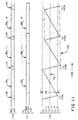
- Fig. 12 One modification is shown in Fig. 12 wherein the continuous input series of data bits S i , which occurs on input terminal 10a of the transmitter 10, consists of 'digital samples of speech. These digital samples of speech are generated by a microphone 150, a sample and hold circuit 151, and an analog-to-digital converter 152 which are serially intercoupled to each other as shown in Fig. 12.
- the continuous input series of data bits S i which occurs on input terminal 10a of the transmitter 10 consists of pixels in successive video frames. These pixels are generated by a camera 160, a sample and hold circuit 161, and an analog-to-digital converter 162 which are serially intercoupled to each other as shown in Fig. 13.
- bit serial communication channels 20-24 which intercouple the transmitter 10, the repeaters 11-14, and the receiver 15 to each other, can be optical channels, wireless channels, or electrical channels.
- the illustrated channel is comprised of a voltage-to-optical converter 170, an optical fibre 171, and an optical-to-voltage converter 172 which are serially intercoupled.
- illustrated channel is comprised of a modulator 180, a transmitting antenna 181, a wireless communication media 182, (such as air or space), a receiving antenna 182, and a demodulator 183, all of which are serially intercoupled.
- the illustrated channel is comprised of a co-axial cable 190.
- the transmitter 10 can be changed such that it receives a continuous stream of data bits which consists of multiple input series of bits that occur simultaneously in a bit-parallel fashion; and the receiver 15 can also be changed such that it duplicates those same bit series in an output stream from the receiver.
- This modification will now be described in conjunction with Figs 17 and 18.
- Fig. 17 shows the input portion of a transmitter which is a modification to the transmitter of Fig. 4.
- the continuous input series of data bits S i is again received on input terminal 10a; and simultaneously, another continuous input series of data bits S i ' is received on another input terminal 10a'.
- Input bit series S i is partitioned into groups of four bits by a four bit wide serial-parallel register 40a'. Simultaneously, the bit series S i ' is partitioned into groups of four bits by a similar register 40b'.
- Fig. 18 shows the output portion of a receiver which is a modification to the Fig. 10 receiver.
- bytes are loaded into the FIFO 124 in the same manner that bytes are loaded into the FIFO 124 of Fig. 10 receiver by components 120, 121, 122, 123, 127, 133, 134 and 135.
- each byte is partitioned into two groups of four bits each.
- One four-bit group is loaded into a four bit wide parallel-in, serial-out register 126a', while the other four-bit group is simultaneously loaded into similar register 126b'.
- That loading of the registers 126a' and 126b' occurs once for each four cycles of the output bit clock CK o which is generated by the VCO 128, since the pulse generator circuit 129' generates the down pulses DN and the load pulses LD once for every four cycles of the bit clock CK o .
- Bit series S R essentially duplicates the input series of bits S i which occurs as an input to the Fig. 17 receiver; and bit series S R ' essentially duplicates the bit series S i ' which occurs as another simultaneous input to the Fig. 17 transmitter.
- each of the headers which are sent from the transmitter 10 and the repeaters 11-14 can be changed to include a field which indicates the number of bytes that occur in the immediately following data block.
- An example of this modification is shown in Fig. 19, wherein the normal header NH includes a four-byte number N 1 N 2 N 3 N 4 which equals the total number of bytes in the immediately following data block DB.
- the number of bytes which are in a data block can vary from one data block to another.
- the transmitter of Fig. 4 generates the number N 1 N 2 N 3 N 4 as part of the header bytes HB which are sent from the sequential control circuit 53 to the multiplexer 44; and that number is also loaded into the DB counter 51. Then, within each repeater of Fig. 6, the number N 1 N 2 N 3 N 4 passes from register 71 through the sequential control circuit 83 to the multiplexer 74; and circuit 83 allows the following data block of N 1 N 2 N 3 N 4 bytes to go into the FIFO 75. Thereafter, within the receiver of Fig.
- the number N 1 N 2 N 3 N 4 is sent from register 121 to the sequential control circuit 135; and in response to that number, the sequential control circuit 135 generates the HDR signal in a false state for a total of N 1 N 2 N 3 N 4 bytes.
- the number of dummy bits which are in a normal header NH and a long header LH can respectively be any number X and 2X; where X preferably is an integer which ranges from 1-64.
- X preferably is an integer which ranges from 1-64.
- Fig. 20 wherein each square represents a group of X bits rather an eight-bit byte.
- the normal header NH contains X dummy bits
- the long header LH contains 2X dummy bits
- the control code C 1 C 2 C 3 is three groups of X bits
- the data block DB is several consecutive groups of X bits each.
- phase locked oscillator 127 generates the BYCK i pulses once for every X cycles of the clock CK i ; and pulse generator 129 generates the LD pulse and DN pulse once for every X cycles of the clock CK o .
- the dual port FIFO which is included in the transmitter 10, the repeaters 11-14, and the receiver 15 can have practically any desired storage capacity.
- a FIFO with a large storage capacity is not needed; and that in turn reduces the corresponding cost of the FIFO.
- the FIFO within the transmitter, the repeaters, and the receiver preferably has a storage capacity of less than 64 bytes.
- the data processing system of Fig. 1 can be modified to include multiple receivers 15, each of which have an input terminal 15a that is coupled to one of the channels 20-24. In such a system, all of those receivers can regenerate the transmitter input series of data bits S i on their output terminal 15b in the same manner as the previously described receiver 15 of Fig. 10.
- the headers which are sent from the transmitter 10 and the repeaters 11-14 can be changed to include a field which indicates that the immediately following data block is to be received by only a particular one of the receivers; and this modification is shown in Fig. 21. There, each of the headers includes a field "R" which identifies one particular receiver that is to receiver the immediately following data block DB.
- the Fig. 10 receiver is changed such that the sequential control circuit 135 examines the field R in each header as it is held in register 121. If that field R matches a particular number which is assigned to the receiver, the control circuit 135 generates the header signal HDR in a false state to pass the immediately following data block DB into the FIFO 124. Otherwise, if a mismatch occurs, the sequential control circuit 135 keeps the header signal HDR in a true state while the immediately following data block DB passes through register 123. To allow for the irregular manner in which data is loaded into the FIFO 124, the storage capacity of that FIFO and the predetermined range PR may have to be increased to more than 64 bytes.
- the headers which are sent from the transmitter 10 and the repeaters 11-14 can be modified to include fields which identifies certain portions of each data block which are to be received by the various receivers.
- An example of this modification is shown in Fig. 22.
- the field S 1 S 1 S 1 specifies the number of the byte in the immediately following data block at which the receiver R 1 starts its receiving operation; and the field E 1 E 1 E 1 specifies the number of the byte in the data block at which the receiver R 1 ends its receiving operation.
- the field S 2 S 2 S 2 specifies the number of the byte in the immediately following data block DB at which the receiver R 2 starts its receiving operation and the field E 2 E 2 E 2 specifies the number of the byte in the data block at which the receiver R 2 ends its receiving operation.
- the Fig. 10 receiver is changed such that the sequential control circuit 135 monitors the header characters as they are held in register 121. If a match is found between the header field R 1 and a number which is assigned to the receiver, then the sequential control circuit 135 generates the header signal HDR in a false state while the characters #S 1 S 1 S 1 through #E 1 E 1 E 1 of the immediately following data block DB are held in register 123. Similarly, if the sequential control circuit 135 finds a match between the, header field R 2 and a number which is assigned to the receiver, then the sequential control circuit 135 generates the header signal HDR in a false state while the characters #S 2 S 2 S 2 through #E 2 E 2 E 2 are held in register 123.
- the storage capacity of that FIFO and the predetermined range PR may have to be increased to more than 64 bytes.
- bit rate BR R will still be substantially constant. This result occurs due to the operation of the closed loop feedback control circuit which is formed by components 128-132 in the Fig. 10 receiver.
- the receiver output bit rate BR R will no longer equal the transmitter input bit rate BR i . Instead, bit rate BR R will equal the one particular constant rate which keeps the count CNT from the counter 130 within the predetermined range PR.
- the digital communication system of Fig. 1 can be modified such that any number of repeaters serially interconnect the transmitter 10 to the receiver 15.
- the Fig. 1 digital communication system can be modified such that the transmitter 10 is connected directly to the receiver 15 with no repeaters there between.
- the independent oscillator 49 within the transmitter 10 and the independent oscillator 78 within the repeaters 11-14 need not be a crystal oscillator.
- those oscillators 49 and 78 can be any oscillator that generates highly stable clock signals independent of the phased-locked oscillators 46 and 77 which also are in the transmitter and the repeaters respectively.
- the oscillators 49 and 78 can be a Cesium atomic clock, or a ceramic resonator.
- the sequential control circuits 53, 83, 135, which are respectively in the Fig. 4 transmitter, the Fig. 6 repeater, and the Fig. 10 receiver can be implemented as a special purpose sequential state machine, or a programmable microprocessor.
Landscapes
- Engineering & Computer Science (AREA)
- Computer Networks & Wireless Communication (AREA)
- Signal Processing (AREA)
- Time-Division Multiplex Systems (AREA)
- Synchronisation In Digital Transmission Systems (AREA)
Claims (61)
- Ein Kommunikationssystem, das der Art ist, die eine Ausgabebitrate sendet, die unabhängig von einer Eingabebitrate ist, um die Summierung von Jitter zu vermeiden, und die Felder veränderlicher Länge verwendet, um die unterschiedlichen Bitraten zu kompensieren, dadurch gekennzeichnet, dass das Kommunikationssystem aus folgendem besteht:wobei der Empfänger weiterhin eine Rückkopplungssteuerschaltung (128-132) mit geschlossener Schleife einschließt, die mit dem Empfängerspeicher (124) gekoppelt ist, die eine Empfänger-Ausgabebitrate auswählt, die im wesentlichen konstant ist und die die gespeicherten Datenbits aus dem Empfängerspeicher (124) als kontinuierlicher Bitstrom (SR und 141) bei der im wesentlichen konstanten Ausgabebitrate in den Ausgabeport (15b) liest, so dass die Anzahl von Bits im Empfängerspeicher ungeachtet der Sender-Eingabebitrate in einem vorbestimmten Bereich bleibt.einem Sender (10), der einen Eingabeport (10a) hat, der nur einen kontinuierlichen Eingabestrom von Datenbits (Si) mit einer Sendereingabe-Bitrate (BRi) empfängt, einen mit dem Eingabeport verbundenen Einzel-Eingabe/Einzel-Ausgabe-Senderspeicher (42) hat, der vorübergehend nur den Eingabestrom von Datenbits (Si) speichert, und eine zwischen dem Senderspeicher (42) und einem Ausgabeanschluss (10b) gekoppelte digitale Senderlogikschaltung (43, 44, 53, 45) hat, die simultan die gespeicherten Datenbits in voneinander beabstandeten bit-seriellen Datenblöcken (DB) mit jeweiligen bit-seriellen Kopfzeilen (NH, LH, SH) sendet, die eine veränderliche Länge haben und den Raum zwischen den Datenblöcken ausfüllen;einem Empfänger (15), der einen Eingabeanschluss (15a) hat, der mit dem Sender gekoppelt ist, der die voneinander beabstandeten Datenblöcke und alle Kopfzeilen, die den Raum dazwischen ausfüllen, empfängt, und der weiterhin eine digitalen Empfängerlogikschaltung (120-123, 135), gefolgt von einem Einzel-Eingabe/Einzel-Ausgabe-Empfänger-Speicher (124), einschließt, die zwischen dem Eingabeanschluss (15a) und einem Ausgabeport (15b) in Reihe gekoppelt sind; worin die digitale Empfängerlogikschaltung Steuersignale (UP, HDR) erzeugt, die in dem Empfängerspeicher nur ausgewählte Bits in den empfangenen Datenblöcken, aber keine Bits aus den Kopfzeilen speichern; und
- Ein System nach Anspruch 1, worin der Sender (10) einen Oszillator (49) einschließt, der Taktsignale erzeugt, die von der Sender-Eingabebitrate unabhängig sind und durch die die Datenblöcke und Kopfzeilen gesendet werden.
- Ein System nach Anspruch 2, worin der Sender (10) mittels eines Repeaters (11) mit dem Empfänger (15) gekoppelt ist, der Datenblöcke und Kopfzeilen bei einer Repeater-Eingabebitrate empfängt und der simultan die Datenblöcke mit gelegentlich modifizierten Kopfzeilen bei einer Repeater-Ausgabebitrate, die anders ist als die Repeater-Eingabebitrate und davon unabhängig ist, weitersendet,.
- Ein System nach Anspruch 3, worin der Repeater die modifizierten Kopfzeilen durch das gelegentliche Addieren/Subtrahieren von Bits zu/von den Kopfzeilen erzeugt, die er empfängt (60).
- Ein System nach Anspruch 4, worin die Kopfzeilen veränderlicher Länge (NH, LH, SH) N oder N+X oder N-X Bits lang sind, worin N und X Ganzzahlen sind.
- Ein System nach Anspruch 1, worin die Rückkopplungssteuerschaltung mit geschlossener Schleife im Empfänger (15) weiterhin eine mit dem Empfängerspeicher (124) verbundene Zählerschaltung (130) einschließt, die einen Zählwert (CNT) erzeugt, die die in den Empfängerspeicher geschriebene Anzahl von Datensbits minus die aus dem Empfängerspeicher gelesenen Anzahl von Datenbits darstellt; und einen Oszillator (128) mit veränderlicher Frequenz einschließt, der von der Zählerschaltung zum Empfängerspeicher gekoppelt ist, der die Empfänger-Ausgabebitrate so auswählt, dass der Zählwert in dem vorbestimmten Bereich bleibt.
- Ein System nach Anspruch 6, worin der Oszillator mit veränderlicher Frequenz. Taktsignale erzeugt, die die gespeicherten Datenbits aus dem Empfängerspeicher mit einer kleineren Frequenz lesen, wenn der Zählwert unter den vorbestimmten Bereich fällt, und mit einer höheren Frequenz lesen, wenn der Zählwert über den vorbestimmten Bereich steigt.
- Ein System nach Anspruch 7, worin der Oszillator mit veränderlicher Frequenz die Frequenz der Taktsignale in Inkrementen von weniger als fünfhundert Teilen pro Billion erhöht und senkt.
- Ein System nach Anspruch 8, worin die Zählerschaltung das Herunterzählen stoppt, wenn sie eine untere Grenze erreicht, und das Heraufzählen stoppt, wenn sie eine obere Grenze erreicht.
- Ein System nach Anspruch 1, worin der Sender-Eingabeport ein Einzel-Eingabeanschluss (10a) ist, auf dem der Eingabestrom von Datenbits auf eine bit-serielle Art und Weise empfangen wird, und worin der Empfänger-Ausgabeport ein Einzel-Ausgabeanschluss (15b) ist, auf dem der Ausgabestrom von Datenbits auf eine bit-serielle Art und Weise erzeugt wird.
- Ein System nach Anspruch 1, worin der Sender-Eingabeport mehrere Eingabeanschlüsse (10a + 10a') hat, auf denen der Eingabestrom von Datenbits auf eine bit-parallele Art und Weise empfangen wird, und worin der Empfänger-Ausgabeport mehrere Ausgabeanschlüsse (15b und 15b') hat, auf denen der Ausgabestrom von Datenbits auf eine bit-parallele Art und Weise erzeugt wird.
- Ein System nach Anspruch 1, worin die Datenbits auf dem Sender-Eingabeport digitale Abtastungen von kontinuierlicher Sprache (150, 151, 152) sind.
- Ein System nach Anspruch 1, worin die Datenbits auf dem Sender-Eingabeport Bildpunkte in sukzessiven Bildrahmen (160, 161, 162) sind.
- Ein System nach Anspruch 1, worin der Sender mittels eines Lichtleiterkanals (171) mit dem Empfänger verbunden ist.
- Ein System nach Anspruch 1, worin der Sender mittels eines koaxialen Kabelkanals (190) mit dem Empfänger verbunden ist.
- Ein System nach Anspruch 1, worin der Sender mittels eines drahtlosen Kanals (182) mit dem Empfänger verbunden ist.
- Ein System nach Anspruch 1, worin der Empfänger den Ausgabestrom von Datenbits aus allen Datenbits in allen der Datenblöcken erzeugt, und worin die Rückkopplungssteuerschaltung mit geschlossener Schleife die Empfänger-Ausgabebitrate dazu zwingt, mit der Sender-Eingabebitrate gleich zu sein.
- Ein System nach Anspruch 1, worin der Empfänger den Ausgabestrom von Datenbits aus allen der Datenbits in auswählten Datenblöcken der Datenblöcke erzeugt.
- Ein System nach Anspruch 1, worin der Empfänger den Ausgabestrom von Datenbits aus den ausgewählten Abschnitten der Datenbits in allen der Datenblöcken erzeugt.
- Ein elektronischer Sender (10), der der Art ist, die eine Ausgabebitrate sendet, die unabhängig von einer Eingabebitrate ist, um die Summierung von Jitter zu vermeiden, und die Felder veränderlicher Länge verwendet, um die unterschiedlichen Bitraten zu kompensieren, dadurch gekennzeichnet, dass sich der Sender zusammensetzt aus:worin die digitale Logikschaltung (43, 44, 53, 45) die Ausgabekopfzeilen mit einer veränderlichen Länge (NH, LH, SH) so einfügt, dass ein Zählwert (CNT) der Anzahl von Datenbits, die an der Sender-Eingabebitrate empfangener werden, während die Kopfzeilen eingefügt werden (RHDR), minus die Differenz zwischen der an der Senderausgabe-Bitrate gesendeten und der an der Sendereingabe-Bitrate empfangenen Anzahl von Datenbits, wenn die Kopfzeilen nicht eingefügt werden ((T-R)NHDR), innerhalb eines vorbestimmten Bereichs (60) bleibteinem Eingabeport (10a), auf dem nur ein kontinuierlicher Eingabestrom von Datenbits (Si) bei einer Sendereingabe-Bitrate (BRi) empfangen wird;einem mit dem Eingabeport verbundenen Einzel-Eingabe/Einzel-Ausgabe-Speicher (42), der vorübergehend nur den Eingabestrom von Datenbits (Si) speichert; undeiner zwischen dem Speicher (42) und einem Ausgabeanschluss (10b) gekoppelte digitale Logikschaltung (43, 44, 53, 45), die eine kontinuierliche Ausgabe-Bitserie (So) am Ausgabeanschluss (10b) erzeugt, und zwar bei einer Senderausgabe-Bitrate (BRx), die schneller ist als die Sendereingabe-Bitrate (BRi) und davon unabhängig ist, worin die Ausgabebitserie (So) aus allen gespeicherten Datenbits (Si) aus dem Speicher (42) in voneinander beabstandeten Datenblöcken (DB) mit einer vor jedem Block eingefügten jeweiligen Ausgabekopfzeile (Ho) besteht; und
- Ein Sender (10) nach Anspruch 20, worin die digitale Logikschaltung einen Oszillator (49) einschließt, der Taktsignale erzeugt, die die Ausgabekopfzeilen und die Datenblöcke in den Ausgabeport senden, und der unabhängig von der Rate schwingt, bei der der Eingabestrom von Datenbits empfangen wird.
- Ein Sender (10) nach Anspruch 21, worin der Oszillator ein Kristall-Oszillator ist.
- Ein Sender (10) nach Anspruch 21, worin die digitale Logikschaltung die Ausgabekopfzeilen mit einer Länge von gerade N Bits (NH) oder N+X (LH) Bits oder N-X (SH) Bits erzeugt, worin N und X Ganzzahlen sind.
- Ein Sender (10) nach Anspruch 23, worin die digitale Logikschaltung folgendes einschließt:eine Zählerschaltung, die ein Zählwertsignal erzeugt, das den Zählwert darstellt; und worindie digitale Logikschaltung die Ausgabekopfzeilen mit folgendem erzeugt:1) N+X Bits, wenn das Zählwertsignal eine untere Grenze erreicht;2) N-X Bits, wenn das Zählwertsignal eine obere Grenze erreicht; und anderenfalls3) mit N Bits.
- Ein Sender (10) nach Anspruch 24, worin die digitale Logikschaltung die Ausgabekopfzeilen mit N Bits mindestens tausend mal häufiger erzeugt als die Ausgabekopfzeilen mit N+X Bits oder N-X Bits.
- Ein Sender (10) nach Anspruch 25, worin X 64 nicht übersteigt.
- Ein Sender (10) nach Anspruch 20, worin der Speicher zu jedem Zeitpunkt nicht mehr als 512 Bits speichert.
- Ein Sender (10) nach Anspruch 20, worin der Eingabeport einen einzigen Anschluss (10a) hat, auf dem der Eingabestrom von Datenbits auf eine bit-serielle Art und Weise empfangen wird.
- Ein Sender (10) nach Anspruch 20, worin der Eingabeport mehrere Anschlüsse (10a, 10a') hat, auf denen der Eingabestrom von Datenbits auf eine bit-parallele Art und Weise empfangen wird.
- Ein Sender (10) nach Anspruch 20, worin jeder der Datenblöcke dieselbe Anzahl von Datenbits hält.
- Ein Sender (10) nach Anspruch 20, worin die Datenblöcke unterschiedliche Anzahlen von Datenbits halten.
- Ein elektronischer Repeater (11), der der Art ist, die bei einer Ausgabebitrate sendet, die von einer Eingabebitrate unabhängig ist, um die Summierung von Jitter zu vermeiden, und der Felder veränderlicher Länge verwendet, um die unterschiedlichen Bitraten zu kompensieren, dadurch gekennzeichnet, dass sich der Repeater zusammensetzt aus:einem Eingabeanschluss (11a), auf dem eine kontinuierliche Eingabereihe von Bits (So) bei einer Repeater-Eingabebitrate (BRx) empfangen wird, die eine verschachtelte Sequenz von Eingabekopfzeilen (Ho) und Datenblöcken (DB) bildet;einem Ausgabeanschluss (11b), auf dem eine kontinuierliche Ausgabereihe von Bits (S1) bei einer Repeater-Ausgabebitrate (BR1) gesendet wird, die ungleich der Repeater-Eingabebitrate und davon unabhängig ist und die eine verschachtelte Sequenz von Ausgabekopfzeilen (H1) und der Datenblöcke (DB) bildet; undeiner digitalen Logikschaltung (70-74 und 83), gefolgt von einem Einzel-Eingabe/Einzel-Ausgabe-Speicher (75), die zwischen dem Eingabeanschluss (11a) und dem Ausgabeanschluss (11b) in Reihe gekoppelt werden, worin die digitale Logikschaltung die Datenblöcke durchläuft und die Ausgabekopfzeilen ohne Bedingung erzeugt, indem exklusiv Bits zu den Eingabekopfzeilen addiert oder exklusiv Bits davon subtrahiert werden, so dass ein Zählwert (CNT) von irgendwelchen addierten Bits minus irgendwelcher subtrahierten Bits (BA-BS) plus die Anzahl von empfangenen Bits (BR) minus die Anzahl von gesendeten Bits (BT) innerhalb eines vorbestimmten Bereichs bleibt, und worin der Speicher (75) vorübergehend nur die durchgelassenen Datenblöcke und Ausgabekopfzeilen aus der digitalen Logikschaltung ohne Modifikation an dem Ausgabeanschluss (75c, 11b) für das Senden speichert.
- Ein Repeater (11) nach Anspruch 32, worin die digitale Logikschaltung einen Oszillator (78) einschließt, der Taktsignale erzeugt, die die Ausgabekopfzeilen und die Datenblöcke in den Ausgabeanschluss senden, und der unabhängig von der Rate schwingt, bei der die Eingabereihe von Bits empfangen wird.
- Ein Repeater (11) nach Anspruch 33, worin der Oszillator ein Kristall-Oszillator ist.
- Ein Repeater (11) nach Anspruch 33, worin die Eingabekopfzeilen aus N Bits (NH) oder N+X Bits (LH) oder N-X Bits (SH) bestehen, worin N und X Ganzzahlen sind; und worin die digitale Logikschaltung die Ausgabekopfzeilen so erzeugt, dass sie ebenfalls aus N Bits (NH) oder N+X Bits (LH) oder N-X Bits (SH) bestehen.
- Ein Repeater (11) nach Anspruch 35, worin die digitale Logikschaltung folgendes einschließt:eine Zählerschaltung (82), die ein Zählwertsignal (CNT) erzeugt, das den Zählwert darstellt; und worindie digitale Logikschaltung die Ausgabekopfzeilen erzeugt, indem:1) X Bits zu einer Eingabekopfzeile addiert werden, wenn die Eingabekopfzeile empfangen wird, während das Zählwertsignal unter einem vorbestimmten Bereich liegt, außer wenn die Eingabekopfzeile N+X Bits enthält (115b);2) X Bits von der Eingabekopfzeile subtrahiert werden, wenn die Eingabekopfzeile empfangen wird, während das Zählwertsignal über dem vorbestimmten Bereich liegt, außer wenn die Eingabekopfzeile N-X Bits enthält (115a), und anderenfalls3) die Eingabekopfzeile kopiert wird (115c).
- Ein Repeater (11) nach Anspruch 36, worin X 64 nicht übersteigt.
- Ein Repeater (11) nach Anspruch 32, worin der Speicher zu jedem Zeitpunkt nicht mehr als 512 Bits speichert.
- Ein Repeater (11) nach Anspruch 32, worin die digitale Logikschaltung Bits mit einer Frequenz von weniger als einmal pro Tausend Eingabekopfzeilen zu der Eingabekopfzeile addiert oder Bits davon subtrahiert.
- Ein Repeater (11) nach Anspruch 32, worin jeder der Datenblöcke dieselbe Anzahl von Datenbits hält.
- Ein Repeater (11) nach Anspruch 32, worin die Datenblöcke verschiedene Anzahlen von Datenbits halten.
- Ein Verfahren zum Betreiben eines elektronischen Repeaters der Art, die eine Ausgabebitrate sendet, die unabhängig von einer Eingabebitrate ist, um die Summierung von Jitter zu vermeiden, und die Felder veränderlicher Länge verwendet, um die unterschiedlichen Bitraten zu kompensieren; dadurch gekennzeichnet, dass das Verfahren, einschließlich folgender Schritte, folgendes umfasst:das Empfangen an einem Eingabeanschluss (11a), bei einer Repeater-Eingabebitrate, einer kontinuierlichen Reihe von Bits, die eine verschachtelte Sequenz von Eingabekopfzeilen und Datenblöcken bildet;das Senden an einem Ausgabeanschluss (11b), bei einer Repeater-Ausgabebitrate, die ungleich der Repeater-Eingabebitrate und unabhängig davon ist, einer kontinuierlichen Reihe von Bits, die eine verschachtelte Sequenz von Ausgabekopfzeilen und Datenblöcken bildet;das Erzeugen der Ausgabekopfzeilen ohne Bedingung in einer digitalen Logikschaltung (70-74 und 83), die mit dem Eingabeanschluss (11a) gekoppelt, indem exklusiv Bits zu den Eingabekopfzeilen addiert oder exklusiv davon subtrahiert werden, so dass ein Zählwert (CNT) irgendwelcher addierten Bits minus irgendwelcher subtrahierten Bits (BA-BS) plus die Anzahl von empfangenen Bits (BR) minus die Anzahl von gesendeten Bits (BT) innerhalb eines vorbestimmten Bereichs bleibt; unddas vorübergehende Speichern von nur den Ausgabekopfzeilen und Datenblöcken in einem Einzel-Eingabe/Einzel-Ausgabe-Speicher (75), der zwischen der Steuerschaltung und dem Ausgabeanschluss (11b) in Reihe gekoppelt ist, damit ohne Modifikation auf dem Ausgabeanschluss gesendet wird.
- Ein Verfahren nach Anspruch 42, worin die Repeater-Ausgabebitrate von einem Oszillator eingestellt wird, der unabhängig von der Repeater-Eingabebitrate schwingt.
- Ein Verfahren nach Anspruch 42, das weiterhin den Schritt zum Beschränken der Eingabekopfzeilen und Datenblöcke einschließt, um aus N Bits oder N+X Bits oder N-X Bits zu bestehen, worin N und X Ganzzahlen sind.
- Ein Verfahren nach Anspruch 42, das weiterhin folgende Schritte einschließt:das Erzeugen einer Ausgabekopfzeile, indem X Bits zu einer Eingabekopfzeile addiert werden, wenn die Eingabekopfzeile empfangen wird, während der Zählwert unter einem vorbestimmten Bereich liegt, außer wenn die Eingabekopfzeile N+X Bits enthält;das Erzeugen der Ausgabekopfzeile, indem X Bits von der Eingabekopfzeile subtrahiert werden, wenn die Eingabekopfzeile empfangen wird, während der Zählwert über dem vorbestimmten Bereich liegt, außer wenn die Eingabekopfzeile N-X Bits enthält; und anderenfallsdas Weiterleiten der Eingabekopfzeile an den Ausgabeanschluss.
- Ein elektronischer Empfänger (15), der der Art ist, die Ausgabebits bei einer Ausgabebitrate erzeugt, die unabhängig von einer Eingabebitrate ist, um die Summierung von Jitter zu vermeiden, und die Felder veränderlicher Länge verwendet, um die unterschiedlichen Bitraten zu kompensieren; dadurch gekennzeichnet, dass sich der Empfänger aus folgendem zusammensetzt:worin die digitale Logikschaltung Steuersignale (HDR, UP) erzeugt, die bewirken, dass der Speicher (124) nur ausgewählte Bits aus den Datenblöcken (DB), aber keine Bits aus den Kopfzeilen (H4) speichert; undeinem Eingabeanschluss (15a), der eine kontinuierliche Reihe von Bits (S4) bei einer Empfänger-Eingabebitrate (BR4) empfängt, die aus Datenbits in voneinander beabstandeten Datenblöcken (DB) mit jeweiligen Kopfzeilen (H4) besteht, die eine veränderliche Länge (NH, LH, SH) haben und die den Raum zwischen den Datenblöcken füllen;einer digitalen Logikschaltung (120-133 und 135), gefolgt von einem Einzel-Eingabe/Einzel-Ausgabe-Speicher (124), die zwischen dem Eingabeanschluss (15a) und einem Ausgabeport (15b) in Reihe geschaltet sind;
einer Rückkopplungssteuerschaltung (128-132) mit geschlossener Schliefe, die an dem Speicher (124) gekoppelt ist, die eine Empfänger-Ausgabebitrate (BRR) auswählt, die im wesentlichen konstant ist und die gespeicherten Bits aus dem Speicher (124) in den Ausgabeport (156) als ein kontinuierlicher Bitstrom (SR) bei der im wesentlichen konstanten Ausgabebitrate liest, und zwar so, dass die Anzahl von Bits im Speicher (124) ungeachtet der Eingabebitrate innerhalb eines vorbestimmten Bereichs (142) bleibt. - Ein Empfänger (15) nach Anspruch 46, worin die Rückkopplungssteuerschaltung mit geschlossener Schleife weiterhin eine an den Speicher (124) gekoppelte Zählerschaltung (130) einschließt, die ein Zählwertsignal (CNT) erzeugt, das die Anzahl der im Speicher gespeicherten Datenbits darstellt; und einen von der Zählerschaltung zum Speicher gekoppelten Oszillator (128) einschließt, der auf das Zählwertsignal reagiert, indem er die im wesentlichen konstante Ausgabebitrate auf eine Art und Weise auswählt, die den Zählwert in einem vorbestimmten Bereich beibehält.
- Ein Empfänger (15) nach Anspruch 47, worin der Oszillator (128) Taktsignale erzeugt, die die gespeicherten Abschnitte der ausgewählten Bits aus dem Speicher lesen; und worin der Oszillator die Taktsignale mit einer Abnahme in der Frequenz erzeugt, wenn der Zählwert unter den vorbestimmten Bereich fällt, und mit einer Zunahme in der Frequenz erzeugt, wenn der Zählwert über den vorbestimmten Bereich steigt.
- Ein Empfänger (15) nach Anspruch 48, worin der Oszillator die Frequenz der Taktsignale in Inkrementen von weniger als fünfhundert Teilen pro Billion erhöht und senkt.
- Ein Empfänger (15) nach Anspruch 49, worin die Zählerschaltung das Herunterzählen stoppt, wenn sie eine untere Grenze erreicht, und das Heraufzählen stoppt, wenn sie eine obere Grenze erreicht.
- Ein Empfänger (15) nach Anspruch 46, worin der Speicher zu irgendeinem Zeitpunkt nicht mehr als 512 der ausgewählten Bits aus den Datenblöcken speichert.
- Ein Empfänger (15) nach Anspruch 46, worin die Datenbits, die in Blöcken empfangen und als kontinuierlicher Strom an den Ausgabeport gesendet werden, digitale Abtastungen von kontinuierlicher Sprache (150, 151, 152) sind.
- Ein Empfänger (15) nach Anspruch 46, worin die Datenbits, die in Blöcken empfangen und als kontinuierlicher Strom an den Ausgabeport gesendet werden, Bildpunkte in sukzessiven Bildrahmen (160, 161, 162) sind.
- Ein Empfänger (15) nach Anspruch 46, worin die Kopfzeilen veränderlicher Länge N oder N+X oder N-X Bits haben, worin N und X Ganzzahlen (NH, LH, SH) sind.
- Ein Empfänger (15) nach Anspruch 46, worin jeder
der Datenblöcke dieselbe Anzahl von Datenbits hält. - Ein Empfänger (15) nach Anspruch 46, worin die Datenblöcke unterschiedliche Anzahlen von Datenbits halten.
- Ein Empfänger (15) nach Anspruch 46, worin der Ausgabeport ein einziger Anschluss (15b) ist, auf dem der Ausgabestrom von Datenbits auf eine bit-serielle Art und Weise gesendet wird.
- Ein Empfänger (15) nach Anspruch 46, worin das Ausgabeport mehrere Anschlüsse hat, auf denen der Ausgabestrom von Datenbits auf eine bit-parallele Art und Weise gesendet wird (15b und 15b').
- Ein Empfänger (15) nach Anspruch 46, worin der Ausgabestrom von Datenbits in allen der Datenblöcke aus allen der Datenbits besteht.
- Ein Empfänger (15) nach Anspruch 46, worin der Ausgabestrom von Datenbits in ausgewählten Datenblöcken der Datenblöcke aus allen der Datenbits besteht.
- Ein Empfänger (15) nach Anspruch 46, worin der Ausgabestrom von Datenbits in allen der Datenblöcke aus ausgewählten Datenbits besteht.
Applications Claiming Priority (9)
| Application Number | Priority Date | Filing Date | Title |
|---|---|---|---|
| US08/656,540 US5680416A (en) | 1996-05-31 | 1996-05-31 | Digital communication system which eliminates cumulative jitter |
| US656538 | 1996-05-31 | ||
| US656540 | 1996-05-31 | ||
| US656541 | 1996-05-31 | ||
| US08/656,536 US5680415A (en) | 1996-05-31 | 1996-05-31 | Repeater for a digital communication system which eliminates cumulative jitter |
| US08/656,541 US5694432A (en) | 1996-05-31 | 1996-05-31 | Transmitter for a digital communication system which eliminates cumulative jitter |
| US656536 | 1996-05-31 | ||
| US08/656,538 US5689531A (en) | 1996-05-31 | 1996-05-31 | Receiver for a digital communication system which eliminates cumulative jitter |
| PCT/US1997/009114 WO1997045974A1 (en) | 1996-05-31 | 1997-05-30 | Digital communication system which eliminates cumulative jitter |
Publications (2)
| Publication Number | Publication Date |
|---|---|
| EP0903022A1 EP0903022A1 (de) | 1999-03-24 |
| EP0903022B1 true EP0903022B1 (de) | 2003-10-29 |
Family
ID=27505292
Family Applications (1)
| Application Number | Title | Priority Date | Filing Date |
|---|---|---|---|
| EP97926788A Expired - Lifetime EP0903022B1 (de) | 1996-05-31 | 1997-05-30 | Summierung von zittern verhinderndes digitales nachrichtenübertragungssystem |
Country Status (4)
| Country | Link |
|---|---|
| EP (1) | EP0903022B1 (de) |
| JP (1) | JP2002502560A (de) |
| DE (1) | DE69725845D1 (de) |
| WO (1) | WO1997045974A1 (de) |
Family Cites Families (7)
| Publication number | Priority date | Publication date | Assignee | Title |
|---|---|---|---|---|
| US4270203A (en) * | 1978-11-13 | 1981-05-26 | Arthur A. Collins, Inc. | Timing adjustment circuit for digital switching |
| US4284843A (en) * | 1979-05-10 | 1981-08-18 | General Electric Company | Repeating station for use in digital data communications link |
| DE3101536A1 (de) * | 1981-01-14 | 1982-09-02 | Heinrich-Hertz-Institut für Nachrichtentechnik Berlin GmbH, 1000 Berlin | Verfahren zur uebermittlung von zeitmultiplexsignalen in einem digitalen nachrichtennetz |
| US4495617A (en) * | 1982-09-09 | 1985-01-22 | A.B. Dick Company | Signal generation and synchronizing circuit for a decentralized ring network |
| DE3525567A1 (de) * | 1985-07-15 | 1987-05-07 | Krone Ag | Bewegtbildkodierer mit selbstkennzeichnung der stopfzeichen |
| JPH01502711A (ja) * | 1987-03-17 | 1989-09-14 | カントニ・アントニオ | デジタル通信リンクにおけるジッタ制御 |
| DE4027968A1 (de) * | 1990-09-04 | 1992-03-05 | Philips Patentverwaltung | Schaltungsanordnung zur bitratenanpassung zweier digitaler signale |
-
1997
- 1997-05-30 EP EP97926788A patent/EP0903022B1/de not_active Expired - Lifetime
- 1997-05-30 WO PCT/US1997/009114 patent/WO1997045974A1/en not_active Ceased
- 1997-05-30 DE DE69725845T patent/DE69725845D1/de not_active Expired - Lifetime
- 1997-05-30 JP JP54292097A patent/JP2002502560A/ja not_active Ceased
Also Published As
| Publication number | Publication date |
|---|---|
| JP2002502560A (ja) | 2002-01-22 |
| WO1997045974A1 (en) | 1997-12-04 |
| EP0903022A1 (de) | 1999-03-24 |
| DE69725845D1 (de) | 2003-12-04 |
Similar Documents
| Publication | Publication Date | Title |
|---|---|---|
| US5241543A (en) | Independent clocking local area network and nodes used for the same | |
| US6639919B2 (en) | Bit-level control for dynamic bandwidth allocation | |
| CA2088156C (en) | Method and means for transferring a data payload from a first sonet signal to a sonet signal of different frequency | |
| EP0088432B1 (de) | Multiplexereinrichtung mit nBmB-Kodierer | |
| US5465254A (en) | Ring-type communication network | |
| EP0268792A2 (de) | Datenübertragungssystem mit Mehrfachausnützung | |
| EP0978961A1 (de) | System und Verfahren zur Phasenrückgewinnung in einem synchronen Kommunikationssystem | |
| CN112187391B (zh) | 一种环路带宽动态调整的过采样时钟数据恢复方法及系统 | |
| EP0342861B1 (de) | Glättungsanordnung für unabhängig getaktete Netzwerke | |
| US5357514A (en) | Distributed bit-by-bit destuffing circuit for byte-stuffed multiframe data | |
| EP0342844B1 (de) | Glättungsanordnung für unabhängig getaktete Netzwerke | |
| JPH08204666A (ja) | 制御回路付き伝送システム及び比較器付き制御回路 | |
| KR100247409B1 (ko) | 비동기성 전송 모드인 디지탈 원거리통신망 단말 장비의 동기화 장치 | |
| EP0545392B1 (de) | Synchrone Schaltung | |
| JPH0738545A (ja) | 平滑出力クロック信号抽出方法 | |
| US5694432A (en) | Transmitter for a digital communication system which eliminates cumulative jitter | |
| US5680415A (en) | Repeater for a digital communication system which eliminates cumulative jitter | |
| US5680416A (en) | Digital communication system which eliminates cumulative jitter | |
| US5689531A (en) | Receiver for a digital communication system which eliminates cumulative jitter | |
| EP0903022B1 (de) | Summierung von zittern verhinderndes digitales nachrichtenübertragungssystem | |
| US5970107A (en) | Synchronous residual time stamp service clock regenerator phase locked loop phase comparator and loop filter | |
| US5680422A (en) | Method and apparatus for reducing waiting time jitter in pulse stuffing synchronized digital communications | |
| WO1996002095A1 (en) | Two stage clock dejitter circuit for regenerating an e4 telecommunications signal from the data component of an sts-3c signal | |
| US6122337A (en) | Modular circuitry architecture for residual time stamp service clock regenerator phase locked loop | |
| EP0308450B1 (de) | Jitterregelung in digitalen übertragungsstrecken |
Legal Events
| Date | Code | Title | Description |
|---|---|---|---|
| PUAI | Public reference made under article 153(3) epc to a published international application that has entered the european phase |
Free format text: ORIGINAL CODE: 0009012 |
|
| 17P | Request for examination filed |
Effective date: 19981218 |
|
| AK | Designated contracting states |
Kind code of ref document: A1 Designated state(s): DE GB |
|
| GRAH | Despatch of communication of intention to grant a patent |
Free format text: ORIGINAL CODE: EPIDOS IGRA |
|
| GRAH | Despatch of communication of intention to grant a patent |
Free format text: ORIGINAL CODE: EPIDOS IGRA |
|
| GRAA | (expected) grant |
Free format text: ORIGINAL CODE: 0009210 |
|
| AK | Designated contracting states |
Kind code of ref document: B1 Designated state(s): DE GB |
|
| REG | Reference to a national code |
Ref country code: GB Ref legal event code: FG4D |
|
| REF | Corresponds to: |
Ref document number: 69725845 Country of ref document: DE Date of ref document: 20031204 Kind code of ref document: P |
|
| PG25 | Lapsed in a contracting state [announced via postgrant information from national office to epo] |
Ref country code: DE Free format text: LAPSE BECAUSE OF FAILURE TO SUBMIT A TRANSLATION OF THE DESCRIPTION OR TO PAY THE FEE WITHIN THE PRESCRIBED TIME-LIMIT Effective date: 20040130 |
|
| PLBE | No opposition filed within time limit |
Free format text: ORIGINAL CODE: 0009261 |
|
| STAA | Information on the status of an ep patent application or granted ep patent |
Free format text: STATUS: NO OPPOSITION FILED WITHIN TIME LIMIT |
|
| 26N | No opposition filed |
Effective date: 20040730 |
|
| PGFP | Annual fee paid to national office [announced via postgrant information from national office to epo] |
Ref country code: GB Payment date: 20120525 Year of fee payment: 16 |
|
| GBPC | Gb: european patent ceased through non-payment of renewal fee |
Effective date: 20130530 |
|
| PG25 | Lapsed in a contracting state [announced via postgrant information from national office to epo] |
Ref country code: GB Free format text: LAPSE BECAUSE OF NON-PAYMENT OF DUE FEES Effective date: 20130530 |