BACKGROUND OF THE INVENTION:
This invention relates to digital communication
systems; and more particularly, it relates to digital
communication systems which operate at bit rates which
are so high that even small amounts of cumulative jitter
will cause reception errors.
One typical prior art digital communication
system to which the present invention relates includes a
transmitter, multiple repeaters, and a receiver; all of
which are serially coupled to each other by communication
channels. In this system, a continuous series of data
bits is passed from the transmitter through each of the
repeaters to the receiver. To perform this operation in
the prior art, the transmitter, the repeaters, and the
receiver each includes a respective phase-locked
oscillator which locks onto the incoming series of bits,
and thereby generates clock signals that determine the
time instants at which the incoming bits are regenerated
on an output terminal.
However, a problem with such a prior art
digital communication system is that the timing for the
serial data streams within the system deviates in an
uncontrolled fashion from the ideal. These uncontrolled
deviations from the ideal timing are herein referred to
as "jitter". This jitter can arise from a number of
factors, such as: variations in power supply voltages,
variations in circuit operating temperatures, noise in
'the communication channels, the inability of the phase-locked
oscillator to perfectly track and perfectly lock
onto an input series of bits; etc.
Further, in the above prior art system, the
jitter problem becomes worse as the number of repeaters
between the transmitter and the receiver increases
because any jitter that is within the bandwidth of a
phase-locked oscillator accumulates from one repeater to
the next repeater. Thus, if the input series of bits to
the first repeater has a slight amount of jitter due to
any source of jitter in the transmitter, then the output
series of bits will have a larger amount of jitter; the
output series of bits from the second repeater will have
an even larger amount of jitter; etc. This cumulative
jitter presents a serious problem for the receiver
because as it increases, the error rate which occurs in
the data that is received by the receiver also increases.
Also, as the bit rate for the series of bits
which passes through the communication system increases,
the error rate that is caused by any fixed amount of
jitter also increases. This increase in error rate
occurs because as the bit rate gets faster, the time
period of each bit gets shorter; and consequently, the
amount of time by which clock signals from a phase-locked
oscillator can vary and still be in proper
synchronization with the incoming bits gets smaller. For
example, in a high speed optical digital communication
system which has a bit rate of 109 bits per second, the
time per bit is only one billionth of a second; and thus,
the amount of high frequency jitter which can be
tolerated before errors will occur is just a fraction of
one-billionth of a second.
Jitter is often expressed in terms of having a
particular amplitude at a particular frequency, where the
amplitude is given as a multiple of one bit period at a
certain nominal bit rate and the frequency is an
oscillation frequency about that bit rate. For example,
jitter in a 100 mega-bit-per-second system can be
expressed as having an amplitude of 1.5 UIpp at 6.5 KHz,
where 1.5 UIpp is (1.5)x(10 nanoseconds) and 6.5 KHz is an
oscillation frequency about 100 mega-bits-per-second.
This same amount of jitter in a 1000 mega-bit-per-second
system is 15 UIpp at 6.5 KHz. In the 100 Mbps system, the
jitter of 1.5 UIpp may be acceptable; whereas, in the 1000
Mbps system, the jitter of 15 UIpp may be totally
unacceptable even though its absolute amplitude is
unchanged.
In the prior art, the problem of cumulative
jitter in a digital communication system is addressed in
the International Patent Application W088/07300 by
Cantoni, et al. (Herein after Cantoni), and in U.S.
Patent 4,270,203 by Collins, et al. (Hereinafter
Collins). Cantoni and Collins both disclose a
communication system of a type where each repeater in the
system transmits at an output bit rate which is
independent of the input bit rate to avoid accumulation
of jitter, and each repeater uses variable length fields
to compensate for the different bit rates.
However, in both Cantoni and Collins, the
structure of the circuits which are disclosed to avoid
the cumulative jitter have several drawbacks. These
circuits are shown in Fig. 3 of Cantoni and Fig. 5 of
Collins.
For example, in the Fig. 3 circuit of Cantoni,
a memory 18 is. required which must have two separate
inputs and two separate outputs that operate in parallel.
One output carries a data signal DX and the other output
carries a frame maker FMX as shown in Fig. 3. This
requirement of two parallel inputs and outputs on the
memory 18 occurs because without the frame marker output
FMX occurring in parallel with the data output DX, a
stuffing control block 28 which changes the stuffing
control field SC simply will not- work. See Figs. 3 and 6
which both show that the signals DX and FMX are sent in
parallel from the memory 18 through a pipeline 24 to the
stuffing control block 28. By comparison, in present
independent claims, the circuits that are recited include
a memory through which two signals cannot be sent in
parallel because each memory is a single-input single-output
memory.
As another example, in the Fig. 3 circuit of
Cantoni all changes to the stuffing control field SC and
the stuffing field SF which are received from the input
terminal are generated by logic circuits which follow the
memory 18. These logic circuits include the stuffing
control block 28 the read pointer 20 which responds to
control signals F0 and F1 from the stuffing control block
28. By comparison, with the present independent claims,
all changes to the input header are made by a digital
logic circuit which precedes the memory, and that changed
input header is stored in the memory for. transmission
without modification as the output header.
Similarly in Collins, an elastic store memory
18 in Fig. 5 stores variable length fields from an input
terminal, and these fields are modified by a digital
logic circuit which follows the memory. Thus, this
structure also is the opposite of what is recited in the
present independent claims.
Accordingly, the primary object of the present
invention is to provide a novel digital communication
system in which the above problem is overcome.
BRIEF SUMMARY OF THE INVENTION:
In accordance with the present invention, a
digital communication system is disclosed which includes
a novel transmitter, multiple novel repeaters, and a
novel receiver; all of which are serially intercoupled to
each other.
One embodiment of the novel transmitter
includes an input terminal on which a continuous input
series of data bits is received at a constant transmitter
input bit rate; and an output terminal on which a
continuous output series of bits are transmitted at a
transmitter output bit rate that is faster than the
transmitter input bit rate. Within this output series of
bits, the input series of data bits is partitioned into
spaced apart blocks and a respective output header is
inserted before each block. To insert the output
headers, a digital logic circuit is included in the
transmitter between the input terminal and the output
terminal. This logic circuit generates the output
headers with a variable length such that a count of the
number of data bits received at the transmitter input bit
rate while the headers are being inserted, minus the
difference between the number of data bits transmitted at
the transmitter output bit rate and received at the
transmitter input bit rate when the headers are not being
inserted, stays within a predetermined range.
Due to the variable length headers which are
generated within the transmitter, the transmitter output
bit rate can be set by clock signals from a crystal
oscillator which is included within the transmitter; and
this crystal oscillator can oscillate independently of
the transmitter input bit rate at which the data bits are
received. Consequently, the transmitter output bit rate
does not need to track the transmitter input bit rate,
and thus no cumulative jitter occurs in the output series
of bits from the output terminal.
One embodiment of each novel repeater is
comprised of an input terminal on which a continuous
input series of bits is received at a repeater input bit
rate; and an output terminal on which a continuous output
series of bits is transmitted at a repeater output bit
rate not equal to the repeater input bit rate. Both the
input bit series and the output bit series consist of an
interleaved sequence of headers and data blocks; but the
headers in the output bit series occasionally differ from
the headers that are received. To generate the output
headers, a digital logic circuit is included in the
repeater between the input terminal and the output
terminal which occasionally adds bits to/subtracts bits
from the input headers such that a count of the number of
bits added minus the number of bits subtracted plus the
number of bits received minus the number of bits
transmitted stays within a predetermined range.
Due to this forming of the output header by
occasionally adding bits to/subtracting bits from the
input headers, the repeater output bit rate can be set by
clock signals from a crystal oscillator within the
repeater which oscillates independently of the rate at
which the input series of bits is received.
Consequently, the repeater output bit rate does not need
to track the repeater input bit rate; and thus no
cumulative jitter occurs in the output series of bits
from the output terminal of each repeater.
One embodiment of the novel receiver is
comprised of an input circuit which receives a continuous
input series of bits at a receiver input bit rate which
consists of spaced apart data blocks, each of which is
preceded by a respective input header. Also, the
receiver includes an output circuit, coupled to the input
circuit, which sends the bits from the data blocks but
not from the headers to an output terminal at a receiver
output bit rate which is slower than the receiver input
bit rate.
Further, this output circuit includes a closed
loop feedback control circuit which selects the receiver
output bit rate such that it is substantially constant
and - a) the bits from the data blocks occur on the
output terminal in a continuous series, and b) a count of
the number of data bits sent to the output terminal when
the data blocks are not being received by the input
circuit, minus the difference between the number of data
bits received by the input circuit and sent to the output
terminal when the data blocks are being received, stays
within a predetermined range. By this means, the closed
loop feedback control circuit forces the receiver output
bit rate to be substantially equal to the transmitter
input bit rate.
BRIEF DESCRIPTION OF THE DRAWINGS:
Various preferred embodiments of the present
invention are described herein in the Detailed
Description in conjunction with the accompanying Figs. 1-22,
wherein:
DETAILED DESCRIPTION:
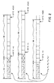
Referring now to Fig. 1, a digital
communication system which constitutes one preferred
embodiment of the present invention will be described.
This Fig. 1 communication system includes a transmitter
circuit 10, four repeater circuits 11, 12, 13 and 14,
and a receiver circuit 15. All of these circuits 10-15
are serially coupled to each other through respective
bit-serial communication channels 20-24 as shown.
In operation, the transmitter 10 receives a
continuous input series of data bits Si on an input
terminal 10a; and these bits are received at a bit rate
BRi. This input series Si can be any sequence of 1's and
0's, and the small portion of the series which is shown
in Fig. 1 is merely an example. Likewise, the bit rate
BRi can be any substantially constant bit rate; and the
rate of 109 bits per second which is given in Fig. 1 is
just one example.
While the continuous input series of data bits
Si is being received, the transmitter 10 generates a
different continuous output series of bits So on an output
terminal 10b. This continuous output bit series So
consists of the data bits from the input series Si divided
into spaced-apart data blocks, with a fixed number of
data bits per block, and a respective output header
inserted before each block.
In Fig. 1, the output bit series So is shown
as ...H0DB,H0DB,... where DB indicates a data block, H0
indicates an output header, and the dots indicate that
the series continues. This output bit series So occurs at
a bit rate BRx which is faster than the input bit rate
BRi. Bit rate BRx is equal to BRi+BRH+Δ1 where BRH is a
nominal increase in the bit rate BRi which is made so the
headers can be inserted, and Δ1 is a tolerance in that
nominal increase. As a numerical example, bit rate BRH is
107 bits per second and Δ1 is 200 bits per second.
From output terminal 10b of the transmitter 10,
the continuous output bit series So travels to the
repeater 11 where it is received on an input terminal
11a. There, the repeater 11 uses the continuous bit
series So which it is receiving to generate a different
continuous series of bits S1 on an output terminal 11b.
This new bit series S1 from the output terminal 11b is
shown in Fig. 1 as ...H1DB,H1DB,.... where each DB
represents one of the data blocks that is being received,
each H1 represents a output header from the repeater 11,
and the dots indicate that the series continues.
Each output header H1 is generated in the
repeater 11 by occasionally adding bits to/subtracting
bits from a header H0 which is received on the input
terminal 11a. Bits are added if the output series of bits
S1 occurs at a bit rate BR1 which is slightly faster than
the bit rate BRx. Bits are subtracted if the output
series of bits S1 occurs at a bit rate which is slightly
slower than the bit rate BRx. Bit rate BR1 equals the bit
rate BRx plus a tolerance of Δ2 bits per second.
Each of the remaining repeaters 12, 13 and 14
operate in the same fashion as the above-described
repeater 11. Thus, from output terminal 11b of the
repeater 11, the continuous series of bits S1 travels to
the repeater 12 where it is received on an input terminal
12a. There, the repeater 12 uses the series of bits S1
which it is receiving to transmit a different continuous
output series of bits S2 on an output terminal 12b. Bit
series S2 is shown in Fig. 1 as ...H2DB,H2 DB... where
each DB represents a data block that is received, each H2
represents an output header which is generated in the
repeater 12 by occasionally adding bits to/subtracting
bits from a header H1 that is received, and the dots
indicate that the series continues. Bit series S2 occurs
at a bit rate BR2 which equals the bit rate BR1 plus a
tolerance of Δ3 bits per second.
Similarly, from output terminal 12b of the
repeater 12, the continuous series of bits S2 travels to
the repeater 13 where it is received on an input terminal
13a. Repeater 13 then uses the series of bits S2 which it
is receiving to transmit a different continuous output
series of bits S3 on an output terminal 13b. This series
S3 equals ...H3DB, H3DB...where each DB is a data block that
is received, each H3 is an output header which is
generated in the repeater 13 by occasionally adding bits
to/subtracting bits from the headers H2 that are received,
and the dots indicate that the series continues. Bit
series S3 occurs at a bit rate BR3 which equals bit rate
BR2 plus a tolerance of Δ4 bits per second.
Likewise, the continuous series of bits S3
travels from the repeater 13 to the repeater 14 where it
is received on an input terminal 14a. Repeater 14 then
uses the series of bits S3 to transmit a different
continuous output series of bits S4 on an output
terminal 14b. Bit series S4 is shown in Fig. 1
as...H4DB,H4DB...where each DB is a data block that is
received, and each H4 is an output header which is
generated in the repeater 14 by occasionally adding bits
to/subtracting bits from the received headers H3. Bit
series S4 occurs at a bit rate BR4 which equals BR3 plus a
tolerance of Δ5 bits per second.
From the repeater 14, the continuous series of
bits S4 travels to an input terminal 15a on the receiver
15. Then, the receiver 15 uses the series of bits S4 that
it is receiving to transmit a continuous output series of
bits SR on an output terminal 15b which is identical to
input series of bits Si to the transmitter 10. To
generate the bit series SR, the receiver 15 strips the
headers H4 from the bit series S4 which it receives; and
it sends the remaining data bits to output terminal 15b
at a bit rate BRR which is substantially the same as bit
rate BRi. Consequently, the two series of bits SR and Si
are essentially identical in both their bit values and
their speed of occurrence.
Now, consider in further detail the two series
of bits Si and So which respectively are received by and
transmitted from the transmitter 10. Bit series Si to the
transmitter input occurs at a bit rate BRi whereas bit
series So from the transmitter output occurs at a faster
bit rate BRx which equals BRi+BRH+Δ1. Due to the bit rate
increase of BRH, the headers Ho can be inserted before
each data block DB in the series So such that the data
bits from the input series Si do not continually
accumulate inside of the transmitter 10.
For example, when the bit rate BRi is 109 bits
per second and the bit rate BRx is 109+107 bits per second,
a total of 107 extra bits are sent from the transmitter
every second in comparison to the number of bits which
the transmitter receives. By keeping the ratio BRxBRi
equal to the total number of bits per header and data
block divided by the number of bits per data block, the
bits in the input series Si will not accumulate within the
transmitter 10 over time. For the case where BRx=109+107
and BRi=109, the above ratio is satisfied by an output
series So which has one hundred bytes in the data block
for each byte in the header.
Next, consider in further detail the tolerance
terms Δ1 through Δ5 which respectively occur in the bit
rates BRx through BR4. Due to. these tolerance terms, the
respective bit rates of the bit series So through S4 do
not track each other; but instead, they are independent
of each other. For example, the tolerance term Δ2 makes
the bit rate BR1 of the series S1 independent of the bit
rates for the remaining series So, S2, S3, and S4.
This independence of the respective bit rates
BRx through BR4 is important because it enables those bit
rates to be set by respective crystal oscillators within
the transmitter 10 and each of the repeaters 11-14. Each
such oscillator generates clock signals that send the
output headers and data blocks to a respective output
terminal 10b-14b independently of the bit rate at which
bits are received on the corresponding input terminals
10a-14a. By generating these clock signals with the
crystal oscillator, as opposed to a phase locked
oscillator which attempts to track the frequency of the
input series of bits that is received, jitter caused by
phase locking is completely eliminated in the series of
bits that are sent from the output terminals 10b-14b.
In order to accommodate the bit rate tolerances
Δ1 through Δ5, the headers Ho through H4 are generated in
the transmitter 10 and repeaters 11-14 with three
different lengths; and these different length headers,
along with a data block DB which follows each header, is
shown in Fig. 2. There, NH indicates a normal length
header; LH indicates a long header; and SH indicates a
short header. A normal length header NH consists of five
bytes which in Fig. 2 are represented by five squares. A
long header consists of six bytes which in Fig. 2 are
represented by six squares; and a short header consists
of four bytes which in Fig. 2 are represented by four
squares.
Within the normal header NH and the long header
LH and the short header SH, the first three bytes are
labeled C1, C2, and C3. These three bytes together
constitute a predetermined code which identifies the
start of the header. Also in the normal header NH and
the long header LH and the short header SH, the fourth
byte contains a number. A normal header is identified by
the number "1"; a long header is identified by the number
"2"; and a short header is identified by the number "0."
Following the number "1" in a normal header is one dummy
byte which in Fig. 2 is represented by an "X"; and
following the number "2" in a long header are two dummy
bytes which in Fig. 2 are represented by two "Xs". No
dummy bytes follow the "0" in a short header.
At any one time instant, each of the headers H0,
H1, H2, H3, and H4 which respectively occur in the bit
sequences S0 through S4 can be either a normal header, a
long header, or a short header. For example, at one time
instant, the headers H0, H1, H2, H3, and H4 can respectively
be normal, normal, short, normal, and normal; whereas at
another time instant, the headers H0, H1, H2, H3, and H4 can
respectively be normal, long, normal, normal and normal.
This point will now be further explained by a specific
example which is shown in Fig. 3.
Fig. 3 is in the form of a table which has five
rows 31-35 and four columns 36-39. Row 31 contains
information which relates to the transmitter 10; row 32
contains information which relates to the repeater 11;
row 33 contains information which relates to the repeater
12; row 34 contains information which relates to the
repeater 13; and row 35 contains information which
relates the repeater 14.
Column 36 indicates whether the respective
output bit rate from the transmitter 10 and the repeaters
11-14 is fast or slow relative to a nominal bit rate
where all of the tolerances Δ1 through Δ5 are zero. One
specific numerical example of these fast or slow bit
rates is given in column 37. In this example,
transmitter 10 is running fast by +200 bits per second;
repeater 11 is running slow by -500 bits per second;
repeater 12 is running slow by -100 bits per second;
repeater 13 is running fast by +250 bits per second; and
repeater 14 is running fast by +100 per second.
Column 38 gives the difference between the
number of bits which are received by each repeater and
transmitted from the repeater for each second of
operation. For the repeater 11, seven hundred more bits
are received than are transmitted; for the repeater 12,
four hundred more bits are transmitted than are received;
for the repeater 13, three hundred fifty more bits are
transmitted than are received; and for the repeater 14,
one hundred fifty more bits are received than are
transmitted.
In those cases where more bits are received
than are transmitted, the short headers SH are
occasionally generated on the output terminal so that
more time is available to retransmit the data bits in the
data blocks that are being received. Conversely, in
those cases where more bits are being transmitted on the
output terminal than are being received, the long headers
are occasionally generated so that more time is available
to accumulate the data bits in the data blocks for
retransmission.
This occasional generation of a long header or
a short header is shown in column 39 which lists the
ratio of the number of normal headers per short header,
and the number of normal headers per long header. Each
of the entries in column 39 is derived by using five
hundred bytes per data block and five bytes per normal
header as shown in Fig. 2.
Inspection of Fig. 3 shows that when the output
bit rate of a repeater is slow, that repeater may
occasionally need to generate either a short header or a
long header on its output terminal. For example, the
slow repeater 11 in row 32 occasionally generates a short
header; whereas the slow repeater 12 in row 33
occasionally generates a long header. Likewise, when the
output bit rate of a repeater is fast, that repeater may
occasionally need to generate either a long header or a
short header; and this is illustrated by the entries in
the rows 34 and 35.
Turning now to Fig. 4, a circuit which
constitutes one preferred embodiment of the
transmitter
10 will be described. This Fig. 4 embodiment includes
several circuit components 40-55, and each component is
described below in TABLE 1.
| (Transmitter Components) |
| ITEM | DESCRIPTION | |
| 40 | Component 40 is a serial-in, parallel-out register which has a serial input 40a; a parallel output 40b, and a clock input 40c. Register 40 holds a total of eight bits (one byte). On the rising edge of each clock pulse that is received on the clock input 40c, one bit is loaded into register 40 from input terminal 40a, and the last seven bits which were previously loaded from input 40a are shifted within register 40 by one bit position. |
| 41 | Component 41 is a register which has a byte-wide input 41a, a byte-wide output 41b, and a clock input 41c. One byte is loaded into register 41 each time the rising edge of a clock pulse occurs on the clock input 41c. |
| 42 | Component 42 is a dual port, first-in, first-out, memory ("FIFO"). Memory 42 has a byte-wide input port 42a, a write control input 42b, a byte-wide output port 42c, and a read control input 42d. One byte is loaded into the memory 42 each time the rising edge of a pulse is received on input 42b. All bytes which are loaded into the memory 42 travel within the memory to the output port 42c in the same order in which they are loaded. A different byte is sent to the output port 42c each time the; rising edge of a pulse occurs on input 42d. Memory 42 holds a total of sixteen bytes. |
| 43 | Component 43 is a digital scrambler circuit which has a byte-wide input 43a and a byte-wide output 43b. Each byte which is received on the input is presented on the output in a scrambled fashion. Due to this scrambling operation, the bits which occur on output 43b are randomized. Consequently the. probability of those bits matching the predetermined code C1 C2 C3 which occurs in the headers of Fig. 2 approaches zero; and, any DC component in the transmitted bit series So is minimized. |
| 44 | Component 44 is 2X1 multiplexer which has two byte wide inputs 44a and 44b, one byte wide output 44c, and a control input 44d. A byte is transferred from input 44a to output 44c when a control signal INSERT on input 44d is false; and a byte is transferred from input 44b to output 44c when the control signal INSERT is true. |
| 45 | Component 45 is a parallel-in, serial-out register which has a parallel input 45a, a serial output 45b, a clock input 45c, and a load control input 45d. One byte is loaded into register 45 each time the rising edge of a clock pulse occurs on input 45c while a LD signal on input 45d is true. That byte is shifted within register 45 by one bit position to output terminal 45b each time the rising edge of a clock pulse occurs on input 45c while the LD signal is false. |
| 46 | Component 46 is phase locked oscillator (PLO) which has one input 46a and one output 46b. Input 46a receives the continuous input series of data bits Si from terminal 10a; and the phase locked oscillator 46 internally has a phase locked loop which locks on to the bit series Si and thereby generates a clock signal CKi on output 46b at nearly the same bit rate as the input bit series Si. |
| 47 | Component 47 is a divide by eight counter which generates a byte clock BYCKi on its output terminal by dividing the clock signal CKi from the phase locked oscillator by eight. |
| 48 | Component 48 is a counter which has two inputs 48a and 48b, and one output 48c. Each time a pulse is received on input 48a, the counter 48 counts up by one; and each time a pulse is received on input 48b, the counter 48 counts down by one. Output 48c provides the result of this up and down counting with the signal CNT. |
| 49 | Component 49 is a crystal oscillator that has one output on which the clock CKo is generated. Since component 49 is a crystal oscillator, the clock signal CKo is very stable and has essentially no jitter. Clock signal CKo occurs at the previously described bit rate BRx which equals BRi+BRH+Δ1. Here, the term Δ1 enables the oscillator 49 to have a frequency tolerance which can arise due to a variety of factors such as tolerances in manufacturing, operating temperature, supply voltage, etc. Preferably the tolerance term Δ1 is no more than plus or minus two parts per million. |
| 50 | Component 50 is a pulse generator which has one input 50a, and two outputs 50b and 50c. Input 50a receives clock signal CKo and output 50b generates byte clock pulses BYCKo which occur at one-eighth the frequency of the clock signal CKo. Each pulse BYCKo lasts for one cycle of clock CKo; and during the next cycle of clock CKo, a load pulse LD is generated on output 50c. |
| 51 | Component 51 is counter which has a clock input 51a, a reset input 51b and an output 51c. Each time the rising edge of a clock pulse is received on input 51a while a control signal INSERT on input 51b is true, the counter 51 initializes itself to the number of bytes per data block. That initial count is decremented by one each time the rising edge of a clock signal is received on input 51a while the control signal INSERT is false; and the resulting count occurs on the output 51c. |
| 52 | Component 52 is a zero detect circuit. When the count from counter 51 is zero, component 52 generates a control signal Z in a true state; whereas when the count from counter 51 is not zero, component 52 generates the signal Z in a false state. |
| 53 | Component 53 is a sequential control circuit which has three inputs 53a-53c, and two outputs 53d-53e. Input 53a receives the count signals CNT from counter 48; input 53b receives the byte clock BYCKo from pulse generator 50; and input 53c receives the signal Z from the zero detect circuit 52. In response to these three inputs, control circuit 53 generates the headers Ho, one byte at a time, as the signal HB on output 53d. Also, control circuit 53 generates the control signal INSERT on output 53e which indicates when the header bytes HB are to be inserted. |
| 54 and 55 | Component 54 is a digital AND gate, and component 55 is a digital inverter. When the INSERT control signal is false, component 54 generates a down pulse DN for each cycle of the byte clock BYCKo; whereas when the INSERT signal is true, component 54 generates no DN pulses. |
All of the components 40-55 within the
transmitter 10 are intercoupled to each other as shown in
Fig. 4; and how those components interact will now be
described in conjunction with Figs. 4 and 5. Within the
transmitter 10, the input series of data bits Si
sequentially passes from the input terminal 10a through
the components 40, 41, 42, 43, 44, and 45 to the output
terminal 10b. Passage of the input series of data bits
through the registers 40 and 41 and into the FIFO 42
occurs in response to the clock signals CKi and BYCKi;
whereas passage of those data bits from the FIFO 42
through the scrambler 43, the multiplexer 44, and the
parallel-in, serial-out register 45 occurs in response to
the clock signals CKo and BYCKo.
Inspection of the input portion of the FIFO 42
in Fig. 4 shows that clock input 42b receives an
uninterrupted clock signal BYCKi ; and consequently, one
byte of data is loaded into the FIFO 42 for each cycle of
the clock BYCKi. By comparison, inspection of the output
portion of the FIFO 42 shows that clock input 42d
receives a byte clock BYCKo which is inhibited when the
control signal INSERT is true. Consequently, when the
INSERT signal is true, the amount of data which is stored
within the FIFO 42 builds up.
To generate the INSERT control signal, the
control circuit 53 monitors the signal Z from the zero
detect circuit 52. When signal Z goes true, the last
byte of a data block is being sent from register 45. In
response, control circuit 53 generates the INSERT signal
in a true state; and that causes the header bytes HB to
pass from the control circuit output 53d through
multiplexer 44 and into register 45. Control circuit 53
continues to generate the INSERT signal in a true state
until the last byte of the header has been inserted into
register 45; and then control circuit 53 generates the
INSERT signal in a false state.
Normally, control circuit 53 sends a total of
five header bytes HB through the multiplexer 44 to the
register 45; and this is accomplished by generating the
INSERT control signal in a true state for a total of five
cycles of the byte clock BYCKo. However, if too much data
has accumulated in the FIFO 42 from the input terminal
10a, then control circuit 53 responds by generating a
short header rather than a normal header. Conversely, if
not enough of data is being stored in the FIFO 42, then
control circuit 53 responds by generating a long header.
Each time a byte is loaded into the FIFO 42,
the counter 48 counts up by one; and each time a byte is
removed from the FIFO 42, the counter 48 is decremented
by one. By monitoring the count signal CNT from the FIFO
counter 48, the control circuit 53 determines whether to
generate a normal header, or a long header, or a short
header.
If the count CNT from counter 48 is within a
predetermined range PR, then control circuit 53 generates
a normal header. If the count CNT from counter 48 is
less than the predetermined range PR, then control
circuit 53 generates a' long header. If the count CNT
from counter 53 is greater than the predetermined range
PR, then control circuit 54 generates a short header.
This operation of control circuit 53 is indicated in
Fig. 4 by reference numeral 60.
To generate a short header, control circuit 53
sends four header bytes HB on its output terminal 53d and
it generates the INSERT control signal in a true state
during four cycles of the byte clock BYCKo. To generate a
long header, control circuit 53 sends six header bytes HB
on its output 53d, and it generates the INSERT control
signal in a true state for a total of six cycles of the
byte clock BYCKo.
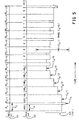
How some of the above-described signals vary as
a function of time within the transmitter 10 can be seen
in Fig. 5. There, waveform 61 shows the content of
register 41; waveform 62 shows the output of multiplexer
44; and waveform 63 shows the count signal CNT from the
counter 48. In Fig. 5, the first byte in register 41 is
labeled Bi; the next byte is labeled Bi+1; etc. A
different byte is loaded into register 41 at the start of
each byte clock BYCKi; and thus register 41 holds each
byte for a time period Ti which is the reciprocal of the
byte clock BYCKi.
Also in Fig. 5, the first byte from multiplexer
44 is shown as byte number 499 in a data block of 500
bytes; and the next byte is shown as byte number 500.
Then, the next five bytes from the multiplexer 44 are
bytes HB1-HB5 which constitute the bytes of a normal
header. Then, the next byte from multiplexer 44 is the
first byte of a data block; the next byte from the
multiplexer 44 is the second byte of the data block; etc.
A different byte is sent from the multiplexer at the
start of each cycle of the byte clock BYCKo; and thus each
byte from the multiplexer lasts for a time period T0 which
is the reciprocal of the byte clock BYCKo.
During the time period that the header bytes
HB1-HB5 are being sent from multiplexer 44, the counter 48
is incremented but it is not decremented. This is shown
in Fig. 5 wherein the counter 48 is incremented five
times from an initial count of C0 to C0+5. Thereafter,
when the header bytes are not being sent from the
multiplexer 44, the counter 48 is incremented by the byte
clock BYCKi, and the counter 48 is decremented by the down
pulses DN. Over time, the net effect of this
incrementing and decrementing is that the counter 48
counts down because the down pulses DN occur at a faster
rate than byte clock BYCKi. This effect can be seen in
the portion of the CNT signal which occurs in Fig. 5
after the last header byte H5.
By monitoring the count signal CNT from the
FIFO counter 48, the control circuit 53 is able to keep
that count within the predetermined range PR. In Fig. 5,
the predetermined range is shown as C0-1 through C0+6 as
one example. If the count CNT falls below C0-1, then
control circuit 53 generates a long header for a data
block; and that causes the count CNT to increment one
more time. Conversely, if the count signal CNT rises
above C0+6, then control circuit 53 generates a short
header for a data block; and that causes the count CNT to
increment one less time.
Next, with reference to Fig. 6, a circuit which
constitutes one preferred embodiment of each repeater
11-14 will be described. For simplicity in Fig. 6, only
the bit series S
0 and S
1 which occur in the
repeater 11
are shown. This Fig. 6 embodiment includes several
circuit components, and each component is described below
in TABLE 2.
| (Repeater Components) |
| ITEM | DESCRIPTION | |
| 70 | Component 70 is a serial-in, parallel-out register which has a serial input 70a, a parallel output 70b, and a clock input 70c. Register 70 holds a total of eight bits (one byte). On the rising edge of each clock pulse that is received on input 70c, one bit is loaded into register 70 from the input terminal 70a, and the last seven bits which were previously loaded from input 70a are shifted within register 70 by one bit position. |
| 71 72, & 73 | Each of the components 71, 72 and 73 is a one byte register. Each register has a one byte input, a one byte output, and a clock input. One byte is loaded into each register when the rising edge of a clock pulse occurs on the clock input. |
| 74 | Component 74 is 2X1 multiplexer. Component 74 has two byte-wide inputs 74a and 74b, one byte-wide output 74c, and a control input 74d. Data is transferred from the input 74a to the output 74c when a control signal INSERT on input 74d is false; and data is transferred from the input 74b to the output 44c when the control signal INSERT is true. |
| 75 | Component 75 is a dual port, first-in, first-cut, memory (FIFO). Memory 75 has a byte-wide input 75a, a write control input 75b, a byte-wide output 75c, and a read control input 75d. One byte is loaded into the memory 75 each time the rising edge of a pulse is received on input 75b. All bytes which are loaded into the memory 75 travel within the memory to the output 75c in the same order in which they are loaded. A different byte is sent to the output 75c each time the rising edge of a pulse occurs on input 75d. Memory 75 holds a total of sixteen bytes. |
| 76 | Component 76 is a parallel-in, serial-out register which has a parallel input 76a, a serial output 76b, a clock input 76c, and a load control input 76d. One byte is loaded into register 76 each time the rising edge of a clock pulse occurs on input 76c while a LD signal on input 76b is true. That byte is shifted within register 76 by one bit position to the output terminal 76d each time the rising edge of a clock pulse occurs on input 76c while the LD signal is false. |
| 77 | Component 77 is phase locked oscillator (PLO) which has one input 77a, and two outputs 77b and 77c. Input 77a receives the continuous input series of data bits So from terminal 11a; and the phase locked oscillator 77 internally has a phase locked loop which locks on to the bit series So and thereby generates a clock signal CKi on output 77b at nearly the same bit rate as the input bit series Si. Oscillator 77 also searches for the code C1 C2 C3 that occurs in each of the headers; and it generates a byte clock BYCKi on output 77c which is synchronized with that code and occurs once for every eight cycles of the bit clock CKi. |
| 78 | Component 78 is a crystal oscillator that has one output on which an output clock CKo is generated. Since component 78 is a crystal oscillator, the clock signal CKo is very stable and has essentially no jitter. Clock signal CKo occurs at the previously described bit rate BR1 which equals BRx+Δ2. Here, the tolerance term Δ2 enables the oscillator 78 to have a frequency tolerance which can arise due to a variety of factors, such as tolerances in manufacturing, operating temperature, supply voltage, etc. Preferably, the tolerance term Δ2 is no more than plus or minus two parts per million. |
| 79 | Component 79 is a pulse generator which has two inputs 79a and 79b, and two outputs 79c and 79d. Input 79a receives clock signal CKo and input 79b receives an enable signal EN. When the EN signal is false, the outputs 79c and 79d are at a constant "0." When the EN signal is true, output 79c generates byte clock pulses BYCKo which occur at one-eighth the frequency of the clock signal CKo. Each clock pulse BYCKo has lasts for one cycle of clock CKo; and during the next cycle of clock CKo, a load pulse LD is generated on output 79d. |
| 80 | Component 80 is a clocked D-type flip-flop. Component 80 has an output Q which sets to a "1" when a rising edge of the clock BYCKo is received, and which resets to a "0" when a down pulse DN is received. |
| 81 | Component 81 is an edge triggered one-shot which has an enable input E and a clock input CK. Component 81 generates a down pulse DN if the enable input E is a "1" when the rising edge of a sample pulse SAMPLE occurs on the clock input CK. Component 81, together with component 80, generate one DN pulse for each cycle of the output byte clock BYCKo; and each DN pulse is synchronized to the input byte clock BYCKi. |
| 82 | Component 82 is a counter which has two inputs 82a and 82b, and one output 82c. Each time the rising edge of a pulse UP is received on the input 82a, the counter 82 counts up by one; and each time the rising edge of a pulse DN is received on the input 82b, the counter 82 counts down by one. Output 82c provides the net result of this up and down counting by the signal CNT. |
| 83 | Component 83 is a sequential control circuit which has three inputs 83a-83c, and five outputs 83d-83h. Input 83a receives the count signals CNT from counter 82; input 83b receives the byte clock BYCKi from the phase locked oscillator 77; and input 83c receives the bytes from register 71. In response to these three inputs, control circuit 83 generates the headers H1 one byte at a time as signal HB on the output 83d. Also, control circuit 83 generates the INSERT signal on output 83e which controls when the header bytes HB are to be inserted. Further, control circuit 83 generates the UP pulses on output 83d which go to the counter 83 and the FIFO 75. In addition, control circuit 83 generates the SAMPLE pulses on output 83g which trigger the one-shot circuit 81. Also, control circuit 83 generates the EN signal which enables the pulse generator 79. |
All of the components 70-83 within the repeater
11 are intercoupled to each other as shown in Fig. 6; and
how those components interact with each other will now be
described. From input terminal 11a, the bit series So
travels to the serial-in parallel-out register 70; and
from there, the bits are transferred one byte at a time
through the registers, 71, 72 and 73. This transfer
occurs in synchronization with the byte clock BYCKi which
is generated by the phase locked loop 77.
Each byte in register 71 is examined by the
sequential control circuit 83 to determine when a header
is being received, since the start of each header is
indicated by the predetermined code C1C2C3. When a header
is not being received, the sequential control circuit
generates the INSERT signal in a false state so that
register 73 is coupled through multiplexer 74 to the FIFO
75. Conversely, when a header is being received, control
circuit 83 generates the INSERT signal in a true state so
that the new header bytes HB pass through the multiplexer
74 to the FIFO 75.
A timing diagram which illustrates the above
operation is shown in Fig. 7. There, waveform 90 shows
the byte clock BYCKi; waveform 91 shows the content of
register 73; and waveform 92 shows the INSERT signal.
Further in Fig. 73, three waveforms 93a, 93b, and 93c
show three different sequences of the UP signal.
Sequence 93a loads a normal header into the FIFO 75;
sequence 93b loads a long header into the FIFO 75; and
sequence 93c loads a short header into the FIFO 75.
Each time an UP pulse occurs, counter 82 is
incremented by one and a single byte is loaded from
multiplexer 74 into the FIFO 75. Thus, the first pulse
(left-most pulse) in waveform 93a loads data byte 500
from register 73 into the FIFO 75. Then, the second
pulse in waveform 93a loads the first header byte HB1 into
the FIFO 75. Later, the sixth pulse of waveform 93 loads
the fifth header byte HB5 into the FIFO 75; and the sixth
pulse of waveform 93 loads the first data byte of another
data block into the FIFO 75.
Waveform 93b is the same as waveform 93a,
except that it contains two pulses during the time that
the fifth header byte HB5 is being sent through the
multiplexer 74. Due to those two pulses, the counter 83
is incremented twice; and the fifth header byte is loaded
twice into the FIFO 75. This is how a long header is
generated within the Fig. 6 repeater.
Waveform 93c also is the same as waveform 93a,
except that during the time that the fifth header byte is
passing through the multiplexer 74, no pulses are
generated in the UP signal. Consequently, counter 83 is
not incremented; and no header byte is loaded into the
FIFO 75. This is how, a short header is generated in the
Fig. 6 repeater.
To generate the output series of bits S1 on
output terminal 11b, bytes are transferred from the FIFO
75 to the shift register 76 one byte at a time. Each
byte which is loaded into the shift register 76 is
shifted bit by bit to the output terminal 11b. This
operation occurs in response to the signals CKo, BYCKo,
and LD from the pulse generator 79.
When the enable signal EN to the pulse
generator 79 is false, the clock pulses BYCKo are forced
to a "0"; and consequently, no data bytes are removed
from the FIFO 75. Thus, by initially generating the EN
signal in a false state, the control circuit 83 can cause
the FIFO 75 to fill half-way with bytes from the
multiplexer 74. Thereafter, control circuit 83 generates
the EN signal in a true state; and that causes the byte
clock BYCKo to be generated.
To generate the down pulses DN for the counter
82, the clock signal BYCKo is sent through components 80
and 81. Component 80 is a flip-flop which is set to a
"1" state each time a rising edge of the clock signal
BYCKo occurs; and component 81 generates one down pulse DN
if flip-flop 81 is in a "1" state when a rising edge on
the signal SAMPLE occurs.
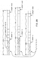
In Fig. 8, a pair of waveforms 100 and 101
respectively show the signals UP and SAMPLE. For each UP
pulse in waveform 100, two SAMPLE pulses occur in
waveform 101. This high pulse rate in the SAMPLE signal
insures that component 82 will sense each "1" that is set
in the flip-flop 81, even if the oscillator 78 is running
fast due to its frequency tolerance Δ2.
Further in Fig. 8, two examples of the down
pulses DN are shown by waveforms 102a and 102b. Waveform
102a occurs when the crystal oscillator 78 has a positive
tolerance Δ1 and thus the clock signal BYCKo has a faster
than nominal frequency. By comparison, waveform 102b
occurs when the crystal oscillator 78 has a negative
tolerance Δ1, and thus the clock signal BYCKo has a slower
than nominal frequency.
In waveform 102a, the first (left-most) down
pulse DN occurs simultaneously with the first (left-most)
UP pulse in waveform 101. Due to this simultaneous
occurrence of the DN pulse and UP pulse, count Co in the
counter 82 remains unchanged. Likewise, the second and
third down pulses DN in waveform 102a occurs
simultaneously with respective UP pulses in waveform 100.
By comparison, the fourth DN pulse in waveform
102a occurs by itself with no corresponding UP pulse in
waveform 100. consequently, count Co in the counter 82 is
decremented by "1"; and this indicates that the output
oscillator 78 is running faster than the nominal
frequency. Thereafter, the count in counter 78 switches
back and forth between two counts of C0 and C0-1 in
response to the UP and down DN pulses as shown. That
operation continues for many data blocks in accordance
with the normal header per long header ratios that were
previously described in conjunction with column 39 of
Fig. 3. But eventually, since the crystal oscillator 78
is running fast, another down DN pulse will be generated
with no corresponding UP pulse.
In waveform 102b, the first two down pulses DN
occur simultaneously with corresponding UP pulses
occurring in waveform 100; and consequently, the count C0
in counter 82 remains unchanged. But then, the third UP
pulse occurs in waveform 100 with no corresponding down
pulse in waveform 102b. Consequently, the count in
counter 83 is incremented by "1"; and this indicates that
the crystal oscillator 78 is oscillating at slower than
nominal frequency. Thereafter, the count in counter 82
switches back and forth between the count of C0+1 and C0
as shown in Fig. 8; and this operation continues to occur
for many data blocks in accordance with the normal header
per short header ratios of column 39 in Fig. 3. However,
since the oscillator 78 is running slow, the situation
will again eventually arise where an UP pulse is
generated with no corresponding down pulse.
In response to the count signal CNT from
counter 82 and the bytes which are received from register
71, control circuit 83 loads either a normal header, a
short header, or a long header into the FIFO 75 as shown
in Fig. 9. This figure is in the form of a table which
has three columns 110, 111, and 112. Column 110 shows
the type of header which is received by control circuit
83 from register 71; and column 111 shows the
corresponding count which is received by control circuit
83 from the counter 82. Based on those two inputs,
control circuit 83 loads the header which is shown in
column 112 into the FIFO 75.
For example, the top-most row in Fig. 9
indicates that when a normal header NH is received from
register 1 by control circuit 83 while the count CNT from
counter 82 is within a predetermined range PR, the
control circuit 83 loads a normal header NH into the FIFO
75. By comparison, the fourth row from the top of the
Fig. 9 table shows that when a normal header NH is
received from register 1 while the count CNT is greater
than the predetermined range, the control circuit 83
loads a short header SH into the FIFO 75. Conversely, the
seventh row from the top of the Fig. 9 table indicates
that when a normal header NH is received from register 1
while the count from the counter 82 is less than the
predetermined range PR, the control circuit 83 loads a
long header LH into the FIFO 75.
Inspection of the Fig. 9 table shows that the
operation of the control circuit 83 can be summarized as
follows. When a header is received from register 71
while the count CMT is greater than the predetermined
range, a corresponding header which is shorter by one
byte is generated in the FIFO 75, unless a short header
was received. When a header is received from register 71
while the count from counter 82 is less than the
predetermined range, a corresponding header which is
longer by one byte is generated in the FIFO 75, unless a
long header was received. In all other cases, the header
which is received from register 71 is duplicated in the
FIFO 75. This operation by the control circuit 83 is
identified in Fig. 9 by reference numerals 115a, 115b,
and 115c.
Preferably, before a header with a decreased
length or an increased length is stored in the FIFO 75,
the control circuit 83 checks the count which is received
from counter 82 for several consecutive headers. For
example, control circuit 83 can check the count which is
received from counter 82 for twenty consecutive headers.
Then, if the count for a large percentage (e.g. - 75%) of
those headers is greater than the predetermined range,
the action indicated by reference numeral 115a is taken;
and if the count for a large percentage (e.g. 75%) of
those headers is less than the predetermined range, the
action indicated by reference numeral 115b is taken. By
this means, any transient fluctuations in the count
signal CNT from the counter 83 will not cause unnecessary
length changes between the headers that are transmitted
and received.
Next, with reference to Fig. 10, a circuit
which constitutes one preferred embodiment of the
receiver 15 will be described. This Fig. 10 embodiment
includes several circuit components, and each component
is described below in TABLE 3.
| (Receiver Components) |
| ITEM | DESCRIPTION | |
| 120 | Component 120 is a serial-in, parallel-out register which as a serial input 120a, a byte-wide parallel output 120b, and a clock input 120c. On the rising edge of each clock pulse that is received on input 120c, one bit is loaded into register 120 from the input terminal 120a, and the last seven bits which were previously loaded from input 120a are shifted within register 120 by one bit position. |
| 121 122,& 123 | Each of the components 121, 122 and 123 is a one byte register. Each register has a byte-wide input, a byte-wide output, and a clock input. One byte is loaded into each register when the rising edge of a clock pulse occurs on the clock input. |
| 124 | Component 124 is a dual port, first-in, first-out, memory ("FIFO"). Memory 124 has a byte-wide input port 124a, a write control input 124b, and a byte-wide output port 124c, and a read control input 124d. One byte is loaded into memory 124 each time the rising edge of a pulse is received on input 124b. All bytes which are loaded into the memory 124 travel within the memory to the output port 124c in the same order in which they are loaded. A different byte is sent to the output port 124c each time the rising edge of a pulse occurs on the input 124d. Memory 124 holds a total of thirty-two bytes. |
| 125 | Component 125 is a descrambler which has a byte-wide input and a byte-wide output. On each byte that is received, component 125 performs a descrambling operation which is the inverse of the scrambling operation that is performed by component 43 in the Fig. 4 transmitter 10; and the result occurs on the output of component 125. |
| 126 | Component 126 is a parallel-in, serial-out register which has a byte-wide parallel input 126a, a serial output 126b, a clock input 126c, and a load control input 126d. One byte is loaded into register 126 each time the rising edge of a clock pulse occurs on input 126c while a LD signal on input 126b is true. That byte is shifted within register 126 by one bit position to the output terminal 126b each time a clock pulse occurs on input 126c while the LD signal is false. |
| 127 | Component 127 is phase locked oscillator (PLO) which has an input 127a, and two outputs 127b and 127c. Input 127a receives the continuous input series of data bits S4; and the phase locked oscillator 127 internally has a phase locked loop which locks on to that input series of bits S4. By locking on to the S4 bit series, oscillator 127 is able to generate a clock signal CKi on the output 127b which oscillates at nearly the same bit rate as the bit rate BR4 of the input bit series S4. Oscillator 127 also searches for the code C1 C2 C3 that occurs in each of the headers; and it generates a byte clock BYCKi on output 127c which is synchronized with that code and occurs once for every eight cycles of the bit clock CKi. |
| 128 | Component 128 is a voltage controlled oscillator (VCO) which has one input 128a and one output 128b. Input 128a receives an analog control voltage Vc; and in response. oscillator 128 generates a clock CKo on output 128b. As the magnitude of the analog control voltage increases, the frequency of clock CKo increases; and vice-versa. |
| 129 | Component 129 is a pulse generator which has two inputs 129a and 129b, and two outputs 129c and 129d. Input 129a receives a clock signal CKo and input 129b receives an enable control signal EN. When the EN signal is false, the outputs 129c and 129d are at a constant "0." When the EN signal is true, output 129c generates down pulses DN which occur at one-eighth the frequency of the clock signal CKo. Each pulse DN lasts for one cycle of clock CKo, and during the next cycle of clock CKo, a load pulse LD is generated on output 129d. |
| 130 | Component 130 is a counter which has two inputs 130a and 130b, and one output 130c. Each time an UP pulse is received on the input 130a, the counter 130 counts up by one; and each time a DOWN pulse is received on the input 130b, the counter 130 counts down by one. Output 130c provides the net result of this up and down counting as the signal CNT. Also, logic circuitry is incorporated into the counter 130 which stops the count CNT from rolling over past a count of zero and past a maximum count. |
| 131 | Component 131 is a count analyzer which has two inputs 131a, and 131b which respectively receive the count signal CNT from counter 130, and a control signal HDR. In response to these two input signals, component 131 generates speed-up pulses SUP and slow-down pulses SDN on an output 131c, and these pulses respectively cause the analog control voltage Vc for the VCO 128 to increase or decrease. When no pulses SUP or SDN are being generated, output 131c is in a high impedance state which approximates an open circuit. |
| 132 | Component 132 is a low pass filter which has an input which receives the speed-up pulses SUP and slow-down pulses SDN; and which filters those pulses to thereby generate the analog control voltage Vc for the VCO 128. |
| 133 & 134 | Component 133 is a digital inverter, and component 134 is a two input digital AND gate. These two components, together generate the UP pulses for the counter 130 and the FIFO 124. When the control signal HDR is true, inverter 133 inhibits the clock BYCKi from passing through AND gate 134; and consequently, the UP pulses are a constant "0." When the control signal HDR is false, the clock BYCKi passes through the AND gate 133 to thereby generate the UP pulses. |
| 135 | Component 135 is a sequential control circuit which has two inputs 135a and 135b, and two outputs 135c and 135d. Input 135a receives each byte which is held in register 121; and input 135b receives the byte clock BYCKi from the phase locked oscillator 127. In response to these two inputs, control circuit 135 generates the HDR signal on output 135c. Control signal HDR goes true when the first byte of a header is in register 123, and it goes false when the first byte of a data block is in register 123. Control signal HDR is generated within the control circuit 135 by examining the bytes which are received from register 121 to detect the predetermined code C1 C2 C3 which indicates the start of a header, and by examining the next byte which follows that code to determined the length of the header. Control circuit 135 also generates the enable signal EN on output 135d. When the EN signal is false, no down pulses DN are generated by the pulse generator 129; and consequently, no bytes are removed from the FIFO 124. Control circuit 135 generates the EN signal in a false state to initially fill the FIFO 124 half way. Thereafter, control circuit 135 always generates the EN control signal in a true state. |
All of the components 120-135 within the
receiver 15 are intercoupled to each other as shown in
Fig. 10; and how those components interact with each
other will now be described. From input terminal 15a,
the bit series S4 travels one bit at a time to register
120; and from there the bits are transferred one byte at
a time through registers 121, 122, and 123. Each byte
that is loaded into register 121 is examined by the
sequential control circuit 135 to determine if a header
is being received.
While register 123 holds the first byte of a
header, control circuit 135 generates the HDR signal in a
true state on output 135c; and that state is maintained
until register 123 holds the first byte of a data block.
When the HDR signal is true, components 133 and 134
prevent the UP pulses from occurring; and consequently,
the header bytes in the input series of bits S4 are not
loaded into the FIFO 124. Conversely, when the HDR
signal in a false state, each pulse of the byte clock
BYCKi passes through AND gate 134 to thereby generate a
corresponding UP pulse. Each UP pulse loads one data
byte from register 123 into the FIFO 124 and increments
the count CNT in the counter 130 by one.
In response to each down pulse DN from the
pulse generator 129, a new data byte is transferred
within the FIFO 124 to the output port 124c where it is
descrambled by component 125; and in addition, the count
CNT from the counter 130 is decremented by one. Then, in
response to each load pulse LD from the pulse generator
129, one byte of data is transferred from the descrambler
125 into the parallel-in, serial-out register 125. That
byte is then shifted bit by bit to the output terminal
15b.
From the counter 130, the count signals CNT are
sent to the count analyzer 131 which checks to see if the
count is within a predetermined range. If the maximum
count CNT gets so large that it goes outside of the
predetermined range, the count analyzer 131 generates
speed-up pulses SUP on output 131c such that the analog
control voltage Vc for the VCO 128 is slightly increased.
Conversely, if the minimum count CNT falls below the
predetermined range, then the count analyzer 131
generates slow down pulses SDN on output 131c such that
the analog control voltage Vc for the VCO is slightly
decreased.
Clock signal CKo from the VCO 128 increases in
frequency as the analog control voltage Vc is increased;
and vice-versa. By slightly increasing the frequency of
the clock signal CKo, a few more down pulses DN from by
the pulse generator 129 occur; and thus the maximum count
from the counter 130 slowly decreases. Conversely, by
slightly decreasing the frequency of the clock signal CKo,
a few less down pulses DN from the pulse generator 129
occur; and thus the minimum count from the counter 130
slowly increases.
A timing diagram which illustrates the above-described
operation of the Fig. 10 receiver is shown in
Fig. 11. There, waveform 140 shows the content of
register 121; waveform 141 shows the output from the FIFO
124; and waveform 142 shows the count CNT from the
counter 130.
Initially in Fig. 11, register 121 receives a
normal header NH followed by a data block DBi; then
register 121 receives a long header LH followed by a data
block DBi-1; and then register 121 receives a normal header
NH followed by a data block DBi+2. Due to the operation of
the control circuit 135, all of the data blocks but none
of the headers are loaded into the FIFO 124.
Consequently, in the FIFO output as shown by waveform
141, only the data blocks occur.
During the time periods that the headers are
being received, the counter 130 does not receive any UP
pulses but it does receive DN pulses. Thus when the
headers are being received, the counter 130 counts down;
and this occurs in waveform 142 during the time intervals
143a-143d. Each time interval 143a, 143c, and 143d
corresponds to the receipt of a normal header NH which is
five bytes long; and consequently, during those time
intervals, the counter 130 is decremented five times. By
comparison, time interval 143b corresponds to the receipt
of a long header which is six bytes long; and
consequently during time interval 143b, the counter 130
is decremented six times.
Between the time intervals 143a-143d, the bytes
of the data blocks DB are loaded into the FIFO 124 and
removed therefrom. Thus, between the time intervals
143a-143d, counter 130 is both incremented and
decremented. However, due to the operation of the
components 128-132, the rate at which data bytes are
removed from the FIFO 124 is slower than the rate at
which the data bytes are loaded into the FIFO. Thus,
between the time intervals 143a-143d, the count CNT in
counter 130 gradually increases. This increase, together
with the count decrease which occurs during the time
intervals 143a-143d give the count waveform 142 a
sawtooth shape.
Inspection of the sawtooth shaped waveform 142
in Fig. 11 shows that the CNT signal reaches a maximum
when the header is just starting to be received; and the
CNT signal reaches a minimum when the data blocks are
just starting to be received. Consequently, the maximum
count signal is sensed within the count analyzer 131 by
sampling the count CNT when the header signal HDR
switches from false to true, and the minimum count signal
is sensed by sampling the count CNT when the header
signal HDR switches from true to false.
If the minimum count which is sensed by the
count analyzer 131 lies below the predetermined range PR,
then the count analyzer 131 generates the slow down
pulses SDN such that the frequency of the clock signal CKo
from the voltage control oscillator 128 is decreased by
just a few cycles per second. Due to this slight decrease
in frequency, the minimum count will slowly rise such
that after several dozen data blocks DB pass through the
FIFO 124, the minimum count will again be back within the
predetermined range PR. This slow increase in the
minimum count indicated in Fig. 11 by reference numeral
150.
Similarly, if the maximum count which is sensed
by the count analyzer 131 lies outside above the
predetermined range PR, then the count analyzer 131
responds by generating the speed up pulses SUP such that
the frequency of the clock signal CKo from the VCO is
increased by just a few cycles per second. As a result,
the maximum count will slowly decrease; and after several
dozen data blocks DB pass through the FIFO, the maximum
count will again be within the predetermined range.
From the above it follows that the VCO 128, the
pulse generator 129, the counter 130, the count analyzer
131, and the low pass filter 132 together form a closed
loop feedback circuit. This loop automatically selects
the frequency of the clock signal CKo such that the count
CNT from the counter 130 stays within the predetermined
range PR. Consequently, the output series of bits SR is
continuous even though the headers were stripped from the
input series of bits S4.
Further, the closed loop feedback circuit 128-132
maintains the count CNT as a sawtooth shaped waveform
with a substantially constant average value NA.
Consequently, the bit rate of the clock signal CKo is
constant and automatically matches the bit rate of the
original series of bits Si which occur at the input of the
transmitter 10. Thus, the output series of bits SR from
the receiver 15 essentially duplicates the input series
of bits Si to the transmitter 10.
It should be pointed out that during initial
startup, hundreds of bytes may pass through the FIFO 124
before the clock CKo from the VCO 128 stabilizes at a
substantially constant frequency. This is because the
speed-up pulses SUP and slow down pulses SDN only make
small changes to the frequency of the clock CKo to thereby
minimize jitter. Preferably, the SUP and SDN pulses
change the frequency of the clock CKo by increments of
less than five-hundred parts per billion, with a total
adjustment range of one hundred parts per million.
To ensure that this slowly changing clock CKo
will eventually reach the proper constant frequency, the
counter 130 incorporates logic circuitry which prevents
the count CNT from rolling over. If the count CNT is
allowed to roll past zero, the slow down pulses SDN would
then switch to speed up pulses SUP; and if the count CNT
is allowed to roll past a maximum count, the speed up
pulses SUP would then switch to slow down pulses SDN.
One preferred embodiment of the present
invention has now been described in detail. In addition,
however, many changes and modifications can be made to
the details from this preferred embodiment without
departing from the nature and spirit of the invention;
and some of those modifications will now be described.
One modification is shown in Fig. 12 wherein
the continuous input series of data bits Si, which occurs
on input terminal 10a of the transmitter 10, consists of
'digital samples of speech. These digital samples of
speech are generated by a microphone 150, a sample and
hold circuit 151, and an analog-to-digital converter 152
which are serially intercoupled to each other as shown in
Fig. 12.
As another modification, the continuous input
series of data bits Si which occurs on input terminal 10a
of the transmitter 10 consists of pixels in successive
video frames. These pixels are generated by a camera
160, a sample and hold circuit 161, and an analog-to-digital
converter 162 which are serially intercoupled to
each other as shown in Fig. 13.
As another modification, the bit serial
communication channels 20-24 which intercouple the
transmitter 10, the repeaters 11-14, and the receiver 15
to each other, can be optical channels, wireless
channels, or electrical channels. In Fig. 14, the
illustrated channel is comprised of a voltage-to-optical
converter 170, an optical fibre 171, and an optical-to-voltage
converter 172 which are serially intercoupled.
In Fig. 15, illustrated channel is comprised of a
modulator 180, a transmitting antenna 181, a wireless
communication media 182, (such as air or space), a
receiving antenna 182, and a demodulator 183, all of
which are serially intercoupled. In Fig. 16, the
illustrated channel is comprised of a co-axial cable 190.
As another modification, the transmitter 10 can
be changed such that it receives a continuous stream of
data bits which consists of multiple input series of bits
that occur simultaneously in a bit-parallel fashion; and
the receiver 15 can also be changed such that it
duplicates those same bit series in an output stream from
the receiver. This modification will now be described in
conjunction with Figs 17 and 18.
Fig. 17 shows the input portion of a
transmitter which is a modification to the transmitter of
Fig. 4. In the Fig. 17 transmitter, the continuous input
series of data bits Si is again received on input terminal
10a; and simultaneously, another continuous input series
of data bits Si' is received on another input terminal
10a'. Input bit series Si is partitioned into groups of
four bits by a four bit wide serial-parallel register
40a'. Simultaneously, the bit series Si' is partitioned
into groups of four bits by a similar register 40b'.
From the registers 40a' and 40b', two groups of
four bits each are loaded in parallel into the register
41 where they form one byte. This loading of register 41
occurs once for every four cycles of the input bit clock
CKi which is generated by the phased-locked oscillator 46.
Each time a new byte is loaded into register 41, the
preceding byte is loaded into FIFO 42 and the counter 48
is incremented by one. All remaining circuitry within
the Fig. 17 transmitter is the same as components 43, 44,
45, 49, 50, 51, 52 and 53 in the Fig. 4 transmitter.
Similarly, Fig. 18 shows the output portion of
a receiver which is a modification to the Fig. 10
receiver. In the Fig. 18 receiver, bytes are loaded into
the FIFO 124 in the same manner that bytes are loaded
into the FIFO 124 of Fig. 10 receiver by components 120,
121, 122, 123, 127, 133, 134 and 135. Then, from the
output of the descrambler 125 in the Fig. 18 receiver,
each byte is partitioned into two groups of four bits
each. One four-bit group is loaded into a four bit wide
parallel-in, serial-out register 126a', while the other
four-bit group is simultaneously loaded into similar
register 126b'. That loading of the registers 126a' and
126b' occurs once for each four cycles of the output bit
clock CKo which is generated by the VCO 128, since the
pulse generator circuit 129' generates the down pulses DN
and the load pulses LD once for every four cycles of the
bit clock CKo.
All of the bits which are loaded into register
126a' are shifted bit-by-bit to the output terminal 15b
where they form the bit series SR. Simultaneously, all of
the bits which are loaded into the register 126b' are
shifted bit-by-bit to another output terminal 15b' where
they form an output bit series SR'. Bit series SR
essentially duplicates the input series of bits Si which
occurs as an input to the Fig. 17 receiver; and bit
series SR' essentially duplicates the bit series Si' which
occurs as another simultaneous input to the Fig. 17
transmitter.
As another modification, each of the headers
which are sent from the transmitter 10 and the repeaters
11-14 can be changed to include a field which indicates
the number of bytes that occur in the immediately
following data block. An example of this modification is
shown in Fig. 19, wherein the normal header NH includes a
four-byte number N1N2N3N4 which equals the total number of
bytes in the immediately following data block DB. With
this modification, the number of bytes which are in a
data block can vary from one data block to another.
To implement this Fig. 19 modification, the
transmitter of Fig. 4 generates the number N1N2N3N4 as part
of the header bytes HB which are sent from the sequential
control circuit 53 to the multiplexer 44; and that number
is also loaded into the DB counter 51. Then, within each
repeater of Fig. 6, the number N1N2N3N4 passes from
register 71 through the sequential control circuit 83 to
the multiplexer 74; and circuit 83 allows the following
data block of N1N2N3N4 bytes to go into the FIFO 75.
Thereafter, within the receiver of Fig. 10, the number
N1N2N3N4 is sent from register 121 to the sequential
control circuit 135; and in response to that number, the
sequential control circuit 135 generates the HDR signal
in a false state for a total of N1N2N3N4 bytes.
As another modification, the number of dummy
bits which are in a normal header NH and a long header LH
can respectively be any number X and 2X; where X
preferably is an integer which ranges from 1-64. This
modification is shown in Fig. 20 wherein each square
represents a group of X bits rather an eight-bit byte.
Thus, the normal header NH contains X dummy bits, the
long header LH contains 2X dummy bits, the control code
C1C2C3 is three groups of X bits, and the data block DB is
several consecutive groups of X bits each.
To implement this modification in the Fig. 4
transmitter, all of the components 40 through 45 are
changed to be X bits wide rather than one byte wide;
counter 47 becomes a divide by X counter; and pulse
generator 50 generates the LD pulse and BYCKo pulse once
for every X cycles of the clock CKo. Similarly to
implement this modification in the Fig. 6 repeater, all
of the components 70 through 76 are changed to be X bits
wide rather than one byte wide; phase locked loop 77
generates the clock BYCKi once for every X cycles of the
bit clock BYCKi; and the pulse generator 79 generates the
LD pulse and BYCKo pulse once for every X cycles of the
clock CKo. Likewise to implement this modification in the
Fig. 10 receiver, all of the components 120 through 126
are changed to be X bits wide rather than one byte wide;
the phase locked oscillator 127 generates the BYCKi pulses
once for every X cycles of the clock CKi; and pulse
generator 129 generates the LD pulse and DN pulse once
for every X cycles of the clock CKo.
As another modification, the dual port FIFO
which is included in the transmitter 10, the repeaters
11-14, and the receiver 15 can have practically any
desired storage capacity. However, due to the manner in
which the count CNT in the transmitter, the repeaters,
and the receiver, is kept within a predetermined range, a
FIFO with a large storage capacity is not needed; and
that in turn reduces the corresponding cost of the FIFO.
Thus, the FIFO within the transmitter, the repeaters, and
the receiver, preferably has a storage capacity of less
than 64 bytes.
As another modification, the data processing
system of Fig. 1 can be modified to include multiple
receivers 15, each of which have an input terminal 15a
that is coupled to one of the channels 20-24. In such a
system, all of those receivers can regenerate the
transmitter input series of data bits Si on their output
terminal 15b in the same manner as the previously
described receiver 15 of Fig. 10. Alternatively, the
headers which are sent from the transmitter 10 and the
repeaters 11-14 can be changed to include a field which
indicates that the immediately following data block is to
be received by only a particular one of the receivers;
and this modification is shown in Fig. 21. There, each
of the headers includes a field "R" which identifies one
particular receiver that is to receiver the immediately
following data block DB.
To implement 'this modification, the Fig. 10
receiver is changed such that the sequential control
circuit 135 examines the field R in each header as it is
held in register 121. If that field R matches a
particular number which is assigned to the receiver, the
control circuit 135 generates the header signal HDR in a
false state to pass the immediately following data block
DB into the FIFO 124. Otherwise, if a mismatch occurs,
the sequential control circuit 135 keeps the header
signal HDR in a true state while the immediately
following data block DB passes through register 123. To
allow for the irregular manner in which data is loaded
into the FIFO 124, the storage capacity of that FIFO and
the predetermined range PR may have to be increased to
more than 64 bytes.
As another modification, the headers which are
sent from the transmitter 10 and the repeaters 11-14 can
be modified to include fields which identifies certain
portions of each data block which are to be received by
the various receivers. An example of this modification
is shown in Fig. 22. There, the field S1S1S1 specifies
the number of the byte in the immediately following data
block at which the receiver R1 starts its receiving
operation; and the field E1E1E1 specifies the number of the
byte in the data block at which the receiver R1 ends its
receiving operation. Similarly, the field S2S2S2
specifies the number of the byte in the immediately
following data block DB at which the receiver R2 starts
its receiving operation and the field E2E2E2 specifies the
number of the byte in the data block at which the
receiver R2 ends its receiving operation.
To implement this modification, the Fig. 10
receiver is changed such that the sequential control
circuit 135 monitors the header characters as they are
held in register 121. If a match is found between the
header field R1 and a number which is assigned to the
receiver, then the sequential control circuit 135
generates the header signal HDR in a false state while
the characters #S1S1S1 through #E1E1E1 of the immediately
following data block DB are held in register 123.
Similarly, if the sequential control circuit 135 finds a
match between the, header field R2 and a number which is
assigned to the receiver, then the sequential control
circuit 135 generates the header signal HDR in a false
state while the characters #S2S2S2 through #E2E2E2 are held
in register 123. Here again, to allow for the irregular
manner in which data is loaded into the FIFO 124, the
storage capacity of that FIFO and the predetermined range
PR may have to be increased to more than 64 bytes.
With the above two modifications of Figs. 21
and 22, the output series of bits SR from the Fig. 10
receiver will still be continuous and the bit rate BRR
will still be substantially constant. This result occurs
due to the operation of the closed loop feedback control
circuit which is formed by components 128-132 in the Fig.
10 receiver. However, the receiver output bit rate BRR
will no longer equal the transmitter input bit rate BRi.
Instead, bit rate BRR will equal the one particular
constant rate which keeps the count CNT from the counter
130 within the predetermined range PR.
As another modification, the digital
communication system of Fig. 1 can be modified such that
any number of repeaters serially interconnect the
transmitter 10 to the receiver 15. Alternatively, the
Fig. 1 digital communication system can be modified such
that the transmitter 10 is connected directly to the
receiver 15 with no repeaters there between.
As another modification, the independent
oscillator 49 within the transmitter 10 and the
independent oscillator 78 within the repeaters 11-14 need
not be a crystal oscillator. Instead, those oscillators
49 and 78 can be any oscillator that generates highly
stable clock signals independent of the phased-locked
oscillators 46 and 77 which also are in the transmitter
and the repeaters respectively. For example, the
oscillators 49 and 78 can be a Cesium atomic clock, or a
ceramic resonator.
As another modification, the sequential control
circuits 53, 83, 135, which are respectively in the
Fig. 4 transmitter, the Fig. 6 repeater, and the Fig. 10
receiver can be implemented as a special purpose
sequential state machine, or a programmable
microprocessor.
Accordingly, since many such modifications can
be made to the details of the illustrated preferred
embodiments, it is to be understood that the present
invention is not limited to those details, but is defined
by the appended claims.