EP0902413A2 - Image drawing apparatus - Google Patents
Image drawing apparatus Download PDFInfo
- Publication number
- EP0902413A2 EP0902413A2 EP98307388A EP98307388A EP0902413A2 EP 0902413 A2 EP0902413 A2 EP 0902413A2 EP 98307388 A EP98307388 A EP 98307388A EP 98307388 A EP98307388 A EP 98307388A EP 0902413 A2 EP0902413 A2 EP 0902413A2
- Authority
- EP
- European Patent Office
- Prior art keywords
- buffer
- circuit
- dimensional
- frame buffer
- data
- Prior art date
- Legal status (The legal status is an assumption and is not a legal conclusion. Google has not performed a legal analysis and makes no representation as to the accuracy of the status listed.)
- Withdrawn
Links
Images


Classifications
-
- G—PHYSICS
- G06—COMPUTING OR CALCULATING; COUNTING
- G06T—IMAGE DATA PROCESSING OR GENERATION, IN GENERAL
- G06T15/00—Three-dimensional [3D] image rendering
- G06T15/10—Geometric effects
- G06T15/40—Hidden part removal
- G06T15/405—Hidden part removal using Z-buffer
-
- G—PHYSICS
- G09—EDUCATION; CRYPTOGRAPHY; DISPLAY; ADVERTISING; SEALS
- G09G—ARRANGEMENTS OR CIRCUITS FOR CONTROL OF INDICATING DEVICES USING STATIC MEANS TO PRESENT VARIABLE INFORMATION
- G09G5/00—Control arrangements or circuits for visual indicators common to cathode-ray tube indicators and other visual indicators
- G09G5/36—Control arrangements or circuits for visual indicators common to cathode-ray tube indicators and other visual indicators characterised by the display of a graphic pattern, e.g. using an all-points-addressable [APA] memory
- G09G5/39—Control of the bit-mapped memory
- G09G5/393—Arrangements for updating the contents of the bit-mapped memory
-
- G—PHYSICS
- G09—EDUCATION; CRYPTOGRAPHY; DISPLAY; ADVERTISING; SEALS
- G09G—ARRANGEMENTS OR CIRCUITS FOR CONTROL OF INDICATING DEVICES USING STATIC MEANS TO PRESENT VARIABLE INFORMATION
- G09G2360/00—Aspects of the architecture of display systems
- G09G2360/12—Frame memory handling
-
- G—PHYSICS
- G09—EDUCATION; CRYPTOGRAPHY; DISPLAY; ADVERTISING; SEALS
- G09G—ARRANGEMENTS OR CIRCUITS FOR CONTROL OF INDICATING DEVICES USING STATIC MEANS TO PRESENT VARIABLE INFORMATION
- G09G5/00—Control arrangements or circuits for visual indicators common to cathode-ray tube indicators and other visual indicators
- G09G5/36—Control arrangements or circuits for visual indicators common to cathode-ray tube indicators and other visual indicators characterised by the display of a graphic pattern, e.g. using an all-points-addressable [APA] memory
- G09G5/39—Control of the bit-mapped memory
Definitions
- This invention concerns an image drawing apparatus that can perform three-dimensional drawing on a display screen of a display apparatus.
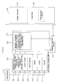
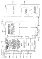
- Fig. 12 is a block diagram representing an example configuration of a known image drawing apparatus.
- This image drawing apparatus comprises: a CRT 10 for displaying images; a frame buffer 12 for storing display data corresponding to the display screen of the CRT 10; a two-dimensional drawing circuit 14 for drawing desired rectangular images, etc., to the frame buffer 12; a Z buffer 16 for storing depth data (Z values) for performing three-dimensional drawing to the frame buffer 12; a three-dimensional straight line drawing circuit 18 for performing three-dimensional drawing to the frame buffer 12 based on the depth data stored in the Z buffer 16; a Z buffer setting circuit 20 for setting desired rectangular area data, etc., in the Z buffer 16; a processor 22 for performing overall control of the image drawing apparatus; and a main memory 24 for providing the processor 22 with a control program and work area.
- the processor 22 first produces two-dimensional data in the main memory 24. These two-dimensional data may be configured of line segments (straight lines), for example. By writing these to the frame buffer 12, images are displayed on the CRT 10.
- the two-dimensional drawing circuit 14 is a dedicated circuit for writing certain two-dimensional images to the frame buffer 12 at high speed. More specifically, there are present a dedicated circuit for drawing two-dimensional straight lines, a dedicated circuit for filling in two-dimensional rectangular areas, and a dedicated circuit for transferring a two-dimensional rectangular area to another position.
- high-speed drawing is effected by regular coordinate operation actions responsive to the attributes of the two-dimensional images being drawn. This is effected by setting addresses for specifying the shapes and positions of two-dimensional images such as noted above, and, in conjunction therewith, setting drawing color data, etc.
- the Z buffer stores depth data (Z values) contained in pixels (XY coordinates) drawn in the frame buffer 12.
- the three-dimensional straight line drawing circuit 18 compares depth data (source Z values) for each point in the XY coordinates of three-dimensional straight lines input from the processor 22 against the depth data (destination Z values) stored beforehand in the Z buffer 16, selects the data having the smaller depth, and writes the data to the frame buffer 12.
- Fig. 13 is a block diagram representing the configuration of the three-dimensional straight line drawing circuit 18.
- This three-dimensional straight line drawing circuit 18 comprises: a register 102 for storing source Z values input from the processor 22; a comparator 104 for comparing source Z values stored in the register 102 against destination Z values stored in the Z buffer 16; a raster operation processor (ROP) circuit 106 for performing logical operations on the source values and on the data present originally in the frame buffer 12 using AND, OR, XOR, or other logic circuits; a straight line operation circuit 108 for drawing straight lines to the frame buffer 12 by providing coordinate parameters for the start point and end point of straight lines to be drawn; a transfer circuit 110 for rewriting the Z buffer 16 based on the results of comparator 104 operations; a frame buffer address operation circuit 112 for generating and controlling addresses for accessing the frame buffer 12; and a Z buffer address operation circuit for generating and controlling addresses for accessing the Z buffer 16.
- ROP raster operation processor
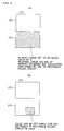
- Fig. 14 is an explanatory diagram for describing the Z buffer operation processing for drawing any vector (straight line).
- the Z value computed in this way is compared with the Z value of the pixel originally at those coordinates by the comparator 104.
- the Z buffer 16 If the newly computed Z value is smaller, the results of that computation are written to the Z buffer 16, writing the pixel to the frame buffer 12 is enabled, and a pixel is written based on the new drawing. If the newly computed Z value is larger, the Z buffer 16 and the frame memory 12 are kept the same (that is, the pixel there originally is retained).
- Z values are set one at a time at points in the area established. This not only makes high-speed processing very difficult, but also puts a large burden on the processor 22 that controls the whole system.
- the Z buffer setting circuit 20 is a dedicated circuit for writing specific two-dimensional images to the Z buffer 16 at high speed.
- high-speed setting is achieved by regular coordinate operation actions that are responsive to the attributes of the two-dimensional areas in which Z values are set.
- the two-dimensional drawing circuit 14 and the Z buffer setting circuit 20 described above have similar configurations in those parts that perform specific area coordinate operations, but are configured to handle attributes of the frame buffer 12 and Z buffer 16 that, respectively, are the objects of access, making it very difficult to use them interchangeably.
- the root cause of this difficulty lies in the fact that the number of bytes per pixel differs between the frame buffer 12 and the Z buffer 16.
- the number of bytes per pixel in the frame buffer 12 is determined according to the gradations of the color data stored in the frame buffer 12. With 255 gradations in each color component, for example, 1 byte of data is required per pixel for each color component. For four color components, therefore, 4 bytes (32 bits) are required.
- the number of bytes per pixel in the Z buffer 16 is determined by the depth resolution afforded by the Z value data. If the number of bytes per pixel is increased, it becomes possible, by that same measure, to draw three-dimensional images that are more complex in the depth dimension. Two bytes of Z value data per pixel are used, for example.
- the gradations of the color data stored in the frame buffer 12 and the resolution of the Z value data stored in the Z buffer 16 are usually different. Correspondingly, therefore, the configurations of these buffers also differ.
- An object of the present invention is to provide an image drawing apparatus wherewith the two-dimensional drawing circuit for the frame buffer can be used also as the setting circuit for the Z buffer, so that both Z buffer high-speed setting processing and cost reductions can be realized at one and the same time.
- an image drawing apparatus comprises: a frame buffer for storing display data corresponding to a display apparatus display screen; a two-dimensional drawing circuit for performing coordinate operations in order to draw specific two-dimensional images in the frame buffer; a Z buffer for storing depth data for performing three-dimensional drawing to the frame buffer; a three-dimensional straight line drawing circuit for performing three-dimensional drawing in the frame buffer, based on the depth data stored in the Z buffer; a memory control circuit for setting areas of the frame buffer and Z buffer in the same physical memory and also controlling access to each buffer; and a bit number altering circuit for changing the number of bits per pixel in the coordinate operations of the two-dimensional drawing circuit to either a number of bits corresponding to drawing data in the frame buffer or to a number of bits corresponding to the depth data in the Z buffer; wherein: drawing to the frame buffer and setting depth data in the Z buffer are conducted selectively by the coordinate operations of the two-dimensional drawing circuit.
- both frame buffer and Z buffer areas are established as appropriate in the same physical memory, and the two buffer areas are selectively accessed by the two-dimensional drawing circuit.
- this access is accomplished after altering, by the bit number altering circuit, the number of bits per pixel in the coordinate operations of the two-dimensional drawing circuit to a number of bits corresponding to the drawing data in the frame buffer. And when accessing the Z buffer from the two-dimensional drawing circuit, the number of bits per pixel in the coordinate operations of the two-dimensional drawing circuit are changed by the bit number altering circuit to the number of bits corresponding to the depth data in the Z buffer.
- drawing to the frame buffer and setting depth data in the Z buffer can be performed selectively by coordinate operations of the two-dimensional drawing circuit.
- the two-dimensional drawing circuit for the frame buffer can be used as the setting circuit for the Z buffer, and depth data can be set to the Z buffer at higher speed without providing a dedicated Z buffer setting circuit, thereby realizing both high-speed setting processing for the Z buffer and reduced costs.
- the Z buffer By giving the Z buffer the same configuration as the frame buffer, using a memory control circuit, it is possible to set two frame buffers of equal size and number of bits per pixel in the physical memory, to alternately perform drawing to each frame buffer without altering the number of bits using a bit number altering circuit, and thus to create a system wherein the frame buffers can be used as double buffers for animation.
- Fig. 1 is a block diagram of an image drawing apparatus based on a first embodiment of the present invention.
- This image drawing apparatus comprises: a CRT 210 for displaying images; a buffer memory 240 providing a frame buffer 220 for making displays on the CRT 210 and a Z buffer 230 for three-dimensional drawing; a two-dimensional drawing circuit 200 for drawing desired rectangular areas in the buffer memory 240 and making settings, etc.; a memory control circuit 250 for setting buffer areas for the buffer memory 240 and controlling access thereto; a three-dimensional straight line drawing circuit 260 for performing three-dimensional drawing to the frame buffer 220 based on Z value data stored in the Z buffer 230; a processor 270 for performing overall control of the image drawing apparatus; and a main memory 280 for providing a control program and work area for the processor 270.
- the three-dimensional straight line drawing circuit 260 draws three-dimensional straight lines to the frame buffer 220 using the principle diagrammed in Fig. 14.
- the processor 270 supplies the source Z values discussed earlier to the three-dimensional straight line drawing circuit 260.
- the three-dimensional straight line drawing circuit 260 compares the source Z values from the processor 270 against the destination Z values stored in the Z buffer 230 and, based on the results of such comparison, draws three-dimensional straight lines to the frame buffer 220.
- the frame buffer 220 and Z buffer 230 are provided in the buffer memory 240, that is, in the same physical memory, and the two-dimensional drawing circuit 200 can, by means of the memory control circuit 250, freely access both of the buffers 220 and 230.
- the frame buffer 220 has a size of 640 x 280 pixels, and stores 8 bits, 16 bits, or 32 bits of color data per pixel.
- the number of bits per pixel in the frame buffer 220 is determined by the color data gradations, as noted earlier.
- the color data gradations are determined by the application software or by operator input from a keyboard (not shown), etc.
- the lead address in the frame buffer 220 is 3000000h, where the h at the end indicates that this is a hexadecimal number.
- the Z buffer 230 here has a size of 640 x 480 pixels, set up so as to represent depths in terms of Z values that are either 16 or 32 bits per pixel.
- the number of bits per pixel in the Z buffer 230 is determined by the depth resolution provided by the Z value data, as noted earlier.
- the depth resolution provided by the Z value data is determined either by the application software or by operator input from a keyboard, etc.
- the lead address of the Z buffer 230 is 3004B00h.
- the two-dimensional drawing circuit 200 in this embodiment is configured to perform processing to fill in rectangular areas.
- It performs processing to fill in desired rectangular areas in the desired color for the frame buffer 220. It also sets Z values in the desired rectangular area for the Z buffer 230 and performs initializing processing, for example.
- Fig. 2 is a block diagram of the two-dimensional drawing circuit 200.
- the two-dimensional drawing circuit 200 comprises a register circuit 300 for setting various parameters for performing processing to fill in rectangular areas, and a memory address operation circuit 330 for performing address operations on the frame buffer 220 and Z buffer 230, based on the parameters set in the register circuit 300.
- the register circuit 300 comprises a drawing pixel-byte number setting register 302, a drawing lead address setting register 304, a start point setting register 306, a width-height register 308, a drawing mode setting register 310, a start setting register 312, and a color setting register 314.
- the setting of the various parameters for this register circuit 300 is done by the processor 270, prior to accessing the frame buffer 220 or Z buffer 230, based on operator inputs from the keyboard or the application software.
- the processor 270 when drawing rectangles to the frame buffer 220 or drawing rectangles (setting Z data) to the Z buffer 230, makes settings to change the drawing lead address or drawing pixel-byte number.
- the two-dimensional drawing circuit 200 computes addresses for drawing pixels of rectangular areas in the memory address operation circuit 330, based on the parameters set in the register circuit 300 described above, and outputs these addresses to the memory control circuit 250.
- the memory control circuit 250 accesses the frame buffer 220 or Z buffer 230, and writes Z value data or color data stored in the color setting register 314.
- data writing is performed using a number of bytes corresponding to the frame buffer 220 when that buffer is being accessed, and data writing is performed using a number of bytes corresponding to the Z buffer 230 when that buffer is being accessed.
- start point setting register 306 width-height register 308, drawing mode setting register 310, and start setting register 312
- start point setting register 306 width-height register 308
- drawing mode setting register 310 drawing mode setting register 310
- start setting register 312 start setting register
- the address operations in the memory address operation circuit 330 are performed synchronously with data writing actions in the memory control circuit 250, based on synchronous signals from the memory control circuit 250, for example.
- the two-dimensional drawing circuit 200 is now described in greater detail.
- Fig. 3 is an explanatory chart indicating specific examples of correlations between memory addresses and formats for the various setting registers in the register circuit 300 in this embodiment.
- the register circuit 300 in this embodiment has a data width of 32 bits, with a lead address, let it be assumed, of 2000000h in the register circuit 300.
- the drawing pixel-byte number setting register 302 configures a bit number altering circuit. This is a register that sets the number of bits per pixel, in byte units, when calculating addresses for rectangles, corresponding to the buffer 220 or 230 that is being accessed. If the number of bits per pixel is 8, 0h is set; if 16, 1h is set; and if 32, 2h is set.
- the drawing lead address setting register 304 sets the memory address for the origin (0, 0) in the system of coordinates wherein the rectangle being drawn is designated.
- the start point setting register 306 is a register that sets the pixel coordinates at the upper left point in a rectangle to be filled in, representing the Y coordinate by the higher 16 bits and the X coordinate by the lower 16 bits.
- the width-height register 308 sets data representing the width and height of a rectangle to be filled in, expressing the height by the higher 16 bits and the width by the lower 16 bits.
- rectangles are designated by the upper left point in the rectangle and the width and height of the rectangle.
- the drawing mode setting register 310 is a register that selects straight line drawing or rectangle drawing, setting lh when filling in a rectangle.
- the start setting register 312 is a register for designating the start of drawing. Drawing is initiated by setting a 1 in this register 312.
- the color setting register 314 is a register for setting rectangle fill colors and rectangle Z values, depending on the value set in the drawing pixel-byte setting register 302. If this value represents 8 bits (1 byte), 8-bit-based color data are set; if 16 bits (2 bytes), 16-bit-based color data or Z values are set; and if 32 bits (4 bytes), 32-bit-based color data or Z values are set.
- 0h is set in the color setting register 314, and 0-clearing data are written to each point.
- the necessity of clearing the Z buffer 230 arises frequently.
- the Z buffer 230 can be cleared fast. Because voluminous memory accesses are required for this clearing operation, the processing can be done at high speed using the two-dimensional drawing circuit 200.
- Fig. 4 (A) diagrams the situation wherein the entire Z buffer 230 has been cleared by 0h rectangular data corresponding to the entire area of the Z buffer 230.
- a window displayed on the CRT 210 screen can also be 0-cleared.
- rectangles can be designated by the method of designating coordinates (x, y) in the frame buffer 220 when filling them in on the frame buffer 220, and rectangles can be designated in a coordinate system (x, y) on the Z buffer 230 when filling them in on the Z buffer 230.
- the common two-dimensional drawing circuit 200 can be used even though the number of bytes per pixel differs between the frame buffer 220 and Z buffer 230.
- the memory address operation circuit 330 calculates addresses point by point for the pixels being drawn, based on the setting parameters in the register circuit 300 as described above.
- Fig. 5 is an explanatory diagram showing an example of settings in the color setting register 314 for the same rectangle in both the frame buffer 220 and Z buffer 230.
- Fig. 5 (A) diagrams a row of drawing data for the frame buffer 220. "ALPHA,” “RED,” “GREEN,” and “BLUE” data are set, designating the color to be filled in, in the color setting register 314.
- Fig. 5(B) diagrams a row of Z values for the Z buffer 230, setting "Z" as the Z value data.
- Fig. 6 diagrams the situation wherein a rectangular area is filled in, in the frame buffer 220, by the register settings shown in Fig. 5(A), and the situation wherein Z values are set in a rectangular area in the Z buffer 230 by the register settings indicated in Fig. 5(B).
- register 1. is the drawing lead address setting register 304
- register 2. is the drawing pixel-byte number setting register 302
- register 3. is the start point setting register 306
- register 4. is the width-height register 308, and register 5. is the color setting register 314.
- the two-dimensional drawing circuit 200 is configured so that it is normally held in a state wherein it stores display data by the frame buffer 220, so that it rewrites setting data temporarily to the Z buffer 230 only when making settings in the Z buffer 230, and so that it automatically rewrites data to the frame buffer 220 after completing the settings in the Z buffer 230.
- the drawing pixel-byte number setting register 302 of the two-dimensional drawing circuit 200 is temporarily set at 32 bits, and, after making settings to the Z buffer 230, the drawing pixel-byte number setting register 302 is changed to a value conforming to the frame buffer 220.
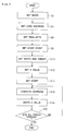
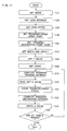
- Fig. 7 is a flowchart of the procedures for clearing the Z buffer 230.
- register circuit 300 settings are made by the processor 270. Initially, a value of lh is set in the drawing mode setting register 310 to designate the rectangle fill mode (step S2). Next, the drawing lead address setting register 304 is set to 3004B00h (step S4).
- the width-height register 308 is set to (width 640, height 480) (step S10).
- the entire area of the Z buffer 230 is designated here in order to clear the entire area of the Z buffer 230.
- drawing point addresses are calculated by the numerical formula noted below in the memory address operation circuit 330 of the two-dimensional drawing circuit 200, and these are sent to the memory control circuit 250 (step S16).
- DRAWING POINT ADDRESS LEAD ADDRESS + X COORDINATE ⁇ DRAWING PIXEL-BYTE NUMBER + Y COORDINATE ⁇ DRAWING PIXEL-BYTE NUMBER ⁇ NUMBER OF PIXELS IN 1 SCAN LINE
- the memory control circuit 250 writes the values of the color setting register 314 at the aforesaid addresses sent from the two-dimensional drawing circuit 200 (step S18).
- the memory address operation circuit 330 of the two-dimensional drawing circuit 200 calculates the next drawing point (step S16), references the drawing pixel-byte number, advances the address by the number of bytes per pixel, and writes the value in the color setting register 314 at the next drawing point (step S18).
- the address is advanced by the difference (number of bytes in scan line - number of bytes in rectangle width), and values are written for the drawing point on the next scan line.
- step S20 A determination is made (in step S20) as to whether or not the action described above has been executed for all of the pixels in the rectangular area. If this has not been finished, step S16 is returned to and steps S16 and S18 are executed.
- the Z buffer 230 can be cleared or rewritten using the two-dimensional drawing circuit 200 for the frame buffer 220, making it possible to realize high-speed Z buffer 230 settings in a low-cost configuration.
- the description pertains to the case where a rectangle filling circuit is adopted as the two-dimensional drawing circuit 200. In this embodiment, however, the description pertains to a case where a rectangle transfer circuit is adopted as the two-dimensional drawing circuit 200.
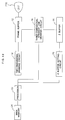
- Fig. 8 diagrams how drawing data in the frame buffer 220 and Z value data in the Z buffer 230 move in conjunction with the movement of such a window on the CRT screen.
- At (A) is represented a case where a three-dimensional application window moved from the upper left to the lower right on the CRT screen, at (B) a case where color value data for a rectangular area in the frame buffer 220 moved, and at (C) a case where Z value data for a rectangular area in the Z buffer 230 moved.
- the movement of rectangle data in the Z buffer is performed at high speed using the two-dimensional drawing circuit 200.
- Fig. 9 is a block diagram of the two-dimensional drawing circuit 200 in this embodiment.
- the register circuit 300 of the two-dimensional drawing circuit 200 is modified, in part, relative to the configuration diagrammed in Fig. 2.
- the two-dimensional drawing circuit 200 in this embodiment comprises a transfer-origin rectangle start point position setting register 320 for storing transfer-origin rectangle start point addresses, and a transfer-destination rectangle start point position setting register 322 for storing transfer-destination rectangle start point addresses.
- This embodiment also comprises a drawing pixel-byte number setting register 302, a drawing lead address setting register 304, a width-height register 308, a drawing mode setting register 310, a start setting register 312, and a color setting register 314, each have the same functions as in the embodiment diagrammed in Fig. 2.
- Fig. 10 is an explanatory diagram that provides specific examples of correlations between memory addresses and formats for the setting registers in the register circuit 300 in this embodiment.
- the transfer-origin rectangle starting point position setting register 320 stores the pixel coordinates for the upper left point in the transfer-origin rectangular area.
- the Y coordinate is stored in the higher 16 bits and the X coordinate in the lower 16 bits.
- the transfer-destination rectangle starting point position setting register 322 stores the pixel coordinates for the upper left point in the transfer-destination rectangular area.
- the Y coordinate is stored in the higher 16 bits and the X coordinate in the lower 16 bits.
- the transfer-destination rectangle position is described as (10, 70), the transfer rectangle width and height as (210, 50), and the transfer-destination rectangle position as (130, 200).
- the color setting register 314 in this embodiment stores the Z value set in an area after the transfer-origin rectangular area has been cleared by transferring [its contents]. In this example the color setting register 314 stores the value 0h.
- Fig. 11 is a flowchart for the procedures used when transferring [the contents of] the Z buffer 230.
- settings are made in the register circuit 300 by the processor 270.
- 2h is set in the drawing mode setting register 310 to designate the rectangle transfer mode (step S32).
- step S34 3004B00h is set in the drawing lead address setting register 304 (step S34) .
- 32 bpp 2h is set in the drawing pixel-byte number setting register 302 (step S36).
- DRAWING POINT ADDRESS LEAD ADDRESS + X COORDINATE ⁇ DRAWING PIXEL-BYTE NUMBER + Y COORDINATE x DRAWING PIXEL-BYTE NUMBER ⁇ NUMBER OF PIXELS IN 1 SCAN LINE
- the memory control circuit 250 reads out the Z value from the Z buffer 230 corresponding to the address sent from the two-dimensional drawing circuit 200 and stores it in a transfer register (not shown) (step S50). Then the value (0h) in the color setting register 314 is written at that address (step S52).
- step S48 the addresses of the drawing points in the transfer-destination rectangular area are computed and sent to the memory control circuit 250 (step S54).
- the memory control circuit 250 writes the Z value stored in the transfer register mentioned above at the address sent from the two-dimensional drawing circuit 200 (step S56).
- step S48 is returned to and the next drawing point is transferred. This action is executed for all of the pixels in the rectangular area (step S58).
- rectangular areas in the Z buffer 230 can be transferred using the two-dimensional drawing circuit 200 that is for the frame buffer 220, and hence the Z buffer 230 can be rewritten at high speed in a low-cost configuration.
- the Z buffer 230 is made to have the same size as the frame buffer 220 and the number of bits per pixel is made common to both, thus configuring a double buffer system having two frame buffers.
- This double buffer system is a display system for use in animation.
- the frame buffers displayed on the screen of the CRT 210 are changed alternately.
- the system can function as a double buffer system.
- the buffer memory 240 can be widely used in various applications, making it possible in particular to provide an effective apparatus that can support multimedia applications.
- the present invention can likewise be applied in cases where a two-dimensional drawing circuit for drawing two-dimensional straight lines is provided.
Landscapes
- Engineering & Computer Science (AREA)
- Physics & Mathematics (AREA)
- General Physics & Mathematics (AREA)
- Theoretical Computer Science (AREA)
- Computer Hardware Design (AREA)
- Geometry (AREA)
- Computer Graphics (AREA)
- Image Generation (AREA)
- Controls And Circuits For Display Device (AREA)
- Solid State Image Pick-Up Elements (AREA)
- Image Input (AREA)
Abstract
Description
Claims (10)
- A three-dimensional image drawing apparatus comprising:a frame buffer for storing display data corresponding to a display apparatus display screen;a two-dimensional drawing circuit for performing coordinate operations in order to draw specific two-dimensional images to said frame buffer;a Z buffer for storing depth data for performing three-dimensional drawing to said frame buffer;a three-dimensional straight line drawing circuit for performing three-dimensional drawing to said frame buffer based on said depth data stored in said Z buffer;a memory control circuit for controlling access to the buffers; anda bit number altering circuit for altering the number of bits per pixel in coordinate operations in said two-dimensional drawing circuit either to a number of bits corresponding to drawing data in said frame buffer or to a number of bits corresponding to depth data in said Z buffer; wherein:areas of said frame buffer and Z buffer are established in same physical memory; andsaid bit number altering circuit selectively performs drawing to said frame buffer and setting of depth data to said Z buffer by coordinate operations of said two-dimensional drawing circuit, by altering the number of bits per pixel in the coordinate operations of said two-dimensional drawing circuit.
- The image drawing apparatus according to Claim 1, wherein said bit number altering circuit alters the number of bits per pixel in byte units.
- The image drawing apparatus according to Claim 1, wherein said bit number altering circuit sets a number of bits corresponding either to said frame buffer or to said Z buffer in a bit number setting circuit that sets the number of bits per pixel and that is provided in said two-dimensional drawing circuit.
- The image drawing apparatus according to Claim 1, wherein said two-dimensional drawing circuit comprises an area setting circuit for setting drawing areas for specific figures, and selectively accesses either said frame buffer or said Z buffer, based on address of drawing area set in said area setting circuit.
- The image drawing apparatus according to Claim 4, wherein: said two-dimensional drawing circuit comprises: a bit number setting circuit for setting the number of bits per pixel; and a data setting circuit for setting data to be written into said specific figures; said two-dimensional drawing circuit stores a number of bits corresponding to said frame buffer in said bit number setting circuit and also stores color data in said data setting circuit, when drawing to said frame buffer; and said two-dimensional drawing circuit stores a number of bits corresponding to said Z buffer in said bit number setting circuit and also stores depth data in said data setting circuit, when making settings to said Z buffer.
- The image drawing apparatus according to Claim 1, wherein said two-dimensional drawing circuit draws two-dimensional straight lines.
- The image drawing apparatus according to claim 1, wherein said two-dimensional drawing circuit fills in two-dimensional rectangular areas.
- The image drawing apparatus according to Claim 1, wherein said two-dimensional drawing circuit transfers two-dimensional rectangular areas to other positions.
- The image drawing apparatus according to Claim 1, wherein said three-dimensional straight line drawing circuit compares depth data at points on three-dimensional straight lines input against depth data stored beforehand in said Z buffer, selects data having smaller depth, and rewrites data to said frame buffer.
- A three-dimensional image drawing apparatus comprising:a frame buffer for storing display data corresponding to a display apparatus display screen;a two-dimensional drawing circuit for performing coordinate operations in order to draw specific two-dimensional images to said frame buffer;a Z buffer for storing depth data for performing three-dimensional drawing to said frame buffer;a three-dimensional straight line drawing circuit for performing three-dimensional drawing in said frame buffer based on said depth data stored in said Z buffer; anda memory control circuit for controlling access to the buffers; wherein:areas of said frame buffer and Z buffer are established in same physical memory;said physical memory comprises two frame buffers having same size and same number of bits per pixel; andsaid memory control circuit uses said frame buffers as a double buffer for animation, by alternately drawing to said two frame buffers.
Applications Claiming Priority (3)
| Application Number | Priority Date | Filing Date | Title |
|---|---|---|---|
| JP9247073A JP2976945B2 (en) | 1997-09-11 | 1997-09-11 | Image drawing device |
| JP247073/97 | 1997-09-11 | ||
| JP24707397 | 1997-09-11 |
Publications (2)
| Publication Number | Publication Date |
|---|---|
| EP0902413A2 true EP0902413A2 (en) | 1999-03-17 |
| EP0902413A3 EP0902413A3 (en) | 2000-06-28 |
Family
ID=17158036
Family Applications (1)
| Application Number | Title | Priority Date | Filing Date |
|---|---|---|---|
| EP98307388A Withdrawn EP0902413A3 (en) | 1997-09-11 | 1998-09-11 | Image drawing apparatus |
Country Status (5)
| Country | Link |
|---|---|
| US (1) | US6275241B1 (en) |
| EP (1) | EP0902413A3 (en) |
| JP (1) | JP2976945B2 (en) |
| KR (1) | KR100281949B1 (en) |
| TW (2) | TW407306B (en) |
Cited By (1)
| Publication number | Priority date | Publication date | Assignee | Title |
|---|---|---|---|---|
| GB2352380A (en) * | 1999-03-01 | 2001-01-24 | Canon Kk | Random access video memory control |
Families Citing this family (14)
| Publication number | Priority date | Publication date | Assignee | Title |
|---|---|---|---|---|
| US6452600B1 (en) * | 1999-10-28 | 2002-09-17 | Nintendo Co., Ltd. | Graphics system interface |
| JP4519290B2 (en) * | 2000-08-04 | 2010-08-04 | 株式会社バンダイナムコゲームス | GAME DEVICE, IMAGE GENERATION METHOD, AND RECORDING MEDIUM |
| JP2004145456A (en) * | 2002-10-22 | 2004-05-20 | Canon Inc | Information output device |
| FR2864318B1 (en) * | 2003-12-23 | 2007-03-16 | Alexis Vartanian | DEVICE FOR ORGANIZING DATA IN THE FRAME MEMORY OF A GRAPHIC PROCESSOR |
| US7382368B1 (en) * | 2004-06-28 | 2008-06-03 | Nvidia Corporation | Planar z representation for z compression |
| US20060012602A1 (en) * | 2004-07-15 | 2006-01-19 | George Lyons | System and method for efficiently performing automatic partial transfers of image data |
| US20060017737A1 (en) * | 2004-07-22 | 2006-01-26 | Juraj Bystricky | System and method for efficiently performing automatic frame transfers of image data |
| US20060017738A1 (en) * | 2004-07-23 | 2006-01-26 | Juraj Bystricky | System and method for detecting memory writes to initiate image data transfers |
| US20060028477A1 (en) * | 2004-08-06 | 2006-02-09 | Juraj Bystricky | System and method for efficiently performing manual partial transfers of image data |
| JP4692956B2 (en) * | 2004-11-22 | 2011-06-01 | 株式会社ソニー・コンピュータエンタテインメント | Drawing processing apparatus and drawing processing method |
| US7804499B1 (en) | 2006-08-28 | 2010-09-28 | Nvidia Corporation | Variable performance rasterization with constant effort |
| US7898553B2 (en) * | 2006-10-19 | 2011-03-01 | Delorme Publishing Co. | Pick packet for web browser display |
| JP2009171994A (en) * | 2008-01-21 | 2009-08-06 | Sammy Corp | Image generating apparatus, game machine and program |
| CN108182656B (en) * | 2017-12-28 | 2021-04-30 | 深圳市创梦天地科技有限公司 | Image processing method and terminal |
Family Cites Families (11)
| Publication number | Priority date | Publication date | Assignee | Title |
|---|---|---|---|---|
| US5029105A (en) * | 1987-08-18 | 1991-07-02 | Hewlett-Packard | Programmable pipeline for formatting RGB pixel data into fields of selected size |
| CA1316271C (en) * | 1988-10-07 | 1993-04-13 | William Joy | Apparatus for rapidly clearing the output display of a computer system |
| US5621866A (en) * | 1992-07-24 | 1997-04-15 | Fujitsu Limited | Image processing apparatus having improved frame buffer with Z buffer and SAM port |
| JPH0689090A (en) | 1992-09-09 | 1994-03-29 | Fujitsu Ltd | Three-dimensional graphics display device |
| US5497453A (en) * | 1993-01-05 | 1996-03-05 | International Business Machines Corporation | Method and apparatus for detecting and visualizing interferences between solids |
| KR100243179B1 (en) * | 1994-06-30 | 2000-02-01 | 윤종용 | Method and apparatus for processing signal of graphic system |
| JPH08129647A (en) * | 1994-10-28 | 1996-05-21 | Yamaha Corp | Graphics device |
| JPH08221593A (en) * | 1995-02-14 | 1996-08-30 | Hitachi Ltd | Graphic display |
| US5748946A (en) * | 1995-02-17 | 1998-05-05 | International Business Machines Corporation | Method and apparatus for improved graphics picking using auxiliary buffer information |
| US6052129A (en) * | 1997-10-01 | 2000-04-18 | International Business Machines Corporation | Method and apparatus for deferred clipping of polygons |
| US6078336A (en) * | 1998-05-12 | 2000-06-20 | Hewlett-Packard Company | Graphics memory system that utilizes look-ahead paging for reducing paging overhead |
-
1997
- 1997-09-11 JP JP9247073A patent/JP2976945B2/en not_active Expired - Fee Related
-
1998
- 1998-07-22 TW TW087112010A patent/TW407306B/en not_active IP Right Cessation
- 1998-09-09 TW TW087115049A patent/TW389857B/en not_active IP Right Cessation
- 1998-09-10 US US09/150,252 patent/US6275241B1/en not_active Expired - Lifetime
- 1998-09-11 EP EP98307388A patent/EP0902413A3/en not_active Withdrawn
- 1998-09-11 KR KR1019980037476A patent/KR100281949B1/en not_active Expired - Fee Related
Cited By (2)
| Publication number | Priority date | Publication date | Assignee | Title |
|---|---|---|---|---|
| GB2352380A (en) * | 1999-03-01 | 2001-01-24 | Canon Kk | Random access video memory control |
| GB2352380B (en) * | 1999-03-01 | 2003-04-09 | Canon Kk | Memory Control |
Also Published As
| Publication number | Publication date |
|---|---|
| JP2976945B2 (en) | 1999-11-10 |
| EP0902413A3 (en) | 2000-06-28 |
| TW389857B (en) | 2000-05-11 |
| TW407306B (en) | 2000-10-01 |
| US6275241B1 (en) | 2001-08-14 |
| JPH1186029A (en) | 1999-03-30 |
| KR100281949B1 (en) | 2001-03-02 |
| KR19990029709A (en) | 1999-04-26 |
Similar Documents
| Publication | Publication Date | Title |
|---|---|---|
| US6020901A (en) | Fast frame buffer system architecture for video display system | |
| US6275241B1 (en) | High speed image drawing apparatus for displaying three dimensional images | |
| US4725831A (en) | High-speed video graphics system and method for generating solid polygons on a raster display | |
| US6181353B1 (en) | On-screen display device using horizontal scan line memories | |
| JPH0535913B2 (en) | ||
| JPH0916806A (en) | Stereoscopic image processing device | |
| US4747042A (en) | Display control system | |
| EP0486195A2 (en) | Computer graphics system | |
| EP0486194A2 (en) | Memory system | |
| JP3068590B1 (en) | Two-dimensional image processing device | |
| JPH07105404A (en) | Stereoscopic image processing apparatus and processing method thereof | |
| US5936635A (en) | System and method of rendering polygons into a pixel grid | |
| JP3354725B2 (en) | Display device | |
| JP2002258827A (en) | Image display device | |
| JP3493745B2 (en) | Drawing device | |
| JP2787487B2 (en) | Circuit for determining the position of a line segment displayed and operated on a computer system | |
| JP3139805B2 (en) | Image processing method and apparatus | |
| JP2641790B2 (en) | Vector raster converter | |
| JP3846142B2 (en) | Image data transfer apparatus and image display processing system | |
| JP2980079B2 (en) | Three-dimensional image processing apparatus and method | |
| JPH05120449A (en) | Image processing device | |
| JPH06119462A (en) | Three-dimensional image generating device | |
| JPS62204389A (en) | Clipping/shielding method by any polygons | |
| JPH041356B2 (en) | ||
| JPS61159688A (en) | 3D cursor display circuit for CRT display device |
Legal Events
| Date | Code | Title | Description |
|---|---|---|---|
| PUAI | Public reference made under article 153(3) epc to a published international application that has entered the european phase |
Free format text: ORIGINAL CODE: 0009012 |
|
| AK | Designated contracting states |
Kind code of ref document: A2 Designated state(s): GB |
|
| AX | Request for extension of the european patent |
Free format text: AL;LT;LV;MK;RO;SI |
|
| PUAL | Search report despatched |
Free format text: ORIGINAL CODE: 0009013 |
|
| AK | Designated contracting states |
Kind code of ref document: A3 Designated state(s): AT BE CH CY DE DK ES FI FR GB GR IE IT LI LU MC NL PT SE |
|
| AX | Request for extension of the european patent |
Free format text: AL;LT;LV;MK;RO;SI |
|
| RIC1 | Information provided on ipc code assigned before grant |
Free format text: 7G 09G 5/36 A, 7G 09G 1/16 B |
|
| 17P | Request for examination filed |
Effective date: 20000727 |
|
| AKX | Designation fees paid |
Free format text: GB |
|
| REG | Reference to a national code |
Ref country code: DE Ref legal event code: 8566 |
|
| RAP1 | Party data changed (applicant data changed or rights of an application transferred) |
Owner name: NEC ELECTRONICS CORPORATION |
|
| 17Q | First examination report despatched |
Effective date: 20060710 |
|
| STAA | Information on the status of an ep patent application or granted ep patent |
Free format text: STATUS: THE APPLICATION IS DEEMED TO BE WITHDRAWN |
|
| 18D | Application deemed to be withdrawn |
Effective date: 20061121 |