BACKGROUND OF THE INVENTION
The present invention relates to an architecture
of a microcomputer, particularly a RISC (Reduced Instruction
Set Computer) type microcomputer and, more
particularly, to a technology effective if applied to
a microcomputer to be packaged in a device for controlling
it.
Moreover, the present invention relates to a circuit
for coded division such as a dividing circuit for
a coded binary number of arbitrary length and multi-precision
and, more particularly, to a technology effective
if applied to a step division of the RISC type
microcomputer.
The most serious bottleneck for reducing the number
of machine cycles necessary for executing one instruction
is known to be the decoding of the instruction.
In order to speed up this decoding, it is known as
effective to adopt an instruction format of fixed
length so that where the boundary of the instruction
resides may be informed before a preceding instruction
has been interpreted. In the so-called "RISC type
computer", most instructions are executed for one
cycle by adopting the instruction format of fixed
length and a pipe line of multiple steps. The conventional
RISC computer has used a 32-bit instruction
format without exception. This 32-bit fixed length
instruction format is advantageous in that what register
is to be read can be determined without decoding
the operation code by fixing fields in the instruction
formats of a source register and a destination register,
and in that no alignment is required when an immediate
value is decoded. On the contrary, the 32-bit
fixed length instruction format requires 32 bits even
no matter simple content of an instruction might be
described. As a result, the number of bytes occupied
by the instruction code is increased to raise a problem
that the ratio of the memory area to be occupied
by a program is accordingly increased. If the memory
area occupied by the program is increased, a memory
having a larger capacity has to be packaged to raise
the cost of the microcomputer system, thus making it
difficult to construct a system having an excellent
performance ratio to the cost. Since the RISC processor
is given an architecture for speeding up the executions
of instructions by reducing the number of instructions,
there arises a tendency that the undefined
operation codes grow more for the instruction set.
The multiplicity of the undefined operation codes deteriorates
the code efficiency of the object program
and degrades the memory using efficiency the worse.
The preceding patent application for improving
such memory using efficiency or code efficiency is exemplified
by Japanese Patent Application No. 222203/
1990 (corresponding to U.S. Patent Application having
Serial No. 07/748,779 filed on August 22, 1991). This
application discloses a concept that the instruction
format has a shorter bit number than that of the data
word length. In this case, however, we have found
that the various problems have to be solved by adopting
the fixed length instruction format having a
shorter bit number than the data word length. For example,
new measures for the data processing have to be
examined on the case, in which immediate data having a
bit number equivalent to the data word length are
necessary, or on the manner for assigning a branch
destination address such as an absolute address as to
the enlarged program or system structure. On the
other hand, the above-specified application has failed
to take any consideration into a relation of a power
of 2 between the data word length and the instruction
word length. Thus, the application has failed to
positively prevent such a misalignment, in which one
instruction is present across one word boundary of the
memory, to leave new items such as the memory using
efficiency, the software program simplification or the
processing rate unexamined.
As a dividing technology to be executed in the
microcomputer or the like, on the other hand, there is
well known a division method, in which the codes of
the quotient and the remainder are determined from the
code of a dividend and the code of a divisor to execute
the division with the absolute value of the
dividend by a recovering method or a recovered method
until the codes of the quotient and the remainder are
finally corrected. In recent years, there are disclosed
in the coded division several circuits and
methods for executing the divisions in the coded state
without taking the absolute values of the dividend and
the divisor. In case the division is to be executed
with the coded dividend and divisor, either method
basically adopts the following procedures. Specifically,
in case the code of the dividend or partial
remainder and the code of the divisor are equal, the
result of subtraction of the divisor from the dividend
or partial remainder is used as a new partial remainder.
In case, on the other hand, the code of the
dividend or partial remainder and the code of the
divisor are different, the result of an addition of
the divisor to the dividend or partial remainder is
used as a new partial remainder. Thus, the quotient
is determined by repeating the subtractions or additions
sequentially. At this time, in case the dividend
is positive or in case the dividend is not contained
by the divisor, a correct answer can be achieved
by executing some quotient or remainder corrections
on the basis of those procedures. In case, however,
the dividend is negative and in case the dividend is
contained by the divisor, the quotient thus determined
is smaller than the correct quotient by the value "1"
having an LSB weight toward the smaller absolute
value. This error is caused by deeming the code of
the partial remainder as correct in case the negative
dividend or the partial remainder is subjected to the
aforementioned addition or subtraction so that the
partial remainder takes a zero.
In order to eliminate this error, there have been
devised several dividing circuits which are equipped
with means for detecting that the partial remainder is
zero to correct the quotient. In Japanese Patent
Laid-Open No. 165326/1990, for example, there is disclosed
a technique, in which the irrecoverable dividing
means is equipped with a register, which is set
when the arithmetic result (i.e., the partial remainder)
on each line is zero and reset when the value 1
enters the least significant bit on each line of the
dividend, so that the quotient and remainder are corrected
by using the result of the register. According
to this disclosure, a correct coded division is realized
by detecting and correcting the case, in which
the partial remainder is zero, by using the aforementioned
set and reset register. In Japanese Patent
Laid-Open No. 171828/1990, on the other hand, there is
disclosed another technique for preventing an erroneous
quotient bit from being outputted in case the
dividend is negative, by detecting whether or not the
partial remainder is zero at each step of determining
the quotient bit. In Japanese Patent Laid-Open No.
160235/1984, moreover, there is disclosed a technique
which is equipped with a hardware for detecting the
case, in which the partial remainder is zero, so that
the most significant bit of the partial remainder may
be deemed as 1 if the dividend is negative and if the
partial remainder becomes zero in the course of the
division.
Thus, in the prior art for the division with the
coded dividend and divisor, the quotient bit is corrected
by detecting that the partial remainder is
zero. According to this technique, whether or not the
partial remainder is zero has to be decided each time
it is determined, and these decisions have to be accomplished
n-times if the divisor has n bits. Moreover,
whether or not the partial remainder is zero is
not determined until all bits are examined. Therefore,
the necessity for a special purpose hardware is
anticipated if one decision is to be speeded up.
SUMMARY OF THE INVENTION
An object of the present invention is to solve
the various problems accompanying the adoption of a
fixed length instruction format having a smaller bit
number than that of a data word length. A more specific
object of the present invention is to provide a
microcomputer which can achieve one or plural items
selected from: that neither the use of immediate data
nor the assignment of an absolute address is restricted
even if the bit number of the fixed length instruction
format is less than that of the data word length;
that a description such as a necessary displacement
can be executed in the fixed length instruction format
having a limited bit number; that a contribution is made
to the prevention of a misalignment of the program arrangement
on a memory; and that the code efficiency or memory
using efficiency is improved better from the standpoint
of the content of a supporting instruction.
Another object of the present invention is to provide
a division circuit which can determine a correct quotient
easily without detecting whether or not a partial remainder
is 0 at each dividing step of determining a quotient bit
even in case a dividend is negative. Still another object
of the present invention is to provide a division circuit
which can develop a division program without considering
whether the dividend is positive or negative. A further
object of the present invention is to provide a division
circuit which can improve the dividing efficiency with
a simple circuit structure.
The foregoing and other objects and novel features
of the present invention will become apparent from the
following description to be made with reference to the
accompanying drawings.
The representatives of the invention to be disclosed
herein will be briefly summarized in the following.
- (1) According to the means described above, the adoption
of a 16 bit fixed length instruction format for a
32 bit data word length makes it possible to grasp the
decision of where an instruction boundary resides, before
a preceding instruction is completed, like the
RISC machine of the prior art having the 32 bit fixed
length instruction format in the point that the instruction
format has the fixed length, thereby to warrant
an advantage such as a simplification of the instruction
decoding.
- (2) The program capacity is smaller than that of the
case, in which the 32 bit fixed length instruction
format is adopted. Specifically, in the RISC architecture
for speeding up the executions of instructions
by reducing the kinds of them, there is a tendency
that many undefined operation codes are in the instruction
set. If the instruction length is halved at
this time from that of the prior art, the using efficiency
of the program memory is improved.
- (3) The various problems intrinsic to the adoption of
a fixed length instruction format having a smaller bit
number than that of a data word length are solved by
the facts: that neither the use of immediate data nor
the assignment of an absolute address is restricted
even if the bit number of the fixed length instruction
format is less than that of the data word length; that
a description such as a necessary displacement can be
executed in the fixed length instruction format having
a limited bit number; that a contribution is made to
the prevention of a misalignment of the program arrangement
on a memory; and that the code efficiency or
memory using efficiency is improved better from the
standpoint of the content of a supporting instruction.
- (4) According to the means for the aforementioned
coded division, the quotient is determined by: subtracting
the value 1 having the weight of the LSB of a
dividend from the dividend in case the dividend is
negative; predicting the code of a quotient; adding
and subtracting a divisor to and from the dividend or
partial remainder while depending upon whether the exclusive
OR between the code of the dividend or partial
remainder and the code of the divisor is 0 or 1 to exemplify
the quotient bit by the exclusive OR between
the code of the partial remainder and the code of the
divisor; and correcting the quotient of the complement
of 1 into a complement of 2 in case the quotient is
negative.
- (5) In case the aforementioned dividend is negative,
the subtraction of the value 1 having the weight of
the LSB of the dividend from the dividend is equivalent
to the preliminary processing for expressing the
value 0 such that all the bits and the code bits are
expressed by 1. This preliminary processing makes it
unnecessary to detect that the partial remainder is 0
in case the dividend is negative. As a result, the
divisions including the overflow check or the correction
of the remainder can be controlled on the basis
of information such as the code bit of the first dividend,
the code bit of the partial remainder, the code
bit of the divisor and the code bit of the quotient.
This can simplify the hardware and software of the
divisions and can effect an application to the coded
divisions of arbitrary length and arbitrary accuracy.
In addition, the register for latching the partial
remainder can be shifted to a more significant side by
1 bit, and the processing for applying means for shifting
in the quotient bit can be speeded up.
BRIEF DESCRIPTION OF THE DRAWINGS
Fig. 1 is a block diagram showing one example of
a system making use of a microcomputer MCU according
to one embodiment of the present invention;
Fig. 2 is a block diagram showing a microcomputer
according to one embodiment of the present invention;
Fig. 3 is a diagram for conceptionally explaining
a pin arrangement for a package of a microcomputer according
to the present embodiment;
Fig. 4 is an explanatory diagram showing one example
of the relation between the data word length and
the instruction word length to the bus width in the
microcomputer according to the present embodiment;
Fig. 5 is a block diagram showing one example an
internal block of a central processing unit, especially
its instruction control system included in the microcomputer
of the present embodiment;
Fig. 6 is a block diagram showing the structure
of one half of an execution unit of the central processing
unit;
Fig. 7 is a block diagram showing the structure
of the remaining half of the execution unit of the
central processing unit;
Fig. 8 is a diagram for explaining one example of
a stage of a pipe-line processing by the central processing
unit;
Fig. 9 is a diagram for explaining one example of
a pipe-line sequence in a register conflicting state;
Fig. 10 is a diagram for explaining another example
of a pipe-line sequence in a register conflicting
state;
Fig. 11 is a diagram for explaining one example
of a pipe control sequence in case a data fetch and an
instruction fetch conflict;
Fig. 12 is an operation timing chart showing one
example when a plurality of cycle instructions are
executed;
Fig. 13 is an explanatory diagram showing a table
of one half of data transfer instructions to be executed
in the microcomputer of the present embodiment;
Fig. 14 is an explanatory diagram showing a table
of the remaining half of data transfer instructions to
be executed in the microcomputer of the present embodiment;
Fig. 15 is an explanatory diagram showing a table
of logical operation instructions to be executed by
the microcomputer of the present embodiment;
Fig. 16 is an explanatory diagram showing a table
of one half of arithmetic operation instructions to be
executed by the microcomputer of the present embodiment;
Fig. 17 is an explanatory diagram showing a table
of the remaining half of arithmetic operation instructions
to be executed by the microcomputer of the present
embodiment;
Fig. 18 is an explanatory diagram showing a table
of instructions to be executed by the microcomputer of
the present embodiment;
Fig. 19 is an explanatory diagram showing a table
of branching instructions to be executed by the microcomputer
of the present embodiment;
Fig. 20 is an explanatory diagram showing a table
of one half of system control instructions to be executed
by the microcomputer of the present embodiment;
Fig. 21 is an explanatory diagram showing a table
of the remaining half of system control instructions
to be executed by the microcomputer of the present embodiment;
Fig. 22 is a diagram for explaining the description
types of Figs. 13 to 21;
Fig. 23 is an explanatory diagram showing a table
of addressing modes in the mnemonic designations shown
in Figs. 13 to 21;
Fig. 24 is an explanatory diagram showing one example
of the relations between the displacement lengths
of branch instructions and the appearance frequency
of instructions having the displacement lengths;
Fig. 25 is an explanatory diagram showing one example
of the relations between the displacement lengths
of branch always instructions and the appearance
frequency of instructions having the displacement
lengths;
Fig. 26 is an explanatory diagram showing one example
of the relations between the displacement lengths
of subroutine call instructions and the appearance
frequency of instructions having the displacement
lengths;
Fig. 27 is an explanatory diagram showing one example
of the relations between the displacement lengths
of jump instructions or jump subroutine instructions
and the appearance frequency of instructions
having the displacement lengths;
Fig. 28 is a diagram for explaining the structure
of a register of an example as a programmer's model;
Fig. 29 is a conceptional diagram showing the
principle of a preliminary processing for a dividend
in a coded division according to the present invention;
Fig. 30 is a diagram for explaining one principle
example of the coded division processing in case of
negative ÷ negative;
Fig. 31 is a diagram for explaining one principle
example of the coded division processing in case of
negative ÷ positive;
Fig. 32 is a diagram for explaining one principle
example of the coded division processing in case of
positive ÷ positive;
Fig. 33 is an explanatory view showing in a general
form the entirety of the basic promises or processing
procedures of the coded division according to
the present invention;
Fig. 34(A) is a diagram for explaining the manner
of a pre-correction of a dividend, and Fig. 34(B) is a
diagram for explaining a prediction of the code of a
quotient;
Fig. 35 is a diagram for explaining one example
of the pre-correction of a negative dividend;
Fig. 36 is a diagram for explaining an example of
the expression of a partial remainder after the pre-correction
of subtracting 1 from the negative dividend;
Fig. 37(A) is a diagram for explaining one example
how to extract an addition/subtraction command
in the coded dividing procedure, and Fig. 37(B) is a
diagram for explaining one example how to extract a
quotient bit;
Fig. 38 is a diagram for explaining one example
how to correct the quotient and the remainder;
Fig. 39 is a diagram for explaining a specific
processing procedure for the pre-correction and the
dividing processing in a coded division of -8 ÷ -3;
Fig. 40 is a diagram for explaining a specific
processing procedure of a post-processing continued
from the processing of Fig. 39;
Fig. 41 is a diagram for explaining a specific
processing procedure for the pre-correction and the
dividing processing in a coded division of -8 ÷ 3;
Fig. 42 is a diagram for explaining a specific
processing procedure of a post-processing continued
from the processing of Fig. 41;
Fig. 43 is a diagram for explaining a specific
processing procedure for the pre-correction and the
dividing processing in a coded division of -9 ÷ -3;
Fig. 44 is a diagram for explaining a specific
processing procedure of a post-processing continued
from the processing of Fig. 43;
Fig. 45 is a diagram for explaining a specific
processing procedure for the pre-correction and the
dividing processing in a coded division of -9 ÷ 3;
Fig. 46 is a diagram for explaining a specific
processing procedure of a post-processing continued
from the processing of Fig. 45;
Fig. 47 is a diagram for explaining a specific
processing procedure for the pre-correction and the
dividing processing in a coded division of 8 ÷ 3;
Fig. 48 is a diagram for explaining a specific
processing procedure of a post-processing continued
from the processing of Fig. 47;
Fig. 49 is a diagram for explaining a specific
processing procedure for the pre-correction and the
dividing processing in a coded division of 8 ÷ -3;
Fig. 50 is a diagram for explaining a specific
processing procedure of a post-processing continued
from the processing of Fig. 49;
Fig. 51 is a block diagram showing one embodiment
of an operation unit for a coded division;
Fig. 52 is a logical circuit diagram showing one
example of an arithmetic logical operation circuit, an
operation circuit and an operation control circuit
shown in Fig. 51;
Fig. 53 is a detailed diagram for explaining one
example of an instruction description for the coded
division;
Fig. 54 is a diagram for explaining the operations
of the circuits of Fig. 51 for executing the instruction
EOR R0,R0 of Fig. 53;
Fig. 55 is a diagram for explaining the operations
of the circuits of Fig. 51 for executing the instruction
SL16 R1 of Fig. 53;
Fig. 56 is a diagram for explaining the operations
of the circuits of Fig. 51 for executing the instruction
DIVOS R0,R2 of Fig. 53;
Fig. 57 is a diagram for explaining the operations
of the circuits of Fig. 51 for executing the instruction
MOVT R3 of Fig. 53;
Fig. 58 is a diagram for explaining the operations
of the circuits of Fig. 51 for executing the instruction
SUBC R0,R2 of Fig. 53;
Fig. 59 is a diagram for explaining the operations
of the circuits of Fig. 51 for executing the instruction
DIVOS R1,R2 of Fig. 53;
Fig. 60 is a diagram for explaining the operations
of the circuits of Fig. 51 for executing the instruction
DIV1 R1,R2 of Fig. 53;
Fig. 61 is a diagram for explaining the operations
of the circuits of Fig. 51 for executing the instruction
MOV R2,R4 of Fig. 53;
Fig. 62 is a diagram for explaining the operations
of the circuits of Fig. 51 for executing the instruction
EXTS.W R2,R2 of Fig. 53;
Fig. 63 is a diagram for explaining the operations
of the circuits of Fig. 51 for executing the instruction
ROTCL R2 of Fig. 53;
Fig. 64 is a diagram for explaining the operations
of the circuits of Fig. 51 for executing the instruction
ADDC R0,R2 of Fig. 53;
Fig. 65 is a diagram for explaining the operations
of the circuits of Fig. 51 for executing the instruction
DIVOS R0,R4 of Fig. 53;
Fig. 66 is a diagram for explaining the operations
of the circuits of Fig. 51 for executing the instruction
MOVT R0 of Fig. 53;
Fig. 67 is a diagram for explaining the operations
of the circuits of Fig. 51 for executing the instruction
EOR R3,R0 of Fig. 53;
Fig. 68 is a diagram for explaining the operations
of the circuits of Fig. 51 for executing the instruction
ROTCR R0 of Fig. 53;
Fig. 69 is a diagram for explaining the operations
of the circuits of Fig. 51 for executing the instruction
DIVOS R1,R4 of Fig. 53;
Fig. 70 is a diagram for explaining the operations
of the circuits of Fig. 51 for executing the instruction
ROTCR R4 of Fig. 53;
Fig. 71 is a diagram for explaining the operations
of the circuits of Fig. 51 for executing the instruction
DIV1 R1,R4 of Fig. 53;
Fig. 72 is a diagram for explaining the operations
of the circuits of Fig. 51 for executing the instruction
SR16 R4 of Fig. 53;
Fig. 73 is a diagram for explaining the operations
of the circuits of Fig. 51 for executing the instruction
ADD R3,R4 of Fig. 53;
Fig. 74 is a diagram for explaining the operations
of the circuits of Fig. 51 for executing the instruction
EXTS.W R4,R4 of Fig. 53;
Fig. 75(A) is a diagram for explaining the state
of a register corresponding to the operations of Fig.
54, Fig. 75(B) is a diagram for explaining the state
of a register corresponding to the operations of Fig.
55, and Fig. 75(C) is a diagram for explaining the
state of a register corresponding to the operations of
Fig. 56;
Fig. 76(D) is a diagram for explaining the state
of a register corresponding to the operations of Fig.
57, Fig. 76(E) is a diagram for explaining the state
of a register corresponding to the operations of Fig.
58, and Fig. 76(F) is a diagram for explaining the
state of a register corresponding to the operations of
Fig. 59;
Fig. 77(G) is a diagram for explaining the state
of a register corresponding to the operations of Fig.
60, and Fig. 77(H) is a diagram for explaining the
state of a register corresponding to the operations of
Fig. 62 ;
Fig. 78(I) is a diagram for explaining the state
of a register corresponding to the operations of Fig.
63, Fig. 78(J) is a diagram for explaining the state
of a register corresponding to the operations of Fig.
64, and Fig. 78(K) is a diagram for explaining the
state of a register corresponding to the operations of
Fig. 65;
Fig. 79(L) is a diagram for explaining the state
of a register corresponding to the operations of Fig.
66, Fig. 79(M) is a diagram for explaining the state
of a register corresponding to the operations of Fig.
67, and Fig. 79(N) is a diagram for explaining the
state of a register corresponding to the operations of
Fig. 68;
Fig. 80(0) is a diagram for explaining the state
of a register corresponding to the operations of Fig.
69, Fig. 80(P) is a diagram for explaining the state
of a register corresponding to the operations of Fig.
70, and Fig. 80(Q) is a diagram for explaining the
state of a register corresponding to the operations of
Fig. 71;
Fig. 81(R) is a diagram for explaining the state
of a register corresponding to the operations of Fig.
72, Fig. 81(S) is a diagram for explaining the state
of a register corresponding to the operations of Fig.
73, and Fig. 81(T) is a diagram for explaining the
state of a register corresponding to the operations of
Fig. 74;
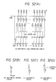
Fig. 82(A) is a flow chart showing the entirety
of a coded dividing processing explained in Figs. 54
to 74, and Fig. 82(B) is a flow chart showing a pre-processing
of the same;
Fig. 83(A) is a flow chart showing the detail of
the division 1 of Fig. 82, and Fig. 83(B) is a flow
chart showing the processing of a division step;
Fig. 84(A) is a flow chart showing the detail of
the entirety of the post-processing of Fig. 82, and
Fig. 84(B) is a flow chart showing the processing of a
quotient correction;
Fig. 85(A) is a flow chart showing the detail of
first remainder correcting means of the post-processing
of Fig. 84, and Fig. 85(B) is a flow chart showing
the processing of second remainder processing means;
Fig. 86 is a diagram for explaining one example
of an instruction description for a coded division of
8 bits ÷ 8 bits;
Fig. 87 is a diagram for explaining one example
of an instruction description for a coded division of
64 bits ÷ 32 bits;
Fig. 88 is a diagram for explaining one example
of an instruction description for a coded division of
32 bits ÷ 32 bits;
Fig. 89 is a diagram for explaining one example
of an instruction description for a coded division of
16 bits ÷ 16 bits;
Fig. 90 is a diagram for explaining one example
of an instruction description for a coded division of
16 bits ÷ 8 bits; and
Fig. 91 is a diagram for explaining one example
of an instruction description for a coded division of
32 bits ÷ 16 bits.
DESCRIPTION OF THE PREFERRED EMBODIMENTS
The present invention will be described in the
following in connection with the embodiments thereof
in the order of items which are broadly itemized into:
a microcomputer adopting an instruction forma of fixed
length having a smaller bit number than that of the
maximum data word length; and coded divisions to be
executed by such microcomputer. The contents of the
former will be described under Items [1] to [17]
whereas the contents of the latter will be described
under Items [18] to [24].
[1] Application System of Microcomputer
Fig. 1 shows one example of a system which makes
use of a microcomputer MCU according to one embodiment
of the present invention. This microcomputer MCU is
coupled through an external control bus ECB, an external
data bus EDB and an external address bus EAB to an
external memory EMRY and an external input/output
block EI/O defined by the user and is further connected
with a port input/output bus PIOB to an external
equipment EEQ. This external equipment EEQ is a
predetermined device to package the microcomputer system.
[2] Block Structure of Microcomputer
Fig. 2 shows the microcomputer MCU according to
one embodiment of the present invention. The microcomputer
MCU, as shown, is packaged in a single semiconductor
substrate such as a silicon substrate by the
well-known semiconductor integrated circuit manufacture
technology. Reference letters CPU appearing in
the Figure designates a central processing unit for
controlling the microcomputer MCU in its entirety.
Letters Port/I/O designate an input/output port to be
used for the central processing unit CPU to input/output
a signal, to drive an external display device and
to inspect the state of an external switch. The central
processing unit CPU inputs/outputs by reading/
writing a register assigned to a certain address.
Letters Port/Cont designate a port for an input/output
of the data bus. Letters Port/Address designate a
port for an input/output of the address bus. Letters
I/O designate such a peripheral device on the chip of
the microcomputer MCU as includes a serial communication
interface, a timer and so on. Letters DMAC designate
a direct memory access (DMA) controller. A ROM
(Read Only Memory) is an instruction memory packaged
on-chip and stores the instructions (i.e., operation
programs) of the central processing unit CPU and a
constant table. A RAM (Random Access Memory) is a
memory packaged on-chip and is used as the working
area of the central processing unit CPU or a primary
storage area for data. Letters BSC designate a bus
state controller for controlling the bus access to the
inside and outside of the microcomputer MCU. Letters
CACHE designate a cache memory, i.e., a storage device
for latching an instruction, which is anticipated to
be most frequently used by recognizing the access pattern
of an instruction of the central processing unit
CPU, to reduce the frequency for accessing to an application
program or the like from an external memory
having a low access rate, thereby to accelerate the
processing. Letters BURST/REFRESH designate a burst/
refresh device for burst control of a continuous data
transfer and for refresh control of a dynamic random
access memory (DRAM) and is applied to a high-speed
page mode access, when the DRAM is used as an external
memory, and to a refreshing of the DRAM. Letters edb
designate an internal data bus coupled through a port
Port/Data to the external data EDB, and letters eab
designate an internal address bus coupled through a
port Port/Add to the external address bus EAB. These
two internal buses are not coupled to the central
processing unit CPU. On the other hand, characters
IDB31-0 designate internal data buses of 32 bits, and
IAB23-0 designate internal address buses of 24 bits.
These two internal buses are coupled to the central
processing unit CPU.
This central processing unit CPU is given an instruction
from the instruction memory ROM or the cache
memory CACHE so that the data issued from the data
memory RAM or the external memory EMRY are subjected
to a predetermined processing in accordance with the
given instruction.
[3] Pin Arrangement of Package of Microcomputer
Fig. 3 conceptionally shows a pin arrangement of
the package of the aforementioned microcomputer MCU.
In the same Figure, free running timers FRT0 and FRT1,
an analog/digital converter A/D, a digital/analog converter
D/A, and serial communication interfaces SCI0
and SCI1 exemplify the peripheral circuit I/O of Fig.
2, and corresponding ports PORT1 to PORT4 shown in
Fig. 3 are input/output ports corresponding to individual
peripheral devices and accordingly to the
port Port/I/O of Fig. 2. The microcomputer MCU is
filled in a QFP type package of 112 pins. Address
buses (A0-23) of 24 bits are connected with the aforementioned
address bus EAB, and data buses (D0-31) of
32 bits are connected with the aforementioned data bus
EDB. These buses A0-23 and D0-31 are used when the
central processing unit CPU, the direct memory access
controller DMAC or the burst/refresh control block
BURST/REFRESH accesses the external memory EMRY.
Clock signals are those for specifying the basic
timing of the instant when the inside of the microcomputer
MCU and its external systems operate synchronously.
If a not-shown quartz oscillator is coupled
to terminals EXTAL and XTAL, for example, it resonates
to oscillate with an electric circuit in the chip of
the microcomputer MCU. This chip detects the oscillating
voltage to generate internally synchronizing
clocks 1 and 2, as will be described hereinafter.
These clocks 1 and 2 are non-overlap clock signals
which have neither of their high periods overlapped,
although not especially limitative thereto. At the
same time, the microcomputer MCU outputs a clock signal
having a waveform and a phase substantially identical
to those of the signal 1 from its terminal CLK
so as to synchronize its external system and the inside
of the LSI. The control signal includes: an
operation mode setting signal and an interruption inputting
signal such as a reset signal (RES) or a
standby signal (STBY); a data bus control signal such
as a read strobe (RD) or a write strobe (WRHH); or a
DRAM refresh control or bus arbitration signal. Letters
Vss and Vcc designate a ground terminal and a
power supply terminal. The port PORT1 inputs/outputs
two channels of the control signal DMAC concerning the
direct memory access controller DMAC. The port PORT2
inputs/outputs the FRT signal for controlling and
reading the free running timers FRT0 and FRT1 from the
outside of the microcomputer MCU. The port PORT3
inputs/outputs the analog signals which are fed to the
analog/digital converter A/D and the digital/analog
converter D/A. Reference potentials of the analog/
digital converter A/D and the digital/analog converter
D/A are fed from terminals AVcc and AVss. The port
PORT4 inputs/outputs the serial communication signals
which belong to three clock, data transmission and
data reception systems for two channels.
[4] Instruction Word Length and Data Word Length
Fig. 4 shows one example of the relation of the
data word length and the instruction word length to a
bus width (i.e., the number of signal lines composing
a bus) in the microcomputer MCU of the present embodiment.
This microcomputer MCU has an architecture of
RISC type and an instruction forma of fixed length.
The buses such as internal data buses IDB31-0, through
which data and instructions are transferred, are given
32 bits (corresponding to 32 signal lines). At this
time, the bit number of later-described various registers
is 32 bits. The data on a memory are arranged at
the units of byte (of 8 bits), word (of 16 bits) and
long word (of 32 bits) in a memory area having a width
of 32 bits. Addresses are assigned at the byte unit
to the memory. As a result: the byte data are accessed
at the unit of n addresses (n: an integer); the
word data are accessed at the unit of 2n addresses;
and the long word data are accessed at the unit of 4n
addresses. Other memory accesses are deemed to belong
to an address error. On the other hand, instructions
are formatted into an instruction format having a
fixed length of 16 bits (corresponding to 16 signal
lines). In short, an instruction of fixed length is
composed of bits of the n-th power of 2, and the relation
of m ≧ n holds, if the number of signal lines
composing the bus width is the m-th power of 2.
In Fig. 4 showing several examples of the aforementioned
instruction format of fixed length of 16
bits: four bits of "rrrr" designate an assigned field
of a source register; four bits of "RRRR" designate an
assigned field of a destination register; bits of
"d---dd" designate a displacement; and bits "ii-i"
designate an immediate data. In an instruction format
of 16 bits, the destination register assigned field
RRRR falls at the eighth bit from the fourth bit with
reference to the lefthand side of the format, and the
source register assigned field rrrr falls at the
twelfth bit from the ninth bit. The lefthand four
bits of the instruction format are assigned to at
least an operation code assigned field. The instruction
system of the microcomputer MCU allows the destination
register assigned field RRRR to be used as a
portion of the operation code assigned field and the
source register assigned field rrrr to be used as a
portion of the displacement or immediate data.
Thanks to adoption of the instruction format of
fixed length of 16 bits for the data word length of 32
bits, where the instruction boundary resides can be
decided before the end of a preceding instruction like
the RISC machine of the prior art having the instruction
format of fixed length of 32 bits, thereby to
warrant the advantage such as simplification of the
instruction decoding process. In addition, the program
capacity can be made smaller than that of the
case in which the instruction format of fixed length
of 32 bits is adopted. In the RISC architecture intended
to accelerate the execution of instructions by
reducing the number of kinds of instructions, there is
a tendency that undefined operation codes increase in
an instruction set. If the instruction length is reduced
at this time to one half of the prior art, the
efficiency of using the program memory can be improved.
Thanks to the reduced instruction word length,
as compared with the data word length, the substantially
useless bit array can be made less than
that of the case, in which the two word lengths are
equalized, so that the efficiency of using the program
memory can be enhanced. As a result, the efficiency
of using the memory for storing the program can be improved
to keep an application field, which uses a
memory having a limited capacity on the board or a
program memory packaged on-chip in the processor, away
from problems such as shortage in the storage capacity
of the program memory at the time of constructing the
system or unavoidably large scale of the memory.
Thus, the system cost can be reduced.
Since, moreover, the instruction format of fixed
length of 16 bits has one half of the data word length
and bus width of 32 bits, an instruction misalignment
to the program memory such that an instruction of single
format is arranged across the boundary of the
memory (or word) occurs less frequently than the case,
in which the instruction word length is shortened by
setting the instruction word length to a fragmentary
bit number (e.g., bit number other than a power of 2)
with respect to the bus width or data word length.
[5] Instruction Control System of CPU
Fig. 5 shows one example of the internal block,
i.e., its instruction control system of the aforementioned
central processing unit CPU. Letters IRH and
IRL designate individual instruction buffers (i.e.,
instruction queues) of 16 bits for latching instructions
of fixed length of 16 bits one by one. These
registers IRH and IRL are individually loaded with the
instructions in one instruction fetch cycle. This is
because the instructions are transferred at the unit
of 32 bits through the internal data buses IDB31-0.
These instructions are loaded in the instruction
register IR1 through a multiplexer MPX. The instruction
register IR1 has 16 bits. This instruction register
IR1 latches the instruction which is present at
the instruction decode stage. In the instruction
register IR1, with reference to the lefthand end indicated
as "RRRR" in accordance with the instruction
format of fixed length of 16 bits, the fifth to eighth
bits are caused to belong to the destination register
field, and the ninth to twelfth bits indicated as
"rrrr" are caused to belong to the source register
field. These fields are fixed in the instruction
field. At this time, as has been described hereinbefore,
the source register field never fails to be
used for selecting the source operand, and the destination
register field never fails to be used for
selecting the second source operand or destination
operand. Each register field may mean a portion of
the operation code or the number of a register. Whether
or not the contents of the register assigned
fields RRRR and rrrr are pieces of information for
selecting a register is determined at the left end of
the aforementioned instruction format of fixed length
by the contents of the 1st to 4th bit operations
codes. Nevertheless, the values of the register
fields RRRR and rrrr are inputted to and decoded by a
source register decoder SRD and a destination register
decoder DRD through the instruction register IR2.
The decoded results by the aforementioned source
register decoder SRD and destination register decoder
DRD are used to decide what of general purpose registers
ROH and ROL, - - -, and R15H and R15L contained
in an execution unit for arithmetic operations is to
be selected. On the other hand, the values of the
register fields RRRR and rrrr outputted from the a-forementioned
instruction register IR2 are fed through
temporary latches WBR0 and WBR1 to a write back register
decoder WBRD so that the arithmetic results obtained
by the instruction executions are written for
selecting the general purpose registers in accordance
with the decoded results. Moreover, the values of the
register fields RRRR and rrrr, i.e., the register numbers
latched in the aforementioned temporary latch
WBR1 and being used are fed to a register content
check block RCCB so that they are compared with the
outputs of the instruction registers IR1 and IR2 to
find out an even (or register conflict), in which each
instruction, e.g., a subsequent instruction accesses a
common register when the instructions sequentially
fetched are executed in the pipe-line manner. The
register conflict is fed to a flag operation & pipe
control decoder FO&PCD in response to the signal S1.
If the signal S1 thus asserted is fed to the flag
operation & pipe control decoder FO&PCD, skip controls
are executed in accordance with the number of instruction
execution cycles being done, to cancel or delay
the execution cycles of the instructions using the
conflicting registers. In short, when the flag operation
& pipe control decoder F0&PCD outputs the control
signal Skip, the decoding of the instruction to be
subsequently executed is delayed in the source register
decoder SRD and the destination register decoder
DRD. As a result, the execution cycle of a succeeding
instruction is started at a timing after the writing
of the conflicting registers is ended by executing the
preceding instruction.
The instruction latched by the aforementioned instruction
register IR1 is fed to a mapping control
block MCB to index the addresses of a high-speed control
read only memory (i.e., Hardware Sequence ROM)
HSC-ROM. This mapping control block MCB has a role to
calculate the entry address of a proper high-speed
control read only memory MHSC-ROM in accordance with
the content. The high-speed control read only memory
HSC-ROM has its output composed of two portions: a
micro code field MCF and a pipe control field PCF,
which are latched by a hardware sequence control instruction
register HIR such as a micro instruction
register. The former in the micro instruction field
feeds a control signal to the execution unit EXEC
through a shallow decode logic, i.e., an instruction
decoder ID. The latter establishes the sequence of an
instruction having two or more cycles through the flag
operation & pipe control decoder FO&PCD or controls
the pipe line. The flag operation & pipe control decoder
FO&PCD has eight flags C, W, B, L, M, I, S and S
for controlling the pipe lines. Moreover, this flag
operation & pipe control decoder FO&PCD has a status
register SR which has a true bit T (as will be shortly
referred to as "T bit") used for condition branching.
This T bit is set to the truth or false of the arithmetic
result of selected conditions described in the
instruction, as will be described hereinafter.
The content of the aforementioned instruction
register IR1 is transferred before an arithmetic execution
phase (EX) to the instruction register IR2 so
that whether or not a conflict is caused between instructions
in the pipe line state of later memory
access phase (MA) and write back phase (WB) is checked
through the aforementioned register content check
block RCCB, and this result is outputted as the signal
S1. What is stored at this time in the instruction
register IR2 is the value of the register field. The
values of the register fields RRRR and rrrr latched in
the instruction registers IR1 and IR2, as has been
described hereinbefore, are fed to the aforementioned
source register decoder SRD, destination register decoder
DRD and write back register decoder WBRD. These
source register decoder SRD, destination register decoder
DRD and write back register decoder WBRD generates
a selection signal for selecting one pair of
the sixteen general purpose registers ROH and ROL, - -
-, and R15H and R15L and feeds it to the execution
unit EXEC.
The memory interface MIF detects whether or not
the central processing unit CPU has to access a memory
and whether the memory is of the read or write type,
and feeds a signal necessary for accessing the memory.
On the other hand, an instruction fetch & instruction
register control block IF&IRC has a function to determine
whether or not an instruction fetch from a memory
is necessary and when the contents of the instruction
registers IRH and IRL are to be updated, and to output
a necessary signal. The function of this instruction
fetch & instruction register control block IF&IRC is
to output a predetermined control signal with reference
to the state of the pipe line, the state of the
memory and the state of the instruction queues (IRH
and IRL) thereby to control the instruction queue or
the instruction fetch. What features the present embodiment
is that the instruction fetch is carried out
at the unit of 32 bits so that it contains two instructions
having an instruction length of 16 bits.
This makes it unnecessary to fetch again the instruction,
which has been fetched simultaneously as the
preceding instruction is fetched, in another phase.
These events are totally judged to control when the
instruction fetch is to be executed. The instruction
fetch & instruction register control block IF&IRC is
constructed as an finite state machine, and a detailed
description of the structure of this machine will be
omitted because the structure per se is well known in
the art.
Incidentally, letters IMB appearing in Fig. 5
designate a buffer for sending immediate data contained
in an instruction to the execution unit EXEC.
Moreover, the instruction queues IRH and IRL and the
latch timing of the instruction register IR1 are synchronized
with the aforementioned clock signal 1.
The latch timings of the instruction register IR2, the
micro instruction register MIR and the registers WBR0
and WBR1 and the output timing of the signal S1 by the
aforementioned register content check block RCCB are
synchronized with the aforementioned clock signal 2.
Since the data bus width is 32 bits whereas the
fixed length instruction is 16 bits, there are provided
two instruction buffers IRH and IRL. Despite of
this provision, however, the number of instruction
buffers is determined depending upon how many fixed
length instructions can be transferred within the data
bus width, for example: four instruction buffers in
case of a fixed length instruction of 8 bits; and
eight instruction buffers in case of a fixed length
instruction of 4 bits.
[6] Execution Unit of CPU
Figs. 6 and 7 show one example of the execution
unit EXEC of the central processing unit CPU. In the
two Figures, buses indicated at A, B, C and D are commonly
connected. The execution unit EXEC includes: an
instruction fetch block IFB and a general purpose
block GRB for fetching an instruction and updating a
program counter; an operation block OPB for addition/
subtraction and shift operations; and memory access
block MAB and a multiplication block MULT for accessing
a memory and aligning data. These individual
blocks are coupled to one another through the four
data buses A, B, C and D having a width of 32 bits.
The aforementioned instruction buffers (or instruction
queues) IRH and IRL, multiplexer MPX and instruction
register IR1 forming part of the aforementioned
instruction fetch block IFB are shown in the
block structure of Fig. 5 separately of the execution
unit EXEC but may be contained in the execution unit
EXEC, as shown in Fig. 6. An immediate buffer IMB is
a logic for cutting and bit-shift, if necessary, immediate
data. Letters PCH and PCL designate program
counters for latching addresses for fetching an instruction.
An arithmetic unit high AUH and an arithmetic
unit low AUL are adders capable of performing an
addition of 32 bits for updating the program counters.
A procedure address register high PRH and a procedure
address register low PRL are procedure address registers
for latching return addresses for a function
call. A vector base register high VBRH and a vector
base register low VBRL are used as storage areas of an
interrupt vector area for latching the base addresses.
A global base register high GBRH and a global base
register low GBRL are used as storage registers for
the base address of the I/O. A break register high
BRH and a break register low BRL are used as storage
registers for return destination addresses from the
break routine.
The aforementioned general purpose register block
GRB includes sixteen general purpose registers of 32
bit length, as indicated at ROH and ROL to R15H and
R15L. In the aforementioned operation block OPB, a
shifter high SFTH and a shifter low SFTL are hardware
for bit shifts and rotations. An arithmetic logic
unit high and an arithmetic logic unit low are operators
for arithmetic logical operations. Letters
SWP&EXT designate a hardware for executing a swap instruction,
a code (or sign) extension or a zero extension.
An aligner ALN is a hardware for aligning the
data which are accessed in byte or word from a memory
or I/O. A memory read buffer high MRBH and a memory
read buffer low MRBL are temporary registers for
latching the data which are read from a memory. A
memory write buffer high MWBH and a memory write
buffer low MWBL are temporary registers for latching
data to be written in a memory. A memory address
buffer high MABH and a memory address buffer low MABL
are temporary registers for latching addresses at the
time of a memory access. A MULT buffer MLTB is a temporary
register for transferring a multiplier and a
multiplicant to the multiplication block MULT.
The connection relations of the inside and outside
of the central processing unit CPU through the
buses are as follows. Specifically, letters MTBL and
MTBH are bilateral special purpose buses for connecting
the multiplication block MULT. In Figs. 6 and 7,
letters IDBH and IDBL correspond to the data buses
IDB31-0 of Fig. 2, and letters IABH and IABL correspond
to the address buses IAB23-0 of Fig. 2. The
values of the aforementioned program counters PCH and
PCL are outputted to the address buses IABH and IABL,
and the instruction buffers IRH and IRL fetch the data
from the data buses IDBH and IDBL so that the outputs
of the temporary registers MWBH and MWBL are fed to
the data buses IDBH and IDBL. The temporary registers
MRBH and MRBL input the data from the data buses IDBH
and IDBL and the special purpose buses MTBH and MTBL.
The address informations latched by the temporary
registers MABH and MABL are outputted to address buses
IABH and IABL. The multiplying temporary register
MLTB has its output fed to the special purpose buses
MTBH and MTBL.
[7] Pipe Line Stage by CPU
Fig. 8 shows one example of a stage of a pipe
line processing by the central processing unit CPU.
This central processing unit CPU has a basic pipe line
structure of five stages having the following basic
phases:
In Fig. 8 showing one example of the execution content
of each pipe stage, the Address Bus correspond to the
address buses IAB23-0 of Fig. 2, and the Data Bus correspond
to the IDB31-0 of the same. Letters IR of
Fig. 8 correspond to the instruction buffers IRH and
IRL of Figs. 6 and 5. In Fig. 8, letters A-Bus, B-Bus,
C-Bus and D-Bus are the A bus, B bus, C bus and D
bus of Fig. 7, respectively. Likewise, letters MAB
and MRB of Fig. 8 are the MABH, MABL, MRBH and MRBL of
Fig. 7.
[8] Pipe Line Sequence in Register Conflicting
State
The pipe line sequence in the aforementioned register
conflicting state will be described with reference
to Fig. 9. First of all, the meanings of signals
shown in the same Figure will be described in the following.
The waveforms of the aforementioned non-overlap
two-phase clock signals 1 and 2 acting as
operation reference clock signals are shown at the top
of Fig. 9. One cycle is defined as a period starting
from the rise of the clock signal 1 and ending the
next rise of the signal 1. Subsequently, the states
of an address bus and a data bus are shown. Next letters
IRLatch designate a latch signal of an instruction
buffer (IR(32 bits) or IRH and IRL). The IRLatch
presents an input latch signal waveform of the IR1
register. The IR1 (16 bits) latches the instruction
which is present at an instruction decode stage. The
aforementioned hardware sequence control instruction
register HIR is a register for latching a partially
decoded micro code, a sequence information or a pipe
line control information. Letters Reg. Content Flag
appearing in Fig. 9 designate a flag indicating it
necessary to check the conflict between an LOAD instruction
and an instruction using the execution unit
EXEC. This conflict is checked in a 4th cycle to set
a Content Flag (or C flag). At the same time, there
is set a LOAD Flag (or L flag) indicating it necessary
to load an operand. Likewise, there is set in the 4th
cycle a Bus Cycle Flag (or B flag) indicating a bus
operation necessary. This flag indicates whether or
not the bus cycle is being executed. An instruction
fetch inhibit flag (i.e., IF Inhibit Flag: I Flag) is
one indicating that an instruction fetch is interrupted
and replaced by a data access. A skip signal
(i.e., Skip Sig.) is a flag meaning that a processing
to be executed in the execution unit EXEC in that
cycle is canceled. The Execution indicates a processing
to be executed in the execution unit EXEC. The
Reg. Write is a signal to be written in a register.
In response to the Reg. Write in the ordinary operation,
the destination register, as instructed, latches
through the C-Bus. At the time of executing the LOAD
instruction and the MULT instruction, the destination
register, as instructed, latches through the D-Bus.
In this meaning, the signal Reg. Write is shown as
divided those for the C-Bus and the D-Bus in the timing
chart so that the writing operation is executed in
preference of the C-Bus if the two signals Reg. Write
for the C-Bus and D-Bus conflict in the same register.
In short, only the write from the C-Bus is executed.
The signal written in the 5th cycle, as indicated dotted
lines, indicates the write in the register which
is inhibited by the Skip Sig. The MAB means a memory
address bus for outputting an address when a data access
is executed. The MRB Latch meaning a memory read
buffer is a signal for latching data. The PC indicates
the value of a program counter.
Fig. 9 is a timing chart exemplifying the sequences
between LOAD instructions (LOAD @R1, R2) and ADD
instructions (ADD R2, R3). The register R2 for the
LOAD instruction to latch the data and the register R2
for the ADD instruction to use are so common that the
value of the register R2 is used for the operations
between its value determined if the instruction execution
is performed in the ordinary pipe line flow. In
this example, what timing the pipe line control is to
be executed at is shown over seven cycles when the
uses of the registers R2 conflict. The lowermost
column indicates the situations of execution of the
pipe line. Since the register R2 of the destination
of the LOAD instruction and the source register R2 of
the ADD instruction conflict, a stall (or delay) occurs
at the 5th cycle, as shadowed. For this stall,
it becomes necessary at first to detect whether or not
the register conflicting state takes place and to
recognize how many cycle the execution cycle (EX) is
to be delayed for avoiding the register conflict. The
former detection is carried by asserting the signal S1
outputted by the aforementioned register content check
block RCCB for comparing the register selecting information
contained in the preceding instruction outputted
by the aforementioned register WBR1 and the
register selecting information (e.g., the information
contained in the ADD instruction for selecting the
register R2 according to this example) contained in
the succeeding instruction. The latter recognition
can be achieved from the decoded result of the operation
code. Since the number of the execution cycle
(EX) of the LOAD instruction is one in the shown example,
the stall occurs only in the 5th cycle.
Fig. 10 shows another example of the pipe line
sequence in the register conflicting state. Fig. 10
is a timing chart exemplifying the sequences among the
MULT instructions (MUL R1, R2) as multiplying instructions,
the ADD instructions (ADD R4, R3) and the SUB
instructions (SUB R3, R2). The register R2 for the
MUL instruction to latch the data and the register R2
to be used by the SUB instructions are common. Unless
the register conflicting state is reflected upon
the pipe line sequences, it occurs that the register
R2 is used for another operation before its value is
determined if the instruction is executed. In the
present example, what timing the control of the pipe
line is executed at in case of such conflict of register
uses is shown over seven cycles. The format of
expression of the present Figure is similar to that of
Fig. 9 and illustrates the executions of multiplications
in four cycles, although not detailed. The MULT
instructions are executed in four stages EX, ML, ML
and ML. The multiplier can execute the multiplications
for latching the result of 16b*16bin 32b in the
four cycles. These calculations can be executed by
determining the partial product of 16b*4b and their
cumulative sum for each cycle. In case of this example,
the SUB instruction is fetched in the register
R1 with a delay of 2 cycles from the MULT instruction,
and the execution cycle (EX) of the SUB instruction is
delayed by two cycles because the MULT instruction are
multiplied in the four cycles EX, ML, ML and ML.
[9] Pipe Line Sequence at Memory Access
Conflicting Time
Fig. 11 shows a pipe control sequence exemplifying
the case, in which a data fetch from a memory and
an instruction fetch conflict. In this case, the data
fetch is preferred so that the instruction execution
schedule containing a conflicting instruction fetch is
shifted in its entirety. For this control, the instruction
fetch wait flag (IF Wait Flag) is set to
delay the start of the instruction fetch cycle while
the load flag (LOAD Flag) and the bus cycle flag (Bus
Cycle Flag) are conflicting.
[10] Sequence of Instruction Execution of Plural
Cycles
Fig. 12 is a timing chart showing one example
when a plurality of cycle instructions are executed.
Here will be explained by way of example an instruction
"AND.B #imm, @R1" or a kind of AND instructions
(i.e., logical product). This is an instruction for
calculating the logical product between the 8 bit data
of a memory selected relative to the register R1 and
the 8 bit immediate data. This AND.B instruction is a
plurality cycle instructions to be executed in response
to the macro instruction 1, the micro instruction
1 and the micro instruction 2. The aforementioned
macro instruction 1 is an instruction for
fetching a byte operand from the area of a memory,
which is selected according to the content of the
register R1. The aforementioned micro instruction 1
is an instruction for taking an AND of the aforementioned
byte operand and the immediate data. The
aforementioned micro instruction 2 is an instruction
for writing the byte operand in the area of a memory,
which is selected according to the content of the
register R1.
The execution content of the aforementioned AND.B
instruction is described in the C language:
With reference to this description, there are idle
cycles between the ID (Instruction Decode) stage and
the EX (Execution) stage of the
micro instruction 1
and between the µ-IF (Micro Instruction Fetch) stage
and the ID stage of the
micro instruction 2. This is
because the operand fetched at the MA (Memory Access)
stage of the
macro instruction 1 has to be used at the
EX (Execution) stage of the
micro instruction 1.
The instructions to be assigned to the central
processing unit CPU are: data transfer instructions
shown in Figs. 13 and 14; logical operation instructions
shown in Fig. 15; arithmetic operation instructions
shown in Figs. 16 and 17; shift instructions
shown in Fig. 18; branch instructions shown in Fig.
19; and system control instructions shown in Figs. 20
and 21. Fig. 22 explains the description formats of
Figs. 13 to 21. According to these formats, the items
of the instructions in Figs. 13 to 21 are mnemonically
indicated. The addressing modes in this mnemonic indications
are tabulated in Fig. 23. As apparent from
the various instruction codes, all of the integer calculations,
branching methods and control instructions
of the general purpose register system can be selected
even in the 65,536 combinations which can be expressed
in the instruction format of fixed length of 16 bits.
The decoding can be realized with less logical expressions
by devising the bit assignments to group instructions
of similar functions. An instruction array
having the operation code starting from "1111" is
wholly reserved so that calculations of single or
double accuracy can be selected in conformity with the
IEEE floating point standards.
[12] Displacement Length of Branch Instruction
Figs. 24, 25, 26 and 27 plot the relations between
the displacement lengths of branch instructions
and instructions in various programs extracted as
samples and the appearance frequencies of the instructions
having those displacement lengths. Figs. 24 and
25 relate to conditional branch instructions (i.e.,
branch instructions) and unconditional branch instructions
(i.e., branch always instructions); Fig. 26 relates
to subroutine call instructions; and Fig. 27 relates
to jump instructions or jump subroutine instructions.
Here, the "branch" is to select one of numerous
instruction sets which can be selected in the execution
of a computer program. The "jump" means a
departure from the implicit or specific execution order
of instructions, which is actually done in the execution
of the computer program. The "displacement"
is used to select a jumped address. For the more bit
number of the displacement length, therefore, the farther
address can be jumped to.
The frequency distributions of the displacement
in response to the branch instructions, as shown in
Figs. 24 to 26, are the data which were obtained by
analyzing the various programs of Microcomputer H8/500
of Hitachi, Ltd. These Figures illustrate the distributions
of the displacement values of the individual
kinds of the branch instructions used. The abscissa
indicates the log 2 values of the used displacement
values. At the righthand of the origin 0,
the log 2 {i.e., displacement} is expressed by a positive
integer (1, 3, 5, 7, - - -) in case the displacement
value is positive. At the lefthand, the -log 2
{i.e. -displacement} is expressed by a negative number
for a displacement having a negative value. The
ordinate indicates the appearance frequency at the
unit of %. The data were sampled for nine different
programs.
As could be apparent from Figs. 24 and 25, the
branch instructions and the branch always instructions
having the higher appearance frequencies are distributed
the closer to the center so that the distribution
can be substantially covered with a displacement
of 8 bits. It could also be found that the
distribution of the subroutine call instructions of
Fig. 26 can be wholly covered with a displacement
field of 12 to 13 bits although it is considerably
wide. In case of the jump instructions or jump subroutine
instructions shown in Fig. 27, moreover, the
value of the abscissa takes such a displacement as is
defined to mean the difference between the address, at
which the jump instruction is present, and the address
of the jump destination. It could be found that the
jump destination is also far.
In the microcomputer MCU of the present embodiment,
the displacement of the conditional branch instructions
is fixed at 8 bits, and the displacement of
the subroutine branch instructions and the unconditional
branch instructions is fixed at 12 bits so that
those instructions are confined in the instruction
format of fixed length of 16 bits. In the various
branch instructions shown in Fig. 19, for example: the
individual instructions BC, BT and BF are made to
belong to the conditional branch instructions; the instruction
BSR in the same Figure is made to belong to
the subroutine branch instructions; and the instruction
BRA is made to belong to the unconditional branch
instructions. The detailed contents of the individual
instructions should be referred to the description
items of instructions, as follows.
In the modular programming method for preparing a
program as a set of relatively small subroutines (or
functions), the conditional branch instructions will
jump within the functions. Since most functions have
a size as large as several hundreds bytes, the distribution
can be substantially covered with the displacement
of 8 bits. On the other hand, the subroutine
branch has a tendency to jump to the outside
of a function itself, i.e., to a far place so that it
requires a displacement of a larger bit number than
that of the condition branch instruction. The unconditional
branch may be used for calling another function
at the last of functions so as to accelerate the
program. Since it seems advantageous that the unconditional
branch be handled similarly to the subroutine
branch condition, the bit number of the displacement
is equalized to that of the subroutine branch. Thus,
the fixed assignment of the proper displacement length
according to the kind of the branch instruction contributes
to realization of the instruction format of
fixed length of 16 bits without any substantial trouble.
[13] Processing of Immediate Data
In case the instruction format of 16 bit fixed
length is adopted, it is not practical to limit all
the immediate values to 16 bits or less in view of the
fact that the data word length is 32 bits. In the
present embodiment, a method of using the value of a
register such as the program counter PC and the relative
address is adopted so as to select the immediate
values of 16 bits or more within one instruction format.
The instructions for the immediate processing are
exemplified by the load instructions shown in Fig. 13,
such as MOV.W@(disp, PC)Rn or MOV.L@(disp, PC)Rn.
These instructions are those for storing the immediate
data in the general purpose register Rn. If the data
are words/long words, there are referred to the data
in a table stored in the address which is specified by
adding the displacement to the program counter PC. If
the data are words, the displacement is shifted leftward
by 1 bit to 9 bits so that the relative distance
from the table is changed from -256 to +254 bytes.
The program counter PC is the head address which is
behind the present instruction by two instructions.
This makes it necessary to arrange the word data at
the boundary of 2 bytes. If the data are the long
words, the displacement is shifted leftward by 2 bits
to 10 bits so that the relative distance from the
operand is changed from -512 to +508 bytes. The program
counter PC is the head address which is behind
the present instruction by two instructions, but its
less significant 2 bits are corrected to B and 00.
This makes it necessary to arrange the long word data
at the boundary of 4 bytes.
[14] Implicit Register Selection
The implicit register selection is said to select
a general purpose register fixed as an operand notwithstanding
that no register selecting field is present
in an instruction. The general purpose register,
as specified herein, is used for determining a memory
address, for example, or for storing the data fetched
from a memory. The instruction for this implicit register
selection can be exemplified by the MOV @(disp.
R1)R0 or MOV R0, @(disp, R1), as shown in Fig. 14. As
is apparent from the codes corresponding to the instruction
in the same Figure, the instruction contains
only the operation code and the displacement dddddddd
of 8 bits but not the register selecting field. This
displacement is used for determining a memory address
together with the value of the implicitly selected
register R1. Thanks to this implicit register selection,
even in an instruction requiring the value of
the register and the displacement, the instruction
word length can be restricted within 16 bits without
any reduction in the bit number required as the displacement.
[15] Functionally Composite Instruction
The functionally composite instruction can be exemplified
by a bit operation instruction such as AND.B
#imm, @R1 shown in Fig. 15. This instruction is one
composed of three instructions for taking a logical
product (i.e., AND operation) between the 8 bit data
of a memory selected relative to the register R1 selected
implicitly like before and the immediate data
of 8 bits to execute the reading of the memory, the
AND operation and the write return of the result of
the AND operation in said memory. The operation of
this kind appears highly frequently in controlling the
packaged devices, and the adoption of such functionally
composite instruction in the instruction format of
16 bit fixed length contributes to an improvement in
the code efficienty.
[16] Truth/False Setting Instruction for Selected
Condition
An instruction for setting the truth/false of the
arithmetic result for a selected condition can be exemplified
by eight kinds of CMP instructions shown in
Fig. 16, for example. These are instructions for comparing
operands to set the comparison result to the T
(True) bit of the aforementioned status register SR.
For example, the instructions as designated at COMP/
EQ, Rm and RnFF compare whether or not the values of
the registers Rm and Rn are equal, and set the T bit
to 1, if YES, but clear the same to 0. By assigning
the T bit to the status register so that the operation
of setting the truth/false for the compared result to
the T bit may be executed in response to one instruction
of the instruction format of 16 bit fixed length,
the next instruction such as the aforementioned conditional
branch instruction BT for the operation based
on the resultant truth/false may refer directly to the
T bit. Thus, the description of the condition necessary
for the arithmetic result according to the preceding
instruction need not be made in said BT instruction
itself so that the area of the displacement
necessary for the BT instruction can be accordingly
enlarged in the limited instruction format of fixed
length. As a result, this structure contributes to
realization of the instruction format of 16 bit fixed
length.
[17] List of Instructions
The featuring ones of the instructions of having
the formats of 16 bit fixed length have been representatively
described hereinbefore. In order to clarify
the whole aspect of the instruction format of 16
bit fixed length, all the instructions of the microcomputer
of the present embodiment will be further
described sequentially in the alphabetical order. The
descriptions of the individual instructions include
the names of instructions, the formats (wherein "imm"
and "disp" designate numerical values or symbols)
expressed by the input formats of the assembler, the
notes for using the instructions, the descriptions of
the operations expressed by the C language, the operation
examples (indicating the states before and after
the instruction executions) exemplified assemblermnemonically,
and the codes. Before the descriptions
of the individual instructions, here will be described
the register structures as the programmer's models to
be noted when a program is to be executed, with reference
to Fig. 28. The registers as the programmer's
models are exemplified not only by the aforementioned
general purpose registers R0 (i.e., ROH, ROL) to R15
(i.e., R15H, R15L) but also by control registers such
as a status register SR, a procedure register PR
(i.e., PRH, PRL), a global base register GBR (BGRH,
GBRL), a program counter PC (PCH, PCL), a vector base
register VBR (VBRH, VBRL) or a break register BR (BRH,
BRL). In the example of Fig. 28: the register R0 is
an accumulator; the register R1 is an index register;
and the register R15 is a stack pointer. In the status
register SR of Fig. 28: the M/Q bit is referred to
in the DIV instruction; the I bit is a mask bit; the
sign "-" is a reserved bit; the D bit is referred to
in the PASS instruction; the C bit is one reflecting
on the carry/borrow/overflow/underflow/shift-out; and
the T bit is one expressing the truth (1) and the
false (0), as has been described hereinbefore.
The descriptions of the operations, whose contents
are indicated in C, assume the use of the following
resources, although not especially limitative
thereto:
The data Data are written with their individual
sizes in the address Addr.
The writes of the words other than the address
(2n) and the long words other than the address
(4n) are detected as address errors.
Delay_Slot (unsigned long Addr);
The slot instruction of the address (Addr-4) is
executed. This means that the execution is
shifted for Delay_Slot(4) to the instruction of
not the 4th address but the 0-th address. If,
moreover, the execution is to be shifted from
that function to the following instructions,
these are detected as the slot invalid instructions
immediately before the execution:
In addition, it is assumed that the PC indicates the
address of 4 bytes (i.e., 2 instructions) before of
the instruction being executed. This means that
(PC=4;) indicates a shift of execution from the instruction
of not the 4th address but the 0th address.
In the example of use described in the assembler
mnemonic format, the codes indicate the binary codes.
In the mnemonic: the following expansions
are made in codes:
| r | rrrr |
| R | RRRR |
| imm | iiiiiiii |
| disp | dddd or |
| | dddddddd or |
| | dddddddddddd. |
The SS in the MOV instruction code is
expanded in the following manner in accordance
with the operand size:
ADD (Addition) Instruction
Format:
Description:
The contents of the general purpose registers Rn
and Rm are added, and the result is stored in the
Rn. The general purpose register Rn and 8 bit
immediate data can be added. The 8 bit immediate
data are code-expanded to 32 bits so that they
are used with subtractions.
Operation:
Example of Use:
Description:
The contents of the general purpose registers Rn
and Rm and the C bit are added, and the result is
stored in the Rn. According to the arithmetic
result, the carry reflects upon the C bit.
Operation:
Example of Use:
Description:
The contents of the general purpose registers Rn
and Rm are added, and the result is stored in the
Rn. Even if an overflow occurs, the result is
limited to a range of H'7FFFFFFF to H'80000000.
At this time, the C bit is set.
Operation:
Example of Use:
Description:
The contents of the general purpose registers Rn
and Rm are added, and the result is stored in the
Rn. If an overflow occurs, the C bit is set.
Operation:
Example of Use:
Description:
The logical product of the general purpose registers
Rn and Rm are added, and the result is
stored in the Rn. A special type can be taken
from either the logical product between the general
purpose register R0 and the zero-expanded
8 bit immediate data or the 8 bit memory relative
to the R1 and the 8 bit immediate data.
Note:
In the AND #imm, R0, the more significant 24 bits
of the R0 are always cleared as a result of the
operation.
Operation:
Example of Use:
Description:
This instruction is a conditional branch one
referring to a T/C bit. For T = 1, the BT is
branched, but the BF executes a next instruction.
For T = 0, on the contrary, the BF is branched,
but the BT executes a next instruction. The BC
is branched for C = 1 but executes a next instruction
for C = 0. The destination of branch
is an address, in which the displacement is added
to the PC. This PC is the leading address of the
instruction which is behind the present instruction
by two instructions. Since the displacement
is shifted leftward by 1 bit to have 9 bits, the
relative distance from the branch destination
ranges from -256 to +254. If the branch destination
fails to be reached, this is coped with by
the combination with the BRA instruction or the
JMP instruction.
Operation:
Example of Use:
Description:
This is an unconditional delay branch instruction.
The branch destination is located at the
address which is the addition of the displacement
to the PC. This PC is the leading address which
is behind the present instruction by two instructions.
Since the displacement is shifted leftward
by 1 bit to 13 bits, its relative distance
from the branch destination ranges from -4096 to
+4094. If the branch destination fails to be
reached, a change has to be made to the JMP instruction.
At this time, the branch destination
address has to be transferred to the register in
response to the MOV instruction.
Note:
Because of the delay branch instruction, the instruction
immediately after the present instruction
is executed prior to the branch. No interruption
is accepted between the present instruction
and the instruction immediately after. This
instruction immediately after is recognized as an
invalid one if it is a branch instruction.
Operation:
Example of Use:
Description:
A break exceptional process is started. Specifically,
after an acknowledge signal is returned to
an external device, the PC is relieved to the BR
to make a branch to a break interrupt routine in
accordance with a predetermined vector. The PC
is the leading address of the present instruction.
The content of the VBR is independent of
the calculation of a vector address. The VBR is
combined with the RTB and is used in a break
routine call.
Note:
The present instruction will not accept an interruption.
The BR is used together with a hardware
break caused by a break terminal. Hence, any
break redemand during the breaking should be
avoided. The PC but not the SR is protected by
the BR. The SR has to be relieved, if necessary,
to a register or memory in response to the STC
instruction.
Operation:
Example of Use:
Description:
This makes a branch to a selected address procedure.
The content of the PC is relieved to the
PR and is branched to the address which is the
addition of the displacement to the PC. This PC
is the leading address which is behind the
present instruction by two instructions. Since
the displacement is shifted leftward by 1 bit to
13 bits, its relative distance from the branch
destination ranges from -4096 to +4094. If the
branch destination fails to be reached, a change
has to be made to the JSR instruction. At this
time, the branch destination address has to be
transferred to the register in response to the
MOV instruction. The JSR instruction is combined
with the RTS and is used for a procedure call.
Note:
Because of the delay branch instruction, the instruction
immediately after the present instruction
is executed prior to the branch. No interruption
is accepted between the present instruction
and the instruction immediately after. This
instruction immediately after is recognized as an
invalid one if it is a branch instruction.
Operation:
Example of Use:
Description:
The C bit of the SR is cleared.
Operation:
Example of Use:
Description:
The T bit of the SR is cleared.
Operation:
Example of Use:
Description:
The general purpose registers Rn and Rm are compared.
If the result reveals that a selected
condition (cond) holds, the T bit of the SR is
set. If NO, the T bit is cleared. The content
of the Rn is unchanged. Eight conditions can be
selected. For the two conditions of the PZ and
the PL, the Rn and 0 are compared.
| Mnemonic | Description |
| CMP/EQ Rm,Rn | T=1 for Rn=Rm |
| CMP/GE Rm,Rn | T=1 for coded values Rn≧ Rm |
| CMP/GT Rm,Rn | T=1 for coded values Rn> Rm |
| CMP/HI Rm,Rn | T=1 for uncoded values Rn> Rm |
| CMP/HS Rm,Rn | T=1 for uncoded values Rn≧ Rm |
| CMP/PL Rn | T=1 for Rn> 0 |
| CMP/PZ Rn | T=1 for Rn≧ 0 |
| CMP/STR Rm,Rn | T=1 if any byte is equal |
The content of 32 bits of the general purpose
register Rn is subjected to one-step division
with the content of the Rm. The DIVOS is an intialization
instruction for a coded division to
store the MSB of the dividend (Rn) in the Q bit,
the MSB of the divisor (Rm) in the M bit, and the
EOR of the M bit and the Q bit in the C bit. The
DIVOU is an initialization instruction for a uncoded
division to clear M/Q/C bits to zero. A
quotient is obtained by repeating the DIV1 (in
combination with the ROTCL, if necessary) by the
number of times of the bit number of the divisor.
In this repetition, an intermediate result is
latched in M/Q/C bits of the assigned register
and the SR. The arithmetic result is not warranted
if the procedures are unnecessarily rewritten
by a software.
The sequence of the division can be referred to
the following examples of use.
The zero division, the detection of the overflow
and the arithmetic of the remainder are not prepared.
Operation:
Example 1 of Use:
Example 2 of Use:
Example 3 of Use:
Example 4 of Use:
Description:
An exclusive OR is taken between the content of
the general purpose register Rn and the Rm, and
the result is latched in the Rn. A special form
can be exemplified by either an exclusive OR between
the general register R0 and the zero-extended
8 bit immediate data or an exclusive OR
between an 8 bit memory and a 8 bit immediate
data relative to the R1.
Operation:
Example of Use:
Description:
The content of the general purpose register Rm is
code-extended, and the result is latched in the
Rn. In case of byte assignment, the content of
the bit 7 of the Rm is copied from the bit 8 to
the bit 31. In case of word assignment, the content
of the bit 15 of the Rm is copied from the
bit 16 to the bit 31.
Operation:
Example of Use:
Description:
The content of the general purpose register Rm is
zero-extended, and the result is latched in the
Rn. In case of byte assignment, the value 0 is
inserted into the bits 8 to 31 of the Rn. In
case of word assignment, the value 0 is inserted
into the bits 16 to 31.
Operation:
Example of Use:
Description:
A delay branch is unconditionally made to an assigned
address. The branch destination is the
address which is expressed with the 32 bit data
of the content of the general purpose register
Rn.
Note:
An instruction immediately after the present instruciton
is executed prior to the branch because
of a delay branch instruction. No interruption
is accepted between the present instruction and
the instruction immediately after. This after
instruction is recognized as an invalid one if it
is a branch instruction.
Operation:
Example of Use:
Description:
A branch is made to a procedure of an assigned
address. The content of the PC is resumed to the
PR, and the content of the general purpose register
Rn is branched to the address which is expressed
with 32 bit data. The PC is a leading
address which is behind the present instruction
by two instructions. The PC is combined with the
RTS and is used for the procedure call.
Note:
An instruction immediately after the present instruciton
is executed prior to the branch because
of a delay branch instruction. No interruption
is accepted between the present instruction and
the instruction immediately after. This after
instruction is recognized as an invalid one if it
is a branch instruction.
Operation:
Example of Use:
Description:
A source operand is latched in the control
register CRn.
Note:
No interruption is accepted by the present
instruction.
Operation:
Example of Use:
Description:
The content of the general purpose register R0
is latched in the control register BR.
Note:
No interruption is accepted by the present
instruction.
Operation:
Example of Use:
Description:
The content of the general purpose register R0
is latched in the control register VBR.
Note:
No interruption is accepted by the present
instruction.
Operation:
Example of Use:
Description:
Immediate data are latched in the general purpose
register Rn. The data are code-expanded to 32
bits. If the data are a word/long word, reference
is made to the data in the table, which are
latched by adding the displacement to the PC. If
the data are a word, the displacement is shifted
leftward by lbit to 9 bits so that the relative
distance from the table is -256 to +254 bytes.
The PC is the leading address which is behind the
present instruction by two instructions. This
makes it necessary to arrange the word data in
the boundary of 2 bytes. If the data are a long
word, the displacement is shifted leftward by 2
bits to 10 bits, the relative distance from the
operand is -512 to +508 bytes. The PC is the
leading address, which is behind the present instruction
by two instructions, and its less significant
two bits are corrected to B, 00. This
makes it necessary to arrange the long word data
in the boundary of 4 bytes.
Note:
The table is not automatically skipped so that it
is interpreted as an instruction without any
countermeasure. In order to avoid this, the
table has to be arranged either at the head of a
module or after the unconditional branch instruction.
If, however, the table is carelessly arranged
immediately after the BSR/JSR/TRAP, a simple
return will conflicts with the table. When
the present instruction is arranged immediately
after the delay branch instruction, the PC is the
leading address +2 of the branch destination.
The table access of the present instruction is a
target of the instruction cache.
Operation:
Example of Use:
Description:
The source operand is transferred to the destination.
The memory operand is present in the stack
fame so that the data size is limited to the long
word. Hence, the displacement is shifted leftward
by 2 bits to 6 bits so that bytes of -32 to
+28 can be assigned. If the memory operand fails
to be reached, the ordinary MOV instruction is
used. However, restrictions arise to fix the
register to be used.
Operation:
Example of Use:
Description:
The source operand is transferred to the destination.
The data size of the memory operand can be
assigned within the range of the byte/word/long
word. The base address of the I/O is set to the
GBR. If the data of the I/O is the byte size,
the displacement has 8 bits so that it can be assigned
to a range of -128 to +127 bytes. In case
of the word size, the displacement is shifted
leftward by 1 bit to 9 bits so that it can be assigned
to a range of -256 to +254 bytes. In case
of the long word size, the displacement is shifted
leftward by 2 bits to 10 bits so that it can
be assigned within a range of -512 to +508 bytes.
If the memory operand failed to be reached, the
ordinary MOV instruction is used. If the source
operand is a memory, the loaded data are code-extended
to 32 bits and are latched in the register.
Note:
For the loading, the destination register is
fixed to R0. Hence, the reference to the R0 is
caused, if desired in response to an instruction
immediate after, to wait for the end of the execution
of the load instruciton. The optimization
is required, as will correspond in the following
items 1 ○ and 2 ○ , by changing the sequence
of the orders:
The source operand is transferred to the destination.
If the operand is a memory, the data size
to be transferred can If the source operand is a
memory, the loaded data are code-extended to 32
bits and are latched in a register. If the data
of a memory has a byte size in the @(disp,R1)
mode, the displacement has 8 bits so that it can
be assigned to a range of -128 to +127 bytes. In
case of the word size, the displacement is shifted
leftward by 1 bit to 9 bits so that it can be
assigned to a range of -256 to +254 bytes. In
case of the long word size, the displacement is
shifted leftward by 2 bits to 10 bits so that it
can be assigned within a range of -512 to +508
bytes.
Note:
In the @(disp,R1) mode, the other operand is
fixed in the R0. Hence, in case of the load instruction,
like the I/O data transfer instruction,
the optimization can be effected, as will
correspond in the following
items 1 ○ and 2 ○ , by
changing the sequence of the orders:
The valid address of the source operand is
latched in the general purpose register R1.
Since the displacement is shifted leftward by 2
bits to 10 bits, the relative distance from the
operand ranges from -512 to +508 bytes. The PC
is the leading address behind the present instruction
by two instructions and has its less
significant 2 bits corrected to B'00. Hence, the
source operand has to be arranged in the boundary
of 4 bytes.
Note:
When the present instruction is arranged immediately
behind the delay branch instruction,
the PC becomes the leading address +2 of the
branch destination.
Operation:
Example of Use:
Description:
The content of the general purpose register Rn
and the Rm are multiplied in 16 bits, and the
result of 32 bits is latched in the Rn. The calculation
is accomplished in the coded arithmetic
operation.
Operation:
Example of Use:
Description:
The content of the general purpose register Rn
and the Rm are multiplied in 16 bits, and the
result of 32 bits is latched in the Rn. The calculation
is accomplished in the uncoded arithmetic
operation.
Operation:
Example of Use:
Description:
A complement of 2 is taken from the content of
the general purpose register Rm, and the result
is latched in the Rn. The Rm is subtracted from
0, and the result is latched in the Rn.
Operation:
Example of Use:
Description:
The content of the general purpose register Rm
and the C bit are subtracted from 0, and the
result is latched in the Rn. The borrow is
reflected on the C bit in accordance with the
arithmetic result.
Operation:
Example of Use:
Description:
Only the increment of the PC is performed, and
the execution is shifted to a subsequent instruction.
Operation:
Example of Use:
Description:
A complement of 1 is taken from the content of
the general register Rm, and the result is
latched in the Rn.
Operation:
Example of Use:
Description:
A logical sum is taken between the content of the
general purpose register Rn and the Rm, and the
result is latched in the Rn. It is also taken as
a special form to take a logical sum between the
general purpose register R0 and the zero-extended
8 bit immediate data or a logical sum between an
8 bit memory and an 8 bit immediate data in relation
to the R1.
Operation:
Example of Use:
Description:
This is a conditional software interruption instruction
referring to the D bit. A debug interruption
is issued for D = 1. For D = 0, on the
contrary, only the increment of the PC is performed.
If the debug interruption occur, the PC
and the SR are released to the stack, and a
branch is made to the address which is indicated
with the content of a predetermined vector address.
The PC is a leading address of an instruction
subsequent to the present instruction.
At the time of preparing a program, the present
instruction is buried in the head of the routine
so that the passage can be confirmed, if necessary,
with the debug interruption by setting D =
1. The routine to be debugged can be decided by
referring to the imm code in a debug interruption
routine defined in advance. The imm code is a
byte data having an address which is set by decrementing
the PC on the stack by (-1).
Note:
The present instruction is recognized, if arranged
just behind the branch instruction, as an
invalid instruction irrespective of the value of
the D bit.
Operation:
Example of Use:
Description:
The content of the general purpose register Rn is
rotated clockwise or counterclockwise by 1 bit,
and the result is latched in the Rn. The bits
thus rotated to go outside of the operand are
transferred to the C bit.
The content of the general purpose register Rn is
rotated clockwise or counterclockwise by 1 bit
with the C bit, and the result is latched in the
Rn. The bits thus rotated to go outside of the
operand are transferred to the C bit.
A return is made from the brake exception processing
routine. Specifically, after the PC has
been returned from the BR, an acknowledge signal
is returned to an external device, and the processing
is continued from the address indicated
by the returned PC.
Note:
The acceptance of an interruption between the
present instruction and the branch destination
instruction can be controlled with an RTBMSK signal.
With this RTBMSK being inputted, an external
interruption such as NMI/IRQ is not accepted.
(An address error or the like is accepted.)
Operation:
Example of Use:
ADD never fails to be executed if RTBMSK is
inputted. Otherwise, an interruption is accepted,
and the ADD is not executed.
A return is made from the interruption routine.
Specifically, the PC and the SR are returned from
the stack. The processing is continued from the
address indicated by the returned PC.
Note:
Because of the delay branch instruction, an instruction
immediately after the present instruction
is executed before the branch. No interruption
between the present instruction and the
instruction immediately after. If the latter instruction
is a branch one, it is recognized as an
invalid instruction. It is necessary that the
instruction should not be continuously arranged
immediately after a load instruction to the R15.
Reference will be erroneously made to the old R15
before the loading. The order of instructions
has to be changed in a manner to correspond to
the following
items 1 ○ and 2 ○ :
A return is made from the procedure. Specifically,
the PC is returned from the PR. The
processing is continued from the address indicated
by the returned PC. With this instruction,
a return can be made to the call origin from the
procedure which was called by the BSR and JSR instruction.
Note:
Because of the delay branch instruction, an instruction
immediately after the present instruction
is executed prior to the branch. No interruption
is accepted between the present instruction
and the instruction immediately after. This
instruction is recognized, if a branch one, as an
invalid instruction.
Operation:
Example of Use:
Description:
The C bit of the SR is set.
Operation:
The T bit of the SR is set.
Operation:
Example of Use:
Description:
The content of the general purpose register is
arithmetically shifted to the right/left by 1
bit, and the result is latched in the Rn. The
bits shifted to the outside of the operand are
transferred to the C bit.
The content of the general purpose register Rn is
logically shifted to the right/left by 1 bit, and
the result is latched in the Rn. The bits shifted
to the outside of the operand are transferred
to the C bit.
The content of the general purpose register Rn is
logically shifted to the right/left by 2/8/16
bits, and the results are latched in the Rn. The
bits shifted to the outside of the operand are
disposed.
Description:
The CPU is set to a low power consumption mode.
In this low power consumption mode, the the CPU
has its internal status retained to stop execution
of the immediately after instruction and to
await a demand for interruption. If the demand
is issued, the CPU goes out of the low power consumption
mode to start an exceptional processing.
Specifically, the SR and the PC are released to
the stack, and a branch is made to an interruption
routine in accordance with a predetermined
vector. The PC is the leading address of the instruction
immediately after the present instruction.
Operation:
Description:
The control register CRm is assigned to the
destination.
Note:
No interruption is accepted by the present instruction.
Operation:
Example of Use:
Description:
The content of the control register BR is latched
in the general purpose register R0.
Note:
No interruption is accepted by the present instruction.
Operation:
Example of Use:
Description:
The content of the control register VBR is latched
in the general purpose register R0.
Note:
No interruption is accepted by the present instruction.
Operation:
Example of Use:
Description:
The Rm is subtracted from the content of the general
purpose register, and the result is latched
in the Rn. The subtraction with the immediate
data is replaced by ADD =imm,Rn.
Operation:
Example of Use:
Description:
The Rm and the C bit are subtracted from the content
of the general purpose register Rn, and the
result is latched in the Rn. The borrow is reflected
upon the C bit in accordance with the arithmetic
result.
Operation:
Example of Use:
Description:
The Rm is subtracted from the content of the general
purpose register Rn, and the result is
latched in the Rn. Even if an underflow should
occur, the result is restricted within a range of
H'7FFFFFFF to H'80000000. At this time, the C
bit is set.
Operation:
Example of Use:
Description:
The Rm is subtracted from the content of the general
purpose register Rn, and the result is
latched in the Rn. If an underflow occurs, the C
bit is set.
Operation:
Example of Use:
Description:
The more and less significant bits of the content
of the general purpose register Rm are interchanged,
and the result is latched in the Rn. If
the bytes are assigned, the eight bits 0 to 7 of
the Rm and the eight bits 8 to 15 are interchanged.
If latched in the Rn, the more significant
16 bits of the Rm are transferred as they are to
the more significant 16 bits of the Rn. If the
words are assigned, the 16 bits 0 to 15 and the
16 bits of 16 to 31 of the Rm are interchanged.
Operation:
Example of Use:
Description:
The content of the general purpose register Rn is
used as an address, and T = 1 if the byte data
indicated by the address is zero but otherwise T
= 0. After this, the bit 7 is set to 1 and written.
In this meanwhile, the bus priority is not
released.
Operation:
Example of Use:
Description:
An AND is taken between the content of the general
purpose register Rn and the Rm, and the T bit
is set if the result is zero. The T bit is
cleared if the result is not zero. The content
of the Rn is not changed. As a special form,
there can be taken either an AND between the
general purpose register R0 and the zero-extended
8 bit immediate data or an AND between the 8 bit
memory in relation to the R1 and the 8 bit immediate
data. The content of the memory is not
changed.
Operation:
Example of Use:
Description:
The trap exceptional processing is started. Specifically,
the PC and the SR are released to the
stack and branched to the address indicated with
the content of the selected vector. This vector
is the memory address itself, which is determined
by shifting the immediate data leftward by 2 bits
for the code extension. The PC is the leading
address which is behind the present instruction
by two instructions. The PC is combined with the
RTE for a system call.
Note:
The instruction immediately after the present instruction
is executed prior to the branching because
of a delay branch. No interruption is accepted
between the present instruction and the
subsequent instruction. This subsequent instruction
is recognized as an invalid one if it is a
branch instruction. The subsequent instruction
has to be arranged not consecutively just after
the load instruction from the memory to the R15.
The old R15 before the loading is erroneously
referred to. The order change of instructions
has to be accomplished to correspond to the following
1 ○ and 2 ○ :
The central 32 bits are extracted from the content
of 64 bits linking the general purpose registers
Rm and Rn, and the result is latched in
the Rn.
Next, embodiments of the coded divisions to be
executed by using the microcomputer or the like thus
far described will be described in the following.
[18] Principle of Pre-Processing of Dividend in
Coded Division
Fig. 29 conceptionally shows the principle of a
pre-processing of a dividend in a coded division according
to the present embodiment. In the coded division
expressed by Y (Quotient) = X (Dividend) ÷ 3
(Divisor), for example, the value (X - 1), i.e., the
difference obtained by subtracting 1 from the dividend
X is used as a dividend if the dividend is negative.
Conceptionally, the division is processed in the
state, in which the coordinate of the quotient Y is
shifted leftward by 1, as shown in the same Figure.
Thus, it is needless unlike the prior art to decide
whether or not the partial remainder is zero, at each
time in the course of the operation for determining
the quotient and to provide a hardware for the decision.
When an accurate rest is to be determined, the
rest determined at last is corrected.
[19] Processing Procedure of Principle Example of
Coded Division
Fig. 30 shows the processing procedure of a principle
example of the coded division in case the dividend
is negative. In the same Figure, the division
of -9 ÷ -3 is an example. The number "-9" is expressed
by "110111" in a complement of 2, and the number
"-3" is expressed by "101". Since the dividend is
negative, the value "110110" obtained by subtracting 1
from -9 is used as the dividend. The code of the
quotient is determined (*1) from the exclusive OR of
the code "1" of the dividend and the code "1" of the
divisor. The first calculation of the partial remainder
is executed by adding or subtracting the dividend
"110110" and the value "1101" extended from the code
bit of the divisor to the more significant side (i.e.,
to the left), while the digits of the code bits are
equalized. The calculation is the subtraction, if the
exclusive OR of the two code bits are 0, and the addition
if the exclusive OR is 1 (*2). The subtraction
is executed in case of this example. As a result, the
first partial remainder "000010" is obtained. The
quotient corresponding to the first partial remainder
is given (*3) by the inverted logical value of the exclusive
OR between the most significant bit of the
partial remainder and the code bit of the divisor.
Likewise, the quotient bits are sequentially determined.
In case an accurate rest is necessary, the
value 1 is added to the final remainder in accordance
with this example. In case the division is executed
while leaving the dividend at the value "110111" as it
is, as shown at the lower side in the same Figure, a
correct quotient bit is not determined as its because
all the bits of the remainder are set to "0". Therefore,
whether or not all the bits of the partial remainder
is "0" is decided each time the partial remainder
is calculated. If YES, the logical value of
the quotient bit has to be inverted. Incidentally,
Fig. 31 shows one example of a coded division in case
of negative ÷ positive, and Fig. 32 shows individual
examples of the coded divisions in cases of positive
÷ positive and positive ÷ negative.
[20] Whole Processing Procedure of Coded
Division
Fig. 33 is a general format showing the entirety
of the basic assumptions or processing procedures of a
coded division according to the present embodiment,
which seem to have been schematically understood from
the description thus far made.
[21] Specific Examples of Coded Division
Figs 39 and 40 show a specific example of the
processing which adopts the aforementioned basic procedures
of the coded division. The shown example is
directed to a coded division of -8 ÷ -3, which will
be described as using a general purpose register of 6
bits so as to facilitate their understanding. Fig. 40
shows the processing to be executed subsequent to the
final processing shown in Fig. 39, and the descriptions
in the column direction are made identical to
those of Fig. 39. In these Figures, characters R0 to
R4 designate individual general purpose registers of 6
bits, and letters Q, M and T designate bit flags in
the control registers or status registers. Of these:
the letter Q designates the bits for latching the
codes of the dividends or partial remainders; the letter
designates the bits for latching the codes of
the divisors; and the letter T designates the bits for
latching the quotient bits or carries. At the lefthand
ends of the Figures, there are described the instruction
codes and the operands, and the contents of
the general purpose registers and the bit flags are
shown in the corresponding columns. In the descriptions
indicating the contents of the general purpose
registers and the bit flags, the underlined contents
mean that they are updated by executing the corresponding
instructions. Letter X designates the bits
having their values unfixed. Under this item, the
processing of the coded division will be sequentially
described, and examples of the symbols to be used in
the description will be enumerated in the following:
- (1) EOR R0,R0
R0← 0: the values of the register R0 are wholly
set to 0.
- (2) SL3 R1
the less significant 3 bits (divisor) of the
register R1 are shifted leftward to more significant
3 bits. - (3) DIVOS R0,R2
Q← MSB (R2), M← MSB(R0)=0, T← Q^M=Q^O=Q.Hence, the codes of the dividends are latched in
the T bits.
- (4) MOVT R3
R3← T. The codes of the dividends are latched in
the LSB (R3). These codes are required for determining
the rests.
- (5) SUBC R0,R2
R2← (R2-T). The complement of 2 is transformed
into a complement of 1. This is equivalent to
that the value 1 is subtracted from the dividend
latched in the R2, if the dividend is negative.
As a matter of fact, this processing is to subtract
the value of the code bit MSB of a dividend
from the dividend. Hence, it is needless to
detect whether the dividend is positive or negative,
so that a common instruction can be executed
in either case: In other words, there is
eliminated the processing flow, in which a branching
is made to subtract 1 if the dividend is
negative.
- (6) DIVOS R1,R2
- Q← MSB(R2): the code of the dividend is obtained
in the Q bit;
- M← MSB(R1): the code of the divisor is obtained
in the M bit;
- T← Q^M: the code of the quotient is obtained.
(7) DIV1 R1,R2
The instruction DIV1 R1,R2 between ".arepeat 3"
and ".aendr" is repeated three times.In each execution cycle of the instruction DIV1:
a subtraction instruction is issued for Q^M=0,
and an addition instruction is issued for Q^M=1; the Q bit is obtained by Q← MSB(R2); the dividend
of the R2 is shifted leftward by 1 bit by R2<<=1; and
the T bit (the code of the quotient at this time) is
latched in the LSB of the R2 by LSB(R2)← T; the operation is executed according to the addition/subtraction
commands by (Q:R2)← (Q:R2)± (M:R1);
and the quotient bit is latched in the T bit by T← ∼
(Q^M). By executing the instruction DIV1 three times:
code of the last partial remainder is introduced into
the Q bit; the least significant bit of the quotient
is introduced into the T bit; the last partial remainder
is introduced into the more significant 3 bits of
the R2; and the quotient is introduced into the less
significant 3 bits of the same. The code of the quotient
obtained in the T bit by the (6) DIVOS R1,R2 is
introduced into the less significant 3rd bit.
(8) MOV R2,R4
The R2 is copied to the R4. This is to determined
the rest by making use of the R4. (9) EXTS.W R2,R2
The less significant 3rd bit is code-extended to
the more significant 3 bits. This code indicates the
code of the quotient. (10) ROTCL R2
The (R2:T) is rotated counterclockwise. Specifically,
the value of the register R2 is shifted leftward
while shifting the T bit in the LSB of the register
R2 to latch the MSB of the shifted-out value in
the T bit. As a result, the quotient is latched in
the less significant 3 bits of the R2, and the code of
the quotient is latched in the T bit. (11) ADDC R0,R2
A complement of 1 is transformed into a complement
of 2 by R2← R2+T. Specifically, immediately
before execution of this instruction, the quotient is
latched by the R2, and its code is latched in the T
bit. As a result, the complement of 1 is transformed,
if latched by the R2, into the complement of 2 by adding
the value of the T bit to the value of the R2.
Since T=0 when the quotient is negative, the value of
the R2 is transformed from the complement of 1 to the
complement of 2 by adding the T. Thus, a correct quotient
is determined. (12) DIVOS R0,R4
The MSB (the code of the rest) of the R4 is
latched in the Q bit by Q← MSB(R4); The MSB of the R0 (=0) is latched in the M bit by
M← MSB(R0); and the exclusive OR between the Q bit and the M bit,
i.e., the Q bit (the code of the rest) is latched in
the T bit by T← Q^M=Q^0=Q, so that the code of the
rest is obtained at the T bit. (13) MOVT R0
The code of the rest before correction, which is
latched in the T bit, is latched in the LSB of the R0
by R0← T. This is used to correct the rest. (14) EOR R3,R0
The result of the exclusive OR between the code
of the dividend and the code of the rest before correction
is latched in the LSB of the R0 by R0← R3^R0. (15) ROTCR R0
By the clockwise rotation of (R0:T), the value of
the register R0 is shifted rightward while shifting
the T bit in the MSB of the register R0 to latch the
LSB of the shifted-out value in the T bit. As a result,
the result of the exclusive OR between the code
of the dividend and the code of the rest before correction
is introduced into the T bit. (16) BF L1
If the value of the T bit is 0, a branching is
made to the label L1. No correction of the rest is
necessary because the codes of the dividend and the
rest are identical for T=0. (17) DIVOS R1, R4
The code of the rest before correction is latched
in the Q bit by Q← MSB(R4); The code of the divisor is latched in the M bit
by M← MSB(R1); and The result of the exclusive OR between the Q bit
and the M bit is latched in the T bit by T← Q^M. (18) ROTCR R4
By the clockwise of (R4:T), a processing is executed
for negating the leftward shift of the following
DIV1 instruction. (19) DIV1 R1,R4
A subtraction command is issued for Q^M=0, and an
addition command is issued for Q^M=1; The Q bit is obtained by Q← MSB(R4); the value of
the R4 is shifted leftward by 1 bit by R4<<=1; and the
T bit (having the result of the exclusive OR between
the code of the divisor and the code of the rest before
correction at this time) is latched in the LSB of
the R4 by LSB(R4)← T; The 7 bits summed of the M bit and the value of
the R1 are added to or subtracted from the 7 bits
summed of the Q bit and the value of the R4 by (Q:R4)
← (Q:R4) ± (M:R1) in accordance with the decision
result for the aforementioned addition/subtraction,
and the result is latched in the Q bit and the R4; and The value inverted from the result of that exclusive
OR is latched in the T bit by T← ∼ (Q^M). (20) SR3 R4
The more significant 3 bits (corresponding to the
rest) of the R4 are shifted rightward to the less significant
3 bits of the R4. (21) ADD R3,R4
The R3 latches the code of the dividend. The R4
latches the rest before correction. Since the code of
a dividend is subtracted from the dividend by the aforementioned
instruction (5) of SUBC R0,R2, the correct
rest is obtained at the less significant 3 bits
of the R4 by adding the R3 to the R4, that is, by
transforming the rest, if a complement of 1, into a
complement of 2. (22) EXTS.W R4,R4
The more significant side of the R4 for latching
the corrected rest in the less significant 3 bits is
code-extended to determine the final rest with the total
6 bits.
Here in the foregoing descriptions of Figs. 39
and 40, in the repetition of three times of the DIV1
instruction, both the quotient and the rest are latched
in the R2, and the value of this R2 is shifted
leftward (R2<<=1) bit by bit at each time of execution
of the DIV1 instruction. If, in this regard, it is
necessary as in the operation method of the prior art
to decide whether or not all the bits of the partial
remainder are 0, in case the dividend is negative, the
decision has to be executed relatively complicatedly
by changing at each time the digit position of the
partial remainder to be decided in the R2. In the
operation method, therefore, in which whether or not
all the bits of the partial remainder are 0 has to be
decided as in the prior art in case the dividend is
negative, the decision need not be executed by changing
the digit position of the partial remainder at
each time if the quotient and the rest are latched in
different registers. In this modification, on the
contrary, the number of transfer instructions to be
executed for latching the quotient and the rest in the
different registers is increased. Since, in case of
the present embodiment, it is needless to decide at
each time whether or not all the bits of the partial
remainder are 0, the number of instructions to be executed
can be reduced by latching both the quotient
and the rest in the R2, to facilitate the speed-up of
the processing of the coded division.
Incidentally: Figs. 41 and 42 show a specific example
of the processing of a coded division of -8 ÷
3; Figs. 43 and 44 show a specific example of the
processing of a coded division of -9 ÷ -3; Figs. 45
and 46 show a specific example of the processing of a
coded division of -9 ÷ 3; Figs. 47 and 48 show a
specific example of the processing of a coded division
of 8 ÷ 3; and Figs. 49 and 50 show a specific example
of the processing of a coded division of 8 ÷ -3.
These contents are different from those of Figs. 39
and 40 in the values of the dividend and the divisor,
and their detailed description will be omitted.
[22] Operation Unit for Coded Division
Fig. 51 shows one embodiment of the operation
unit capable of executing the aforementioned coded
division. This operation unit can be grasped as a
different expression which is so modified from the
general purpose register block GRB and the operation
block OPB shown in Figs. 6 and 7 as to facilitate the
explanation of the coded division. In Fig. 51, the
operation unit is represented by five general purpose
registers R0 to R4. The register R2 is used to latch
a dividend or partial remainder, and the register R1
is used to latch a divisor. Numeral 3 designates a
control bit register (i.e., third control bit latch
means) for latching the code bit of a quotient or a
quotient bit temporarily. This control bit register 3
will be shortly referred to the "T bit" in the following.
Numeral 4 designates a shifter which is made
responsive to the command of a shift control signal to
shift in the aforementioned T bit to the less significant
bit or the most significant bit through a selector
circuit 14 and to shift out the most significant
bit or the least significant bit to a selector circuit
15. In response to the command of a shift control
signal, moreover, this shifter logically shifts either
the more significant 16 bits of a 32 bit input to the
less significant 16 bits or the less significant 16
bits to the more significant 16 bits, and outputs it.
Numeral 5 designates a control bit register (i.e.,
first control bit latch means) for playing the role of
a bit which is added to a higher bit than the most
significant bit of the dividend or partial remainder.
This control bit register will be shortly referred to
as the "Q bit". Numeral 6 designates a control bit
register (i.e., second control bit latch means) for
playing the role of a bit which is added to a higher
bit than the most significant bit of the divisor.
This control bit register 6 will be shortly referred
to as the "M bit". Numeral 7 designates an operation
control circuit for instructing an addition/subtraction
to an arithmetic logical operation circuit 8.
This numeral 8 designates an arithmetic logical operation
circuit of 32 bits. This arithmetic logical
operation circuit 8 can add or subtract the input of a
B port to or from the input of an A port in accordance
with the command of the operation control circuit 7
and can output the result to a bus linked to the dividend
register R2 or the like, and executes an arithmetic
logical operation with carry or borrow flags.
The arithmetic logical operation circuit 8 is further
enabled not only to output the input MSB (Most Significant
Bit) of the B port to the M bit but also to
execute operations such as an addition, a subtraction
with carry, an addition with carry, an exclusive OR
(EOR) or a logical AND. Numeral 9 designates an
operation circuit for adding or subtracting the value
of the control bit register 6 to or from the value of
the control bit register 5 together with the carry or
borrow of the arithmetic logical operation circuit 8.
Numeral 10 designates can calculate the negation between
the result of the operation circuit 9 and the
exclusive OR of the control bit register to output the
result to the selector circuit 12 and can calculate
the exclusive OR between the value of the control bit
register 5 and the value of the control bit register 6
to output the result to the selector circuit 12. Numeral
11 designates a selector circuit for selecting
the input of the control bit register 5 and for selecting
either of the output from the shifter through
the selector circuit 15 or the output from the operation
circuit 9. The numeral 12 designates the selector
circuit for selecting any of the carry or borrow
of the arithmetic logical operation circuit 8, the
operation result of the operation circuit 10 and the
output of the selector circuit 15 to output the selected
one to the control bit register 3 or the operation
circuit 9. Numeral 13 designates a selector circuit
for selecting and outputting either of the selector
circuit 11 for selecting the input to the control
bit register 5 and the selector circuit 13 for selecting
the input to the operation circuit 9. Numeral 16
designates a selector circuit for feeding the output
of the control register 3 to the arithmetic logical
operation circuit 8 or the selector circuit 14. Numeral
17 designates a code extension circuit which has
its input connected with the B port of the arithmetic
logical operation circuit 8. This code extension circuit
17 can execute a zero extension, too.
Fig. 52 shows one example of the arithmetic logical
operation circuit 8, the operation circuit 9, the
operation circuit 10 and the operation control circuit
7, which are shown in Fig. 51. The operation control
circuit 7 is constructed, as shown at (b) of the same
Figure, to include a two-input type exclusive OR circuit
and an exclusive OR circuit having two inputs for
the output of the former and a control signal. The
operation circuit 7 outputs the output of the former
exclusive OR circuit as it is, if the control signal
is 0, and negates (inverts) and outputs the output of
the former exclusive OR circuit if the control signal
is 1. The operation control circuit 10 is constructed,
as shown at (d) in Fig. 52, to include a two-input
type exclusive OR circuit and an exclusive OR
circuit having two inputs for the output of the former
and a control signal. The operation circuit 10 outputs
the output of the former exclusive OR circuit as
it is, if the control signal is 0, and negates (inverts)
and outputs the output of the former exclusive
OR circuit if the control signal is 1. As shown at
(a) in Fig. 52, the arithmetic logical operation circuit
8 is equipped with full adders of 32 bits, as its
logics for additions and subtractions are representatively
shown. Characters B00 to B31 designate B port
inputs; characters A00 to A31 designate A port inputs;
characters C/B designate carry/borrow; and letters SUB
designate the output of the operation control circuit.
[23] Examples of Operation of Operation Unit for
Coded Division
Fig. 53 shows one example of an instruction array
for a coded division. The description shown in the
same Figure is to determine the quotient and the remainder
(or rest) by executing a coded division of 32
bits ÷ 16 bits using the circuit shown in Fig. 51.
In this division, the dividend of coded 32 bits is
latched by the register R2, and the divisor of coded
16 bits is latched in the register R1, as expressed in
the following:
R2÷ R1=R2 - - - R4.
The quotient is latched in the register R2, and the
remainder is latched in the register R4.
Figs. 54 to 74 show the operations of the circuit
of Fig. 51 sequentially when the instructions of Fig.
53 are sequentially executed, and Figs. 75 to 81 likewise
show the operations sequentially while stressing
the states of the registers. With reference to these
Figures, the operations of the operation units will be
described sequentially at the unit of instruction for
the coded division. Incidentally, in the following
description, it is assumed that the 32 bit data are
divided by the 16 bit data, as has been described
hereinbefore. It is also assumed that the dividend
and the divisor are given as complements of 2 having
code bits as their most significant bits and that the
quotient is also given as a complement of 2. In this
description, the detection of the overflow of the
quotient is not executed. In case the dividend is the
negative minimum of the complement of 2, the processing
procedure is different from the intended algorithm.
In this case, the overflow never fails to occur
so that the quotient is not warranted. The detection
of the overflow is executed, if necessary, in advance.
As the prerequisite for executing the instruction
array of Fig. 53, the 16 bit coded divisor is
latched in the register R1, and the dividend is latched
in the register R2. The registers are used as the
working registers. The quotient is latched in the
register R2.
(1) EOR R0,R0
As shown in Figs. 54 and 75, the working register
RO has its value set to 0 by executing this instruction.
This instruction is not necessary if the value
of the R0 is already 0. In Fig. 54, the shifter 4 and
the code extension circuit 17 are not operated to output
the input therethrough. The arithmetic logical
operation circuit 8 takes an exclusive OR between the
A port input and the B port input bit by bit. Thus,
all the bits of the value of the register R0 is set to
0.
(2) SL16 R1
As shown in Figs. 55 and 75, by executing this
instruction, the divisor latched in the divisor register
R1 is shifted (leftward) to a bit more significant
by 16 bits, and the value 0 is shifted in the less
significant 16 bits. The leftward shift of 16 bits is
executed by the shifter 4. The arithmetic logical
operation circuit 8 outputs the A port input therethrough.
(3) DIVOS R0,R2
In response to this instruction, as shown in
Figs. 56 and 75: the MSB of the register R2 is latched
in the Q bit; the MSB of the register R0 is latched in
the M bit; and the exclusive OR between the Q bit and
the M bit is latched in the T bit. Since the value of
the register R0 is set to 0 at this time, the T bit
latches the MSB of the dividend latched by the register
R2. In this processing, the shifter 4 feeds the
input MSB to the selector circuit 15. The code extension
circuit 17 outputs the input therethrough. The
arithmetic logical operation circuit 8 outputs the MSB
of the B port input. The operation of the exclusive
OR between the Q bit and the M bit is executed by the
operation circuit 10.
(4) MOVT R3
In response to this instruction, as shown in
Figs. 57 and 76, the value of the T bit, i.e., the
code of the dividend is latched in the register R3.
This is because the code bit of the dividend is stored
for determining the rest. In this processing, the
arithmetic logical operation circuit 8 adds the value
of the T bit to the bit array of 32 bits of each bit 0
and outputs it.
(5) SUBC R0,R2
In response to this instruction, as shown in
Figs. 58 and 76, the register R0 is subtracted with
carry from the register R2. The T bit is the carry
bit. Since the register R0 is 0, the complement of 2
is transformed into that of 1 by subtracting the T bit
(i.e., the code bit of the dividend) from the register
R2. In this processing, the shifter 4 and the code
extension circuit 17 output their inputs therethrough.
The arithmetic logic operation circuit 8 subtracts the
B port input and the C/B input from the A port input
and outputs the subtraction result and the C/B. in
other words, the R0 is subtracted with carry from the
dividend register R2 in response to the SUBC instruction.
The carry is recognized as identical to the
control bit register 3. Since the R0 has the value of
0, the value of the control bit register 3 is subtracted
from the dividend register R2. Thus, the processing
of subtracting the value of the code bit of a
dividend from the dividend is ended. As a result of
this processing, the dividend is left as it is, if it
is 0 or more, and is expressed by the complement of 1
if it is negative. Fig. 35 shows an example exemplifying
how the expression of the dividend is changed by
the correction, if the dividend is negative and of 4
bits. If the aforementioned correction is applied to
the minimum "1000" of the coded complement of 2 of 4
bits, the expression requires 5 bits such as "10111".
Since, in the present embodiment, the dividend is
expressed by a coded complement of 2 of 32 bits, the
expression requires 33 bits if the aforementioned correction
is applied to the minimum of the coded complement
of 2 of 32 bits. Although the expression can be
made with the 33 bits having the control bit register
3 as the most significant bit, the present embodiment
does not go so far. This is because the case of an
overflow may be detected and precluded in advance, although
the overflow never fails to occur to make it
impossible to obtain a correct quotient if the dividend
is the minimum of the coded complement of 2 of 32
bits.
(6) DIVOS R1,R2
In response to this instruction, as shown in
Figs. 59 and 76: the MSB (code bit) of the dividend
latched in the register R2 is latched in the Q bit;
the MSB (code bit) of the divisor latched in the register
R1 is latched in the M bit; and an exclusive OR
between the Q bit and the M bit is taken and latched
as the code of the quotient in the T bit. This operation
is warranted if no overflow is caused by the execution
of the instruction SUBC R0,R2 preceding by
one. At this time, the shifter 4 outputs the MSB of
the 32 bit input. The code extension circuit 17 outputs
its input therethrough. The arithmetic logical
operation circuit 8 outputs the MSB of the B port input.
The exclusive OR operation is executed by the
operation circuit 10. In response to this DIVOS instruction,
the three control bit registers are initialized.
The first operand of the DIVOS instruction
is set with the divisor register R1, and the second
operand is set with the R2, i.e., the dividend register
R2. The DIVOS instruction inputs the first operand
to the arithmetic logical operation circuit 8 to
latch the MSB of the first operand in the control bit
register 6. In parallel with this processing, the
DIVOS instruction causes the shifter 4 to shift out
the MSB of the second operand and to latch it in the
control bit register 5 through the selector circuit 15
and the selector circuit 11. The values of the control
bit register 5 and the control bit register 6 are
latched even after the end of the DIVOS instruction.
The value of the control bit register 5 is inputted
through the selector circuit 13 ton the operation circuit
10. The value of the control bit register 6 is
inputted to the operation circuit 10. This operation
circuit 10 calculates the aforementioned two input exclusive
ORs and latch the result in the control bit
register 3 through the selector circuit 12. The value
of the control bit register 3 is latched even after
the end of the DIVOS instruction. The R1 of the first
operand and the R2 of the second operand are not rewritten.
This DIVOS instruction causes the code bit of the
dividend to be latched in the control bit register 5,
the code bit of the divisor to be latched in the control
bit register 6, and the exclusive OR of the control
bit register 5 and the control bit register 6 to
be latched in the control bit register 3. The values
of the control bit register 5 and the control bit
register 6 are used to decide whether the addition or
the subtraction is to be executed to the first step of
a subsequent division. The control bit register 6 is
used as a code extension unit of the divisor in the
subsequent division. The value of the control bit
register 3 indicates the code of the quotient. In
case this quotient is negative, it is transformed into
a complement of 2 once it has been determined as a
complement of 1. In case the minimum of a 16 bit
coded complement of 2 is the quotient, 17 bits are
required for the expression of a complement of 1. It
is the value of the control bit register 3 immediately
after the end of the present DIVOS instruction that
becomes the code bit of the complement of 1 of 17
bits.
In case the dividend takes the minimum of a 32
bit coded complement of 2, the dividend register R2 is
given the positive maximum by the aforementioned correction
of the subtraction of 1 so that the value of
the control bit register 5 immediately after the end
of the DIVOS instruction is 0. Since the control bit
register 5 intrinsically receives the code bit of the
dividend, its value should be 1. In case, therefore,
the dividend takes the minimum of the 32 bit coded
complement of 2, the control procedure is different
from that of the intrinsic intention. As has been
noted above, the overflows never fails to occur in
case the dividend takes the minimum of the 32 bit coded
complement of 2. However, this overflow case may
be detected in advance and precluded. In the following,
no special consideration is taken into the case,
in which the dividend takes the minimum of the 32 bit
coded complement of 2.
(7) DIV1 R1, R2
In the description of Fig. 53, the instruction
".
arepeat 16" is a micro instruction of an assembler,
which means that an instruction between ".arepeat 16"
and ".aendr" is extended sixteen times. Thus, the
DIV1 instruction is repeated sixteen times to effect
the substantial division. The R1 of the first operand
of the DIV1 instruction is a divisor register, and the
R2 of the second operand of the DIV1 instruction is a
dividend register. In Figs. 60 and 77, the execution
of the DIV1 instruction of one time is roughly classified
into the processings (i), (ii), (iii) and (iv),
Immediately after the DIV1 instruction has been
repeated sixteen times: the last partial remainder is
in the control bit register 5; the least significant
bit of the quotient is in the control bit register 3;
the last partial remainder is in the more significant
16 bits of the dividend register R2; and the more significant
16 bits of the quotient of 17 bits are in the
less significant 16 bits.
(8) MOV R2,R4
In response to this instruction, as shown in Fig.
61, the value of the register R2 is released to the
register R4 so that the last partial remainder latched
in the more significant 16 bits of the register R2 may
not be broken by the means for determining the quotient.
(9) EXTS.W R2,R2
The code of the quotient outputted to the T bit
in response to the aforementioned DIVOS instruction is
brought to the position of the code bit of the less
significant 16 bits of the register R2 by repeating
the aforementioned DIV1 instruction by sixteen times.
The instruction EXTS.W R2,R2 code-extends the code bit
of the less significant 16 bits to the more significant
16 bits, as shown in Figs. 62 and 77. In this
processing, the code extension circuit of Fig. 62
code-extends the less significant 16 bits to 32 bits.
Specifically, in response to the EXTX.W instruction,
the codes of the less significant 16 bits of the dividend
register R2 are extended to the more significant
16 bits. Since the code bit of the quotient determined
in the foregoing processing (6) DIVOS R1,R2 is
latched in the code bit of the less significant 16
bits of the dividend register R2, this quotient code
is extended to the more significant 16 bits.
(10) ROTCL R2
The T bit has the last quotient bit that has been
determined at the sixteenth DIV1 instruction. In
response to the ROTCL R2, as shown in Figs. 63 and 78,
the shifter 4 is used to shift the T bit in the LSB of
the register R2. Simultaneously with this, the value
of the register R2 is shifted leftward to output the
shifted out MSB (code bit) to the T bit. Specifically,
the least significant bit of the quotient
latched in the control bit register 3 is shifted in
the dividend register R2. The shifted-out code bit is
latched in the control bit register 3. At this time,
the quotient is latched in the dividend register R2.
If the control bit register 3 has the value 0, that
is, if the quotient is positive, no correction is
necessary. On the contrary, if the control bit register
3 has the value 1, that is, if the quotient is
negative, the quotient has to be transformed into a
complement of 2 because it is expressed in a complement
of 1.
(11) ADDC R0,R2
Immediately before this instruction is executed,
the register R2 latches the quotient, and the T bit
latches the code of the quotient. In response to this
ADDC instruction, as shown in Figs. 64 and 78, the
value of the T bit is added to the value of the register
R2 to transform the complement of 1 latched in the
register R2 into a complement of 2. Because T=0 if
the quotient is positive, the value of the register R2
is not changed even if the T is added. Because T=1 if
the quotient is negative, the value of the register R2
is transformed from the complement of 1 into the complement
of 2 by adding the T. As a result, a correct
quotient is determined. In this processing, the arithmetic
logical operation circuit 8 subtracts the B
port input from the A port input and further subtracts
the T bit (carry/borrow) to latch the borrow in the T
bit. In short, the ADDC instruction is an addition
instruction with carry. The control bit register 3 is
recognized as identical to the carry, and the ADDC instruction
adds the register R0 having the value 0 and
the control bit register 3 to the dividend register
R2. The value of the dividend register R2 is unchanged
from that before the execution of the ADDC instruction,
if the control bit register 3 has the value 0,
but the quotient latched in the dividend register R2
is transformed from the complement of 1 into the complement
of 2 if the control bit register 3 has the
value 1. As a result, a correct quotient can be obtained.
In Fig. 53, the following instructions DIVOS to
EXTS.W of the aforementioned instruction ADDC are
necessary for determining the rest.
(12) DIVOS R0,R4
This instruction is to latch the MSB (code of the
rest) of the register R4 in the T bit. Specifically:
the MSB of the register R4 is introduced into the Q
bit; the MSB of the register R0 is introduced into the
M bit; and the exclusive OR between the Q bit and the
M bit is introduced into the T bit, as shown in Figs.
65 and 78. Since the register R0 has the value 0 at
this time, as has been described hereinbefore, the M
bit is 0, and the value (code of the rest) of the Q
bit is introduced as it is into the T bit. In this
processing, the shifter 4 outputs the MSB of the input
to the Q bit. The code extension circuit 17 outputs
its input therethrough. The arithmetic logical operation
circuit 8 outputs the MSB (code bit) of the B
port input as the M bit. The operation circuit 10
takes and outputs the exclusive OR of the two inputs.
(13) MOVT R0
In response to this instruction, as shown in
Figs. 66 and 79, the value (code of the rest before
correction) of the T bit is latched in the register
R0. In this processing, the arithmetic logical operation
circuit 8 adds the value of the T bit to the 32
bit data of all bits and outputs the addition to the
register R0.
(14) EOR R3,R0
In response to this instruction, as shown in
Figs. 67 and 79, an exclusive OR is taken between the
content of the register R3 and the content of the
register R0. In this processing, the shifter 4 and
the code extension circuit 17 output their inputs
therethrough. The arithmetic logical operation circuit
8 takes an exclusive OR for each bit between the
A port input and the B port input and outputs it to
the register R0.
(15) ROTCR R0
In response to the aforementioned instruction
EOR, the LSB of the register R0 is set to 1, if the
code of the dividend and the code of the rest (before
correction) are different, and to 0 if the codes are
identical. In response to the instruction ROTCR R0,
as shown in Figs. 68 and 79, the LSB of the register
R0 is latched in the T bit. In this processing, the
shifter 4 shifts the value of the register R0 leftward,
while shifting the T bit in the MSB, and latches
the shifted-out LSB in the T bit. The arithmetic
logical operation circuit 8 outputs the A port input
therethrough.
(16) BF L1
This instruction instructs that the value of the
T bit is branched, if at 0, into an instruction having
the label L1, and that the next instruction DIVOS of
this BF instruction is executed if the value of the T
bit is at 1.
(17) DIVOS R1,R4
This instruction causes the rest to be corrected
together with the instruction ROTCR and the instruction
DIV1, which are to be executed subsequent to that
instruction. At this time, the rest before correction
is latched in the more significant 16 bits of the register
R4, and the divisor is latched in the more significant
16 bits of the register R1. An addition is
executed, if the codes of the two are different, and a
subtraction is executed if identical. Thus, in response
to said DIVOS instruction, as shown in Figs. 69
and 80, the code of the rest (before correction) is
latched in the Q bit, and the code of the divisor is
latched in the M bit so that they may be used for deciding
the addition/subtraction in the later-described
instruction DIV1. The T bit latches the result of an
exclusive OR between the Q bit and the M bit. In this
processing, the shifter 4 outputs its input MSB to the
Q bit. The code extension circuit 17 outputs its input
therethrough. The arithmetic logical operation
circuit 8 outputs the MSB (code bit) of the B port input.
The operation circuit 10 takes and outputs an
exclusive OR between the two inputs.
(18) ROTCR R4
In response to the later-described instruction
DIV1, for an addition or subtraction after the leftward
shift, the value of the register R4 is rotated
clockwise to cancel that leftward shift. This state
is shown in Figs. 70 and 80. In this processing, the
shift shifts the value of the register R4 rightward
while shifting the T bit in the MSB and latches the
shifted-out LSB as the T bit. The arithmetic logical
operation circuit 8 outputs the A port input therethrough.
(19) DIV1 R1,R4
This instruction DIV1 is roughly classified into
the following processings (i), (ii), (iii) and (iv),
as shown in Figs. 71 and 80.
(20) SR16 R4
In response to this instruction, as shown in
Figs. 72 and 81, the more significant 16 bits (corresponding
to the rest) of the register R4 are shifted
rightward to the less significant 16 bits of the register
R4. The shift processing is executed by the
shifter 4.
(21) ADD R3,R4
The register R3 latches the code of the dividend
in response to the aforementioned instruction MOVT R3.
Since the code (MSB) of the dividend is subtracted
from that dividend in response to the aforementioned
instruction (5) SUBC R0,R2, the rest latched in the
register R4 may have to be corrected so as to determined
the correct rest. In response to the instruction
ADD R3,R4, the code (R3) of the dividend is added
to the rest before correction. In this processing, s
shown in Figs. 73 and 81, the shifter 4 and the code
extension circuit 17 output their individual inputs
therethrough. The arithmetic logical operation circuit
8 adds the B port input to the A port input and
outputs the addition result and the carry. The addition
result is latched in the register R4, and the
correct rest is latched in the less significant 16
bits of said register R4.
(22) EXTS.W R4,R4
In response to this instruction, as shown in
Figs. 74 and 81, the more significant side of the register
R4 having the correct rest latched in the less
significant 16 bits is code-extended to determine the
final rest of whole 32 bits. In this processing, the
code extension circuit 17 extends the code at the 16th
bit from the less significant side of the input to the
more significant 16 bits. The arithmetic logical operation
circuit 8 outputs the B port input therethrough
toward the register R4.
The coded division processing having been described
with reference to Figs. 54 to 74 is roughly
classified, if summarized in a flow chart, into the
pre-processing, division 1 and post-processing, as
shown in Fig. 82(A), and the processing of the aforementioned
division 1 is to repeat the division step
sixteen times, as shown in Fig. 83(A). The content of
the pre-processing is shown in Fig. 82(B); the content
of the processing of the division step is shown in
Fig. 83(B); and the content of the post-processing is
shown in Fig. 85. In this post-processing, there are
executed a quotient correction, first partial remainder
correction means, and second partial remainder
correction means. The processing of the quotient correction
is shown in Fig. 84(B); the first partial remainder
correction means is shown in Fig. 85(A); and
the second partial remainder correction means is shown
in Fig. 85(B). The contents of the individual flow
charts will be easily understood from the description
thus far made, although any further description is not
made.
The quotient and the rest are latched in the common
register R2 in the example according to the instruction
description of Fig. 53 but may be latched in
different registers. If the quotient is to be latched
in the not-shown register R5, for example, in the description
of Fig. 53, the instruction MOV R0,R5 is inserted
to the next of the instruction EOR R0,R0, and
the instruction ROTCL R5 is inserted before the instruction
DIV1 R1,R2 so that these instructions DIV1
R1,R2 and instruction ROTCL are repeated sixteen
times. Then: the instruction EXTS.W R2,R2 may be
changed into the instruction EXTS.W R5,R5; the next
instruction ROTCL R2 may be changed into the instruction
ROTCL R5; and the next instruction ADDC R0,R2 may
be changed into the instruction ADDC R0,R5.
Incidentally, Figs. 86 to 91 show other examples
of modification of the instruction description for the
coded division. These modes omit the description of
the correction processing relating to the rest. The
SL8 Rn instruction is one for shifting the register Rn
leftward by 8 bits. The individual bits of the less
significant 8 bits of the Rn after the instruction execution
are 0. The EXTS.B Rn,Rm instruction is one
for code-extending the less significant 8 bits of the
Rn to 32 bits and to latch the 32 bits in the Rm.
These contents will be easily understood from the
description of the foregoing embodiments although no
detailed description is made.
[24] DIVOS/ DIVOU/ DIV1 (Step Division)
Instruction
Here will be described the DIVOS instruction used
in the foregoing description, and the examples of the
operation and use of the DIV1 instruction. The contents
to be described share the prerequisites in the
aforementioned item [17] List of Instructions. However,
these contents are different in detail in the
operation examples expressed by the C language from
the DIV1 instruction contained in the Item.
Format:
DIV1 Rm,Rn
DIVOS Rm,Rn
DIVOU
Description:
The content of 32 bits of the general purpose
register Rn is divided at one step with the content of
the Rm, and the result of 1 bit is latched in the T
bit. The instruction DIVOS is a coded division initialization
instruction for latching the MSB of the
dividend (Rn) in the Q bit, the MSB of the divisor
(Rm) in the M bit, and the EOR of the M bit and the Q
bit in the T bit. The DIVOU instruction is a codeless
division initialization instruction for clearing the
M/Q/T bits to 0. The quotient is obtained by releasing
the instruction DIV1 (in combination with the
ROTCL, if necessary) by the number of bits of the divisor.
During this repetition, an intermediate result
is latched in the assigned register and the M/Q/T
bits. If these are unnecessarily rewritten by a software,
the operation result cannot be warranted. There
are not prepared the detection of a zero division and
an overflow and the operation of the partial remainder.
The division sequence can be referred to the
following examples of use.
Operation:
Example 1 of Use:
R1(32bits) ÷ R0(16bits) = R1(16bits): no code
- SL16 R0;
- divisor is set to the more significant
16 bits, and the less
significant 16 bits is set to 0.
- TEST R0,R0;
- zero division is checked. TEST
R0,R0 is an instruction for setting
the T bit to 1, if the OR
between R0 and R0 is 0, and to 0
if 1.
- BT ZERO_DIV;
- branches into ZERO_DIV, if T=0.
- CMP/HS R0,R1;
- overflow is checked. T bit is
set to 1 if R0≦ R1 without code.
- BT OVER_DIV;
DIVOU ;
- initialization of flag
- .arepeat 16 ;
DIV1 R0,R1;
- repeat 16 times
- .aendr ;
ROTCL R1;
EXTU.W R1,R1;
- R1=quotient
Example 2 of Use:
R1:R2(64bits) ÷ R0(32bits) = R2(32bits):no code
- TEST R0,R0;
- zero division is checked.
- BT ZERO_DIV;
CMP/HS R0,R1;
- overflow is checked.
- BT OVER_DIV;
DIVOU ;
- initialization of flag
- .arepeat 32 ;
ROTCL R2;
- repeat 32 times
- DIV1 R0,R1;
.aredr ;
ROTCL R2;
- R2= quotient
Example 3 of Use:
R1(16bits) ÷ R0(16bits) = R1(16bits): no code
- SL16 R0;
- divisor is set to the more significant
16 bits, and the less
significant 16 bits is set to 0.
- EXTS.W R1,R1;
- dividend is code-extended to 32
bits.
- EOR
- R2,R2; R2=0
- DIVOS
- R2,R1;
- SUBC R2,R1;
- decremented by -1 if dividend is
negative.
- DIVOS R0,R1;
- initialization of flag
- .arepeat 16 ;
DIV1 R0,R1;
repeat 16 times
.aendr ;
EXTS.W R1,R1;
- R1=quotient (expression of complement
of 1)
- ROTCL R1;
ADDC R2,R1;
- incremented by +1, if code bit of
MSB of quotient is at 1, and
transformed into expression of
complement of 2.
- EXTS.W R1,R1;
- R1= quotient (expression of complement
of 2)
Example 4 of Use:
R2(32bits) ÷ R0(32bits) = R2(32bits): no code
- EOR R3,R3;
DIVOS R3,R2;
SUBC R1,R1;
- dividend is code-extended to 64
bits (R1 : R2)
- SUBC R3,R2;
- decremented by -1 if dividend is
negative.
- DIVOS R0,R1;
- initialization of flag
- .arepeat 32 ;
ROTCL R2;
- repeat 32 times
- DIV1 R0,R1;
.aendr ;
ROTCL R2;
- R2=quotient (expression of complement
of 1)
- ADDC R3,R2;
- incremented by +1, if code bit
MSB of quotient is at 1, and
transformed into expression of
complement of 2.
- ;
- R2=quotient (expression of complement
of 2)
Although our invention has been described specifically
in connection with the embodiments thereof, it
should not be limited thereto but can naturally be
modified in various manners without departing from the
scope thereof.
For example, the data word length and the bit
number of the fixed length instruction format should
not be limited to the data word length of 32 bits and
the 16 bit fixed length instruction format but can be
individually modified by bit numbers of powers of 2.
The coded division can also be applied to the 32 bit
3-operand RISC instruction. The control for the coded
division can be executed by not only the microprogram
method but also a wired logic forming a special purpose
operation circuit. If, in the coded division,
there is no special instruction such as the aforementioned
DIV1 instruction, this situation can be coped
with by forming a similar processing into a subroutine
in response to another instruction.
Although the description thus far made is directed
to the case in which our invention is applied to a
microcomputer having a program ROM packaged therein
and presenting the field of application backgrounding
the invention, the invention should not be limited
thereto but can also be applied widely to a microcomputer
containing neither the program ROM nor its peripheral
circuit. In addition, the foregoing descriptions
have been described in case the coded division
is applied to the non-recovery method, but they can
naturally be applied to the recovery method.
The effects to be obtained by the representatives
of the invention disclosed herein will be briefly described
in the following.