EP0895166A2 - Verfahren und Vorrichtung zur Schnittstellenbildung mit RAM-Speicher - Google Patents
Verfahren und Vorrichtung zur Schnittstellenbildung mit RAM-Speicher Download PDFInfo
- Publication number
- EP0895166A2 EP0895166A2 EP98202091A EP98202091A EP0895166A2 EP 0895166 A2 EP0895166 A2 EP 0895166A2 EP 98202091 A EP98202091 A EP 98202091A EP 98202091 A EP98202091 A EP 98202091A EP 0895166 A2 EP0895166 A2 EP 0895166A2
- Authority
- EP
- European Patent Office
- Prior art keywords
- address
- data
- buffer
- ram
- read
- Prior art date
- Legal status (The legal status is an assumption and is not a legal conclusion. Google has not performed a legal analysis and makes no representation as to the accuracy of the status listed.)
- Ceased
Links
Images


Classifications
-
- G—PHYSICS
- G06—COMPUTING OR CALCULATING; COUNTING
- G06F—ELECTRIC DIGITAL DATA PROCESSING
- G06F13/00—Interconnection of, or transfer of information or other signals between, memories, input/output devices or central processing units
- G06F13/14—Handling requests for interconnection or transfer
- G06F13/16—Handling requests for interconnection or transfer for access to memory bus
- G06F13/1668—Details of memory controller
- G06F13/1689—Synchronisation and timing concerns
-
- G—PHYSICS
- G06—COMPUTING OR CALCULATING; COUNTING
- G06F—ELECTRIC DIGITAL DATA PROCESSING
- G06F12/00—Accessing, addressing or allocating within memory systems or architectures
- G06F12/02—Addressing or allocation; Relocation
- G06F12/0207—Addressing or allocation; Relocation with multidimensional access, e.g. row/column, matrix
-
- G—PHYSICS
- G06—COMPUTING OR CALCULATING; COUNTING
- G06F—ELECTRIC DIGITAL DATA PROCESSING
- G06F12/00—Accessing, addressing or allocating within memory systems or architectures
- G06F12/02—Addressing or allocation; Relocation
- G06F12/04—Addressing variable-length words or parts of words
-
- G—PHYSICS
- G06—COMPUTING OR CALCULATING; COUNTING
- G06F—ELECTRIC DIGITAL DATA PROCESSING
- G06F12/00—Accessing, addressing or allocating within memory systems or architectures
- G06F12/02—Addressing or allocation; Relocation
- G06F12/06—Addressing a physical block of locations, e.g. base addressing, module addressing, memory dedication
- G06F12/0607—Interleaved addressing
-
- G—PHYSICS
- G06—COMPUTING OR CALCULATING; COUNTING
- G06F—ELECTRIC DIGITAL DATA PROCESSING
- G06F13/00—Interconnection of, or transfer of information or other signals between, memories, input/output devices or central processing units
- G06F13/14—Handling requests for interconnection or transfer
- G06F13/16—Handling requests for interconnection or transfer for access to memory bus
- G06F13/1668—Details of memory controller
- G06F13/1673—Details of memory controller using buffers
-
- G—PHYSICS
- G06—COMPUTING OR CALCULATING; COUNTING
- G06F—ELECTRIC DIGITAL DATA PROCESSING
- G06F13/00—Interconnection of, or transfer of information or other signals between, memories, input/output devices or central processing units
- G06F13/14—Handling requests for interconnection or transfer
- G06F13/20—Handling requests for interconnection or transfer for access to input/output bus
- G06F13/28—Handling requests for interconnection or transfer for access to input/output bus using burst mode transfer, e.g. direct memory access DMA, cycle steal
-
- H—ELECTRICITY
- H04—ELECTRIC COMMUNICATION TECHNIQUE
- H04N—PICTORIAL COMMUNICATION, e.g. TELEVISION
- H04N19/00—Methods or arrangements for coding, decoding, compressing or decompressing digital video signals
- H04N19/42—Methods or arrangements for coding, decoding, compressing or decompressing digital video signals characterised by implementation details or hardware specially adapted for video compression or decompression, e.g. dedicated software implementation
- H04N19/423—Methods or arrangements for coding, decoding, compressing or decompressing digital video signals characterised by implementation details or hardware specially adapted for video compression or decompression, e.g. dedicated software implementation characterised by memory arrangements
-
- H—ELECTRICITY
- H04—ELECTRIC COMMUNICATION TECHNIQUE
- H04N—PICTORIAL COMMUNICATION, e.g. TELEVISION
- H04N19/00—Methods or arrangements for coding, decoding, compressing or decompressing digital video signals
- H04N19/60—Methods or arrangements for coding, decoding, compressing or decompressing digital video signals using transform coding
- H04N19/61—Methods or arrangements for coding, decoding, compressing or decompressing digital video signals using transform coding in combination with predictive coding
-
- H—ELECTRICITY
- H04—ELECTRIC COMMUNICATION TECHNIQUE
- H04N—PICTORIAL COMMUNICATION, e.g. TELEVISION
- H04N19/00—Methods or arrangements for coding, decoding, compressing or decompressing digital video signals
- H04N19/10—Methods or arrangements for coding, decoding, compressing or decompressing digital video signals using adaptive coding
- H04N19/102—Methods or arrangements for coding, decoding, compressing or decompressing digital video signals using adaptive coding characterised by the element, parameter or selection affected or controlled by the adaptive coding
- H04N19/13—Adaptive entropy coding, e.g. adaptive variable length coding [AVLC] or context adaptive binary arithmetic coding [CABAC]
-
- H—ELECTRICITY
- H04—ELECTRIC COMMUNICATION TECHNIQUE
- H04N—PICTORIAL COMMUNICATION, e.g. TELEVISION
- H04N19/00—Methods or arrangements for coding, decoding, compressing or decompressing digital video signals
- H04N19/90—Methods or arrangements for coding, decoding, compressing or decompressing digital video signals using coding techniques not provided for in groups H04N19/10-H04N19/85, e.g. fractals
- H04N19/91—Entropy coding, e.g. variable length coding [VLC] or arithmetic coding
Definitions
- the present invention relates to random access memory (RAM), and more particularly, to a method and apparatus for interlacing with RAM.
- RAM random access memory
- One aspect of the present invention is directed to a method for accessing RAM, in particular, the method of the invention accesses from a RAM a number M of words that is less than the predetermined fixed burst length N of the RAM.
- the RAM includes an enable line that selectably enables and disables reading from and writing to the RAM.
- N words are ordered to be read from or written to the RAM.
- M words are determined when M words have been read from or written to the RAM, M being less than N.
- the RAM is disabled upon determining M words had been read from or written to the RAM.
- DRAM Dynamic Random Access Memory
- the DRAM includes two separate banks, a first bank and a second bank. Each bank is capable of operating in page mode to read and write the data words.
- the two dimensional image is organized in a two dimensional grid pattern of cells, each cell containing an M by N matrix of pixels.
- the words associated with each cell occupy one page or less of a bank.
- Each cell is assigned a particular one of the two banks so that all data words associated with that particular cell are read from and written to one particular page of that particular bank.
- each cell is associated with a different bank than any bordering cell which is also either in the same row or in the same column.
- the data words associated with the unaligned cell are read by first reading, from the first bank of DRAM, the data words associated with one of the cells in the grid pattern identified as containing data words associated with the unaligned cell. Then there are read, from the second bank of DRAM, the data words associated with another of the cells in the grid pattern containing data words associated with the unaligned cell. Alternate readings between the first and second banks are continued until all the data words associated with the unaligned cell have been read.
- the data words associated with the unaligned cell are read by first reading, in a predetermined order of cells, the data words associated with each cell in the grid pattern containing data words associated with the unaligned cell.
- the predetermined order of cells is chosen such that data words read from succeeding cells are read from alternating banks.
- the predetermined order is a clockwise rotation of cells in the grid pattern identified as containing data words associated with the unaligned cell.
- the pre-determined order is a counterclockwise rotation of cells in the grid pattern identified as containing data words associated with the unaligned cell.
- Another aspect of this invention relates generally to a method and apparatus for addressing memory and, in particular, to using a fixed width word having a fixed number of bits to be used for addressing variable width data and address substitution.
- a method for buffering encoded video data organized as frames comprising determining the picture number of a frame, determining the desired presentation number of a frame and marking the buffer as ready when the picture number is on or after the desired presentation number.
- a RAM interface for connecting a bus to RAM comprising means for receiving from the bus a plurality of data words, means for receiving from the bus an address associated with the plurality of data words, means for generating a series of addresses in RAM into which the buffered data words will be written, the series of addresses being derived from the received address and means for writing the buffered data words into RAM at the generated address.
- the data word receiving and buffering means may include a swing buffer.
- the RAM may operate in a page addressing mode and the address generating means may include means for generating row addresses and means for generating column addresses based on the received address.
- the RAM may be a DRAM
- the bus may include a two wire interface
- the data word receiving and buffering means may include a two wire interface
- the address receiving means may include a two wire interface
- the plurality of data words as well as the received address may be in the form of a token.
- the RAM interface may further include means for determining whether the data word receiving means has received and buffered the plurality of data words.
- the invention also provides a RAM interface for connecting a bus to RAM comprising a plurality of data words stored in RAM at predetermined addresses, means for receiving from the bus a RAM address associated with the plurality of data words, means for generating a series of RAM addresses for addressing the plurality of data words in RAM, the series of addresses being derived from the received address, means for buffering data words read from RAM and means for reading from RAM the plurality of data words, using the series of RAM addresses generated by the address generating means, and writing the data words into buffer means.
- the data word buffering means may include a swing buffer.
- the RAM may operate in a page addressing mode and the address generating means may include means for generating row addresses and means for generating column addresses based on the received address.
- the RAM may be a DRAM
- the bus may include a two wire interface
- the data word receiving and buffering means may include a two wire interface
- the address receiving means may include a two wire interface
- the plurality of data words as well as the received address may be in the form of a token.
- the RAM interface may further include means for determining whether the data word receiving means has received and buffered the plurality of data words.
- the above features of the present invention can be grouped into five categories, each of which is discussed separately herein.
- the five categories are:
- System 10 includes state machine 12, interleaver 14, and synchronous DRAM 16.
- DRAM 16 includes two banks 32.
- Interleaver 14 controls access (e.g., read and write) to DRAM 16.
- Interleaver 14 includes counter (not shown) that tracks which bank 32 was most recently accessed, allowing interleaver 14 to easily toggle between banks 32.
- state machine 12 upon receipt of a string 19 of high level commands 22 addressed to the same bank 32 of DRAM 16, state machine 12 generates a string 21 of optimized low-level commands 20 (i.e., the seven commands specified by JEDEC, and listed above) addressed to the same bank 32.
- interleaver 14 Upon receipt of string 21, interleaver 14 performs the requested actions.
- High level commands 22 are READ 22-1, WRITE 22-2 EXTEND 22-3, INTERRUPT 22-4 and REFRESH 22-5. (Commands 22 are printed in all capital letters to readily distinguish them from low-level commands 20.) In brief, the operation of READ 22-1, WRITE 22-2 and REFRESH 22-5 commands is essentially the same as their low-level command 20 namesakes. EXTEND 22-3 acts to repeat the actions of the previous WRITE 22-2 or READ 22-1 command. INTERRUPT 22-4 is needed as a result of the burst length being fixed at four words 24, as discussed further below. Taken together, commands 22 provide a powerful programming tool.
- the first high-level command 22 of high-level command string 19 is either READ 22-1 or WRITE 22-2.
- the first low-level command 20 of the corresponding low-level command string 21 is always active command 20.
- Each READ or WRITE command 22 orders four sequential words 24 to be read or written, respectively.
- each READ or WRITE command 22 is accompanied by the address 26 (in the particular bank 32 being accessed) of the first word 24 of the four sequential words 24. (Note that under the JEDEC standard, this first word 24 must be an even count.)
- DRAM 16 When DRAM 16 is in "automatic precharge mode," if the READ or WRITE command 22 is the last command 22 in string 19 (i.e., if the next command to state machine 12 is addressed to the other bank 32 of DRAM 16), then state machine 12 will issue a read or write with precharge command 20, followed by the requisite addresses 26 of the appropriate four sequential words 24. Otherwise, state machine 12 will generate a read or write command 20, followed by the requisite addresses 26. For example, if in automatic precharge mode the last command 22 in string 19-2 is READ 22-1 with address 26 or 10, the corresponding string 21-2 will be read with precharge command 20, followed by addresses 26 of 10, 11, 12 and 13.
- EXTEND 22-3 is shown at the end of string 19-3, following READ (WRITE) command 22.
- READ WRITE
- the format of EXTEND 22-3 includes the address 26 of the first word 24 in a sequence of four words 24.
- an additional read (write) with precharge is added to string 21.
- INTERRUPT 22-4 causes state machine 12 to begin a four word 24 long low-level command 20 read (or write). However, after two words 24 have been read (or written), state machine 12 causes enable line 30 to banks 32 to go low, disabling banks 32. In this manner, although state machine 12 issues low level command 20 for a four word 24 read (or write), only two words 24 are actually read from (or written to) banks 32.
- FIG 4 shows a portion 48 of a two dimensional array of cells 50, each cell 50 including an M by N matrix of words 24, each word being represented by a number 54 that serves as the address of the word 24 within the cell 50.
- each cell 50 is shown as being eight rows by eight columns of words 24. Cells 50 are aligned according to grid pattern 56.
- Cell 60 Superimposed on cells 50 is a cell 60 that represents a desired new cell to be created by reading words 24 from the underlying cells 50 (for storage in another portion of DRAM 16).
- Cell 60 is aligned with words 24, but that is not aligned with grid pattern 56.
- Cell 60 overlies cells 50-1, 50-2, 50-3 and 50-4.
- Cells 50-1 and 50-3 contain words 24 stored in the same bank 32 (e.g., bank0), but possibly on different pages.
- cells 50-2 and 50-4 contain words 24 stored in the other bank 32 (e.g., bank1), but possibly on different pages.
- high-level commands 22 READ(0,x), EXTEND(8,x), EXTEND(16,x), EXTEND(4,x), INTERRUPT(12,20).
- the corresponding string 21 of low-level commands 20 would be: active(banko), read(0,1,2,3), read(8,9,10,11), read(16,17,18,19), read(4,5), read(12,13), read and precharge(20,21,don't care, don't care).
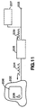
- figure 11 shows a video monitor 202 having a display screen 206 suitable for displaying images 208 rendered from digital video 204.
- the source of digital video 204 is video decoder 205.
- Video decoder 205 includes suitable decoding circuitry (not shown).
- Video decoder 205 decodes encoded video 209. Typical sources of encoded video 209 include CD or laser disc player 207, or cable television hook-up 208.
- FIG 5 there is shown a portion of a display screen 206, including image 208.
- Images such as image 208 are composed of pixels 214.
- pixels 214 are grouped into cells 212.
- the digital video 204 representing image 208 (as well as the reset of display screen 6) can be manipulated (e.g., compressed) more efficiently.
- cells 212 could be arranged in any repeating pattern, typically cells 212 are arranged in the pattern of a rectilinear grid 209. The pattern of grid 209 extends across display screen 206.
- pixels 214 typically are arranged in a square matrix of N rows by N columns. For example, in figure 6 cell 212 consists of eight row by eight columns of pixels 214. Associated with each pixel 214 is an identifying position number 13 (from 0 to 63). Alternately, pixels 214 could be grouped in a non-square matrix (i.e., M rows by N columns, where M does not equal N).
- digital video 204 includes a number of data words 215.
- six data words 215 are required to represent each region of four pixels 214:
- One word 215 represents Cb
- one word 215 represents Cr
- four words 215 represent Y (luminance).
- video decoder 205 includes RAM system 230.
- RAM system 230 is the memory video decoder 205 uses to store data words 215.
- Video decoder 205 reads words 215 from RAM system 230 in the course of creating, displaying, and manipulating image 208 on screen 206.
- RAM system 230 includes interleaver 234 and two banks 232 of RAM, bank0 232-0 and bank1 232-1, interleaver 234 connects banks 232 to the portion (not shown) of video decoder 205 that is used to create, display, and manipulate images 206.
- data words 215 are stored in pages 233, which are represented in figure 10 as overlapping rectangles.
- a typical size for a page 233 is 1024 eight bit words.
- one requirement of video decoder 205 is the ability to read a cell 222 that is not aligned to the existing cell grid 209. Instead, cell 222 is aligned to pixels 214 within cells 212. This ability to read unaligned cells 222 is required for searching image 208 for features, or for detecting motion between successive images 208.
- FIG. 222-1 there is shown a cell 222-1 to be read from RAM system 230.
- Cell 222-1 is not aligned with grid 209, but is aligned to the pixels 214 of cells 212.
- Cell 222-1 is shown in dotted lines, and can be seen to overlap four cells 212, 212-5, 212-6, 212-7, and 212-8.
- unaligned read cell 222-1 overlaps underlying cells 212-5, 212-6, 212-7 and 212-8.
- the numbers 28 within cell 222-1 represent the numbers 13 of the pixels 214 at the boundary between cell 222-1 and each underlying cell 212.
- unaligned read cell 222-1 largely consists of pixels 214 drawn from a single underlying cell 212-5.
- the number of pixels 214 drawn from cells 212-6, 212-8, and 212-7 are seven, seven and one, respectively. Forty-nine pixels are drawn from cell 212-5.
- rectilinear grid 209 is shown without showing how pages 233 containing the data words 215 representing each cell 212 are interleaved.
- the respective pages 233 associated with all of the cells 212 underneath a particular unaligned read cell 222 could be in the same bank 232 of RAM system 230. If so, creating the unaligned read cell 222 would, in the worst case, involve accessing four pages 233 from the same bank 232, a process that required dead time to precharge that bank 232 three times. For all unaligned cells 222 on image 8, the worst case must appear: Searching or matching do not specify where unaligned cell 222 is, and hence can always be the worst case.
- the problem of relatively short read times is reduced by interleaving in a particular two-dimensional pattern 240 the pages 233 associated with cells 212.
- FIG 9 half of the cells 212 are shown with hatching 239, and half of the cells 212 lack hatching 239.
- the presence of hatching 239 on a cell 212 signifies that the page 233 associated with that particular cell 212 resides in bank0 232-0.
- the absence of hatching 239 on a cell 212 signifies that the page 233 associated with that particular cell 212 resides in bank1 232-1.
- cell 212-6 is shown hatched, so the page 233 associated with the data words 215 that describe cell 212-6 are stored in bank0 232-0, and so must be read from bank0 232-0.
- interleaver 234 interleave pages 233 into banks 232 based on a particular two dimensional pattern 240 of cells 212 associated with pages 233.
- pattern 240 resembles a checkerboard: No two sequential cells 212 in the same row of grid 209 have their associated page 233 in the same bank 232, and no two sequential cells 212 in the same column of grid 209 have their associated page 233 in the same bank 232.
- Checkerboard pattern 240 maximizes interleave possibilities by ensuring that when unaligned read cell 222 overlies four cells 212, the pages 233 of two of the overlaid cells 212 are stored in one bank 232, while the pages 233 associated with the other two overlaid cells 212 are stored in the other bank 232. For example, in figure 9, cells 212-5 and 12-7 have their associated pages 233 stored in bank1 232-1, while cells 212-6 and 12-8 have their associated pages 233 stored in bank0 232-0.
- pages 233 should be read from alternate banks 232. This is ensured by reading from the four cells 212 underlying an unaligned read cell 222 in either a clockwise order, or in a counter-clockwise order.
- the method of reading in the clockwise direction consider the four cells 212 underlying cell 222-1 in figure 9.
- the page 233 associated with cell 212-5 would be read from bank1 232-1 by interleaver 234.
- the page 233 associated with cell 212-6 would be read, since cell 212-6 is positioned in the same row as cell 212-5, and to the right of cell 212-5.
- checkerboard pattern 240 of interleaving banks 232 reduces dead time.
- the aspect ratio and size of checkerboard pattern 240 can be selected to be optimum for the particular application.
- the only requirement is that at least one cell 212 underlying an unaligned read cell 222 is represented by less than one page 233 or words 215. In this manner, each of the four possible reads of underlying cells 212 is self-contained, limiting the interleaving to the mechanism described. Any further fragmentation would involve a more complex interleaving algorithm and would cause longer dead times.
- each pair of possible reads of underlying cells 212 contains words 215 in the same page 233 (e.g., words 215 from cells 212-6 and 212-8 underlying unaligned read cell 222-1 many be contained on the same page 233). Therefore the reading of words 215 from pages 233 could be further optimized. However, the worst case scenario remains.
- the method of the present invention can also be applied, with out any loss in performance, to cells 212 having dimensions (M by N) that require more data words 215 than can be stored in a single page 233.
- a cell 212 is divided by subgrid 252 into subcells 250, with the dimensions of subcells 250 chosen so that the number of words 215 associated with each subcell 250 can be stored in a single page 233.
- the same checkerboard pattern 240 can be applied to subcells 50 (e.g., subcells 250-1 and 250-3 stored in the same bank 232, and subcells 50-2 and 50-4 stored in the same bank 232), allowing the accessing of words 215 associated with each "oversized" cell 212 to be managed in the same efficient manner as cells 212 themselves are managed.
- subcells 50 e.g., subcells 250-1 and 250-3 stored in the same bank 232, and subcells 50-2 and 50-4 stored in the same bank 232
- a method and apparatus for addressing memory is described herein.
- the process calls for using a fixed width word for addressing variable width data.
- the fixed width word may contain a width defining field, an address field, or a substitution field.
- the length of the fixed width word is predetermined by the amount of memory to be addressed.
- the apparatus form of the present invention includes a microcodable state machine with an arithmetic core.
- the microcodable state machine is intended to be used to solve design problems where there is a need for versatile and/or complicated calculations. Examples of such designs are; address generation, stream parsing and decoding or filter tap coefficient calculations.
- the addressing must cope with two different features, variable length addresses to access varying width portions of words and address substitution.
- a RAM having a 64 x 32 bit configuration can be addressed in partial words having 64 x 32 bit, 128 x 16 bit, 256 x 8 bit, 512 x 4 bit, 1024 x 2 bit, or 2048 x 1 bit formats.
- variable portions of a word to be known as fields
- actions such as substitution, variable width data addressing, or the constriction of other parts of the word.
- the conventional method for this would be to have an additional word (or words) to specify the width of the field (or fields) within the word.
- an additional word or words
- This method has the advantages of saving bits in the overall definition of the word, simplifying decoding of the encoded word and providing a more intuitive view of what has been encoded.
- This encoding method is applicable if the variable width fields are most or least significant bit justified within the word.
- Table 1-1 shows two examples of variable width fields (marked “F") least significant bit justified defined within a eight bit word, "w” marks other potential fields of these words.
- Table 1-2 shows the conventional method of encoding the fields shown in Table 1-1 by the addition of enough bits to specify the maximum width of the field in binary. (Bits marked “x” are "don't care” - a term of art). Too much space is taken up with this method.
- Table 1-3 show the encoding of the fields shown Table 1-1 using the new method.
- This method defines the field by the using a continuation marker and a termination marker.
- the continuation marker is "1" and the termination marker is "0".
- the field is defined as all continuation markers from the justified end of the field (least significant in this case) until and including the termination marker. It is shown in Table 1-3 that to encode the field the space taken by a termination marker must be added to the fixed width word at the start of the field, this allows the definition of a zero length field by the additional space containing a termination marker.
- Fields may also be most significant bit justified such as shown in Table 1-5. These are encoded in a similar way to least significant bit justified fields simply that the field reaches from the most significant bit (hereinafter MSB) towards the least significant bit (hereinafter "LSB") up to and including the first termination marker.
- MSB most significant bit
- LSB least significant bit
- Table 1-6 The encoding of the fields shown in Table 1-5 are shown in Table 1-6.
- An address field not necessarily used to address data has a field having a termination marker and a continuation marker. In this case the field is least significant bit justified.
- Table 1-9 show the encoding for substitution into a 1 2 bit address.
- a fixed width word for addressing having an address field with an optional substitution indicator.
- the substitution field has a variable size and will function to substitute an outside addressing source for a variable amount of address bits "a”. The substitution occurs in place of the termination marker bits(s) "y" and continuation marker bit(s) "x".
- the termination marker functions to inform the address decoding circuit where the substitution stops.
- the continuation marker pads the fixed width word.
- substitution indicator allows optimal use of substitution.
- One embodiment of the present invention is for addressing a memory which can be accessed at it full width or in 2 n widths up to its full width (these smaller words are called partial words). It will be shown how the variable field encoding can be used to address this memory and to index those addresses into the memory.
- substitution portion (or field) of the address can be defined by a least significant bit justified variable length field (The continuation marker “1", termination marker "0") that is super imposed on top of those shown in Table 1-10.
- Table 1-11 shows how to define the number of the least significant bits to be substituted.
- the least significant bit added is the substitution indicator (marked "w").
- the general case of a Fixed width word for substitution is shown in Figure 20. In effect the substitute code is superimposed on top of the address that is already coded.
- the apparatus for addressing and a method for accessing partial words in a register file will be discussed below.
- the conventional memory circuitry dictates that the memory must always be accessed at its full width.
- a full (32 bit) width word is read. This full word is rotated until the partial word accessed is justified in the LSB.
- the upper parts of the word are extended to the full width and then output. Extending may encompass padding with zeros or ones, sign extending, using the sign bit of a sign-magnitude number as the new MSB or any similar conventional method. Extending is dependent on the mode of operation.
- Figure 15 show these steps for the access of a 4 bit partial word in the fourth four bitword of the 32 bit word.
- the full width word must be rotated to place the partial word at the LSB, as shown in row "2". As shown in row "3" the four bit word is extended to create a create full 32 bit word. This word can now be accessed.
- a full width word that has been selected to be written back is truncated to the width of the original partial word which is multiplexed into the word shown in row "2" at the LSB position, this is shown in row "4".
- the resulting word is rotated back in its original significance in the read word, this is shown in row "5". This full word can now be written back into the register file.
- the memory address must be decoded to control the above structure. It should be recognized that the MSB of any width of address is at the same significance with reference to the memory.
- the top six bits of a decoded address are a 32 bit word address, the remainder is a bit address. Therefore the stage of decoding (in parallel with the substitution) is to decode the address width defining variable field by detecting the position of the most significant termination marker. This allowing the address to be MSB justified (shifting in zeros at the LSB).
- the top six bits can be used directly as a 32 bit word row address the memory.
- the bottom five bits can be used to directly control both barrel shifters (as seen in Figure 16), because for example an original 32 bit address will always have a shift of 0b00000 (these having been shifted when the address was MSB justified) similarly a 16 bit address can have a shift of 0bx0000 i.e. 0 or 16 bit shift and a 1 bit address can have a shift of Obxxxxx i.e. 0 to 31 bit shifts.
- the extender and input multiplexer are controlled by the access width decode to mask out the output words and multiplex the input words to an appropriate significance respectively.
- the block diagram of the decode is shown in Figure 17. It can be seen that the decode of the two variable width fields for width and substitution can be done in parallel and independently.
- Figure 20 represents an example of fixed width word 13 bits long for addressing variable width data and substitution as shown in the bottom two rows. For these examples an eight bit word would have been addressed at location 0b1101ssss, where "ssss" is substituted from another address source.
- the substitution into a memory address and variable width accessing of a memory have been brought together in the implementation of a microcodable state machine the structure of which is shown in Figure 13.
- the structure is one of a state machine controlling an arithmetic core by way of a wide word of control signals called a microcode instruction.
- the arithmetic core passes status flags and some data to the state machine.
- the state machine consists of a memory containing a list of the microcode instructions. As with conventional microcodable state machines it is capable of either proceeding through the list of microcode instructions contiguously or any instruction can jump to any other.
- the jump address is in the form of Figure 19.
- the value substituted comes from the arithmetic core as shown in Figure 13 and 14. This allows the construction of "jump tables" within the micro code programs. Thus if a jump is made with 3 bits substituted, for example, there are a possible eight contiguous locations that may be jumped to dependent on the value from the arithmetic core, it has so become a programmable jump.
- the arithmetic core is composed of a memory called a register file, an Arithmetic and Logic Unit (ALU), an input port and output port. These components are connected by busing and multiplexers. As previously stated these and the multiplexers defining their connections are entirely controlled by the microcode instruction issued by the state machine.
- the ALU and ports are conventional, but the register file is a memory that allows variable width index accesses to it. The address to the register file is coded directly into the microcode instruction.
- a procedure for addressing memory having the following steps: providing a fixed width word having a predetermined fixed number of bits to be used for addressing variable width data, defining the fixed width word with a width defining field and an address field providing the width defining field with at least one bit to serve as the termination marker, defining the address field with a plurality of bits defining the address of the data, varying the size of bits in the address field in inverse relation to the size of the variable width data, varying the number of bits in the width defining field in direct relation to the size of the variable width data and maintaining a fixed width word for addressing variable width data while varying the width of the width defining field and the address field.
- a procedure for addressing memory having the following steps: providing a fixed width word having a predetermined fixed number of bits to be used for addressing data, defining the fixed width word with an address field and a substitution field 1 defining the address field with a plurality of bits defining the address of the data, defining a variable width substitution field with at least one substitution bit, the substitution field has at least one bit to serve as a termination marker between the address field and the substitution field, using the substitution field to indicate substituted bits from a separate addressing source and maintaining a fixed width word for addressing variable width data while inversely varying the width of the address field and the width of the substitution field.
- a process for addressing variable width data in a memory having the following steps providing a memory having words of predetermined width and composed of partial words, rotating the partial word to be accessed to a least significant bit justification, extending remaining part of the word so that the accessed word will be recognized as the partial word, restoring the remaining part of the word and rotating the word until the partial word is restored to its original position.
- An image formatter is shown in Figure 24.
- Tokens arriving at the input to the image formatter are buffered in the FIF0 440 and transferred into the buffer manager 430.
- This block detects the arrival of new pictures and determines the availability of a buffer in which to store each one. If there is a buffer available, it is allocated to the arriving picture and its index is transferred to the write address generator 410. If there is no buffer available, the incoming picture will be stalled until one does become free. All tokens are passed on to the write address generator 410. This operation is described in greater details in U.K. Serial No. 9405914.4 filed on March 24, 1994, which is incorporated herein by reference.
- External DRAM is used for the buffers, which can be either two or three in number. Three are necessary if frame-rate conversion is to be effected.
- the purpose of the buffer manager 430 is to supply the address generators with indices indicating any of either two or three external buffers for writing and reading of picture data.
- the allocation of these indices is influenced by three principal factors, each representing the effect of one of the timing regimes in operation: the rate at which picture data arrives at the input to image formatter (coded data rate), the rate at which data is displayed (display data rate), and the frame rate of the encoded video sequence (presentation rate).
- a three-buffer system enables the presentation rate and the display rate to differ (e.g. 2-3 pulldown), so that frames are either repeated or skipped as necessary to achieve the best possible sequence of frames given the timing constraints of the system. Pictures which present some difficulty in decoding may also be accommodated in a similar way, so that if a picture takes longer than the available display time to decode, the previous frame will be repeated which everything else 'catches up'. In a two-buffer system the three timing regimes must be locked - it is the third buffer which provides the flexibility for taking up slack.
- the buffer manager operates by maintaining certain status information associated with each external buffer - this includes flags indicating if the buffer is in use, full of data, or ready for display, and the picture number within the sequence of the picture currently stored in the buffer.
- the presentation number is also recorded, this being a number which increments every time a picture dock pulse is received, and represents the picture number which is currently expected for display based on the frame rate of the encoded sequence.
- An arrival buffer (a buffer to which incoming data will be written) is allocated every time a PICTURE_ START token is detected at the input, and this buffer is then flagged as IN_USE; on PICTURE_END, the arrival buffer will be de-allocated (reset to zero) and the buffer flagged as either FULL or READY depending on the relationship between the picture number and the presentation number.
- the display address generator requests a new display buffer, once every vsync, via a two-wire-interface. If there is a buffer flagged as READY, then that will be allocated to display by the buffer manager. If there is no READY buffer, the previously displayed buffer will be repeated.
- TEMPORAL_REFERENCE tokens in H261 cause a buffer's picture number to be modified if skipped pictures in the input stream are indicated.
- TEMPORAL_REFERENCE tokens in MPEG have no effect.
- a FLUSH token causes the input to stall until every buffer is either EMPTY or has been allocated as the display buffer; presentation number and picture number are then reset and a new sequence can commence.
- All data is input to the buffer manager from the input fifo, bm_front. This transfer takes place via a two-wire interface, the data being 8 bits wide plus an extension bit. All data arriving at the buffer manager is guaranteed to be complete tokens, a necessity for the continued processing of presentation numbers and display buffer requests in the event of significant gaps in the data upstream.
- Tokens (8 bit data, 1 bit extension) are transferred to the write address generator via a two-wire interface.
- the arrival buffer index is also transferred on the same interface, so that the correct index is available for address generation at the same time as the PICTURE_START token arrives at waddrgen.
- the interface to the read address generator comprises two separate two-wire interfaces which can be considered to act as 'request' and 'acknowledge' signals respectively - single wires are not adequate, however 1 because of the two two-wire-based state machines at either end.
- dispeddr invokes a request, in response to a vsync from the display device, by asserting the drq_valid input to the buffer manager; when the buffer manager reaches an appropriate point in its state machine it will accept the request and go about allocating a buffer to be displayed; the disp_valid wire is then asserted, the buffer index is transferred, and this will normally be accepted immediately by dispaddr.
- rst_fld There is an additional wire associated with this last two-wire-interface (rst_fld) which indicates that the field number associated with the current index must be reset regardless of the previous field number.
- the buffer manager block uses four bits of microprocessor address space, together with the 8-bit data bus and read and write strobes. There are two select signals, one indicating user-accessible locations and the other indicating test locations which should not require access under normal operation conditions.
- the buffer manager is capable of producing two different events: index found and late arrival. The first of] these is asserted when a picture arrives whose PICTURE_START extension byte (picture index) matches the value written into the BU_BM_TARGET_IX register at setup. The second event occurs when a display buffer is allocated whose picture number is less than the current presentation number, i.e. the processing in the system pipeline up to the buffer manager has not managed to keep up with the presentation requirements.
- Picture clock is the clock signal for the presentation number counter and is either generated on-chip or taken from an external source (normally the display system).
- the buffer manager accepts both of these signals and selects one based on the value of pclk_ext (a bit in the buffer manager's control register). This signal also acts as the enable for the pad picoutpad, so that if the image Formatter is generating its own picture clock this signal is also available as an output from the chip.
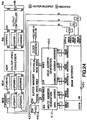
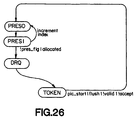
- the reset state is PRESO, with flags set to zero such that the main loop is circulated initially.
- the main loop of the state machine comprises the states shown in Figure 26 (highlighted in the main diagram - Figure 25).
- States PRESO and PRES1 are concerned with detecting a picture dock via the signal presflg. Two cycles are allowed for the tests involved since they all depend on the value of rdytst. If a presentation flag is detected, all of the buffers are examined for possible 'readiness', otherwise the state machine just advances to state DRQ.
- State DRQ checks for a request for a display buffer (drq_valid_reg && disp_acc_reg). If there is no request the state advances (normally to state TOKEN - more on this later), otherwise a display buffer index is issued as follows: If there is no ready buffer, the previous index is re-issued or, if there is no previous display buffer. a null index (zero) is issued; if a buffer is ready for display, its index is issued and its state is updated - if nec_ essary the previous display buffer is cleared. The state machine then advances as before.
- State TOKEN is the usual option for completing the main loop: if there is valid input and the output is not stalled, tokens are examined for strategic values (described in later sections), otherwise control returns to state PRES0.
- Control only diverges from the main loop when certain conditions are met.
- any previous ready buffer needs to be vacated because only one buffer can be designated ready at any time.
- State VACATE_RDY clears the old ready buffer by setting its state to VACANT, and it resets the buffer index to 1 so that when control returns to the PRES0 state, all buffers will be tested for readiness. The reason for this is that the index is by now pointing at the previous ready buffer (for the purpose of clearing it) and there is no record of our intended new ready buffer index - it is necessary therefore to re-test all of the buffers.
- Allocation of the display buffer index takes place either directly from state DRQ (state USE_RDY) or via state VACATE_DISP which clears the old display buffer state.
- the chosen display buffer is flagged as IN_USE, the value of rdy_buf is set to zero, and the index is reset to 1 to return to state DRQ.
- disp_buf is given the required index and the two-wire interface wires (disp_valid and drq_acc) are controlled accordingly. Control returns to state DRQ only so that the decision between states TOKEN, FLUSH and ALLOC does not need to be made in state USE_RDY.
- the en_full signal is supplied by the write address generator to indicate that the swing buffer has swung, i.e. the last block has been successfully written and it is therefore safe to update the buffer status.
- the just-completed buffer is tested for readiness and given the status either FULL or READY depending on the result of the test. If it is ready, rdy_buf is given the value of its index and the set_la_ev signal (late arrival event) is set high (indicating that the expected display has got ahead in time of the decoding). The new value of arr_buf now becomes zero, and, if the previous ready buffer needs its status clearing, the index is set to point there and control moves to state VACATE_RDY; otherwise index is reset to 1 and control returns to the start of the main loop.
- State ALLOC is concerned with allocating an arrival buffer (into which the arriving picture data can be written), and cycles through the buffers until it finds one whose status is VACANT. A buffer will only be allocated if out_acc_reg is high, since it is output on the data two-wire-interface, so cycling around the loop will continue until this is the case. Once a suitable arrival buffer has been found, the index is allocated to arr_buf and its status is flagged as IN_USE.
- Index is set to 1, the flag from_ps is reset, and the state is set to advance to NEW_EXP_TR.
- a check is made on the picture's index (contained in the word following the PICTURE_START) to determine if it the same as targ_ix (the target index specified at setup) and, if so, set_if_ev (index found event) is set high.
- the three states NEW_EXP_TR, SET_ARR_IX and NEW_PIC_NUM set up the new expected temporal reference and picture number for the incoming data - the middle state just sets the index to be arr_buf so that the correct picture number register is updated (note that this_pnum is also updated).
- Control then goes to state OUTPUT_TAIL which outputs data (assuming favourable two-wire interface signals) until a low extension is encountered, at which point the main loop is re-started. This means that whole data blocks (64 items) are output, within which there are no tests for presentation flag or display request.
- a FLUSH token in the data stream indicates that sequence information (presentation number, picture number, rst_fld) should be reset. This can only happen when all of the data leading up to the FLUSH has been correctly processed and so it is necessary, having received a FLUSH, to monitor the status of all of the buffers until it is certain that all frames have been handed over to the display, i.e. all but one of the buffers have status EMPTY, and the other is IN_USE (as the display buffer). At that point a 'new sequence' can safely be started.
- state TOKEN When a FLUSH token is detected in state TOKEN, the flag from_fl is set, causing the basic state machine loop to be changed such that state FLUSH is visited instead of state TOKEN.
- State FLUSH examines the status of each buffer in turn, waiting for it to become VACANT or IN_USE as display. The state machine simply cycles around the loop until the condition is true, then increments its index and repeats the process until all of the buffers have been visited. When the last buffer fulfils the condition, presentation number, picture number and all of the temporal reference registers assume their reset values; rst_fld is set to 1. The flag from_fl is reset and the normal main loop operation is resumed.
- State TOKEN passes control to state OUTPUT_TAIL in all cases other than those outlined above. Control remains here until the last word of the token is encountered (in_extn_reg is low) and the main loop is then reentered.
- a typical sequence of states may be PRES0, PRES1, DRQ, TOKEN, OUTPUT_TAIL, each, with the exception of OUTPUT_TAIL, lasting one cycle.
- This number may occasionally increase to up to 13 cycles overhead when auxiliary branches of the state machine are executed under worst-case conditions. Note that such large overheads will only apply on a once-per-frame basis.
- Presentation number free-runs during upi accesses if presentation number is required to be the same when access is relinquished as it was when access was gained, this can be effected by reading presentation number after access is granted, and writing it back just before it is relinquished. Note that this is asynchronous, so it may be necessary to repeat the accesses several times to be sure they are effective.
- the write address generator 410 receives tokens from the buffer manager 430 and detects the arrival of each new DATA token. As each arrives, it calculates a new address for the DRAM interface 450 in which to store the arriving block. The raw data is then passed to the DRAM interface 450 where it is written in to a swing buffer.
- DRAM addresses are block addresses, and pictures in the DRAM are organised as rasters of blocks. Incoming picture data, however, is organised as sequences of macroblocks, so the address generation algorithm must take account of this.
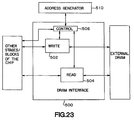
- a single high performance, configurable DRAM interface 500 is illustrated in Fig. 22.
- This interface is a standard-independent block and is designed to directly drive the DRAMs required, for example, by a spatial decoder, a temporal decoder and a video formatter. No external logic, buffers or components will be required to connect the DRAM interface to DRAM in those systems.
- the interface is configurable in two ways. First, the detailed timing of the interface can be configured to accommodate a variety of different DRAM types. Second, the width of the data interface to the DRAM can be configured to provide a cost/performance trade-off for different applications.
- the DRAM interface connects the chip to external DRAM.
- External DRAM is used, because at present, it is not practical to fabricate on the chips the relatively large amount of DRAM needed. However, it is possible to fabricate on the chips the large amount of DRAM that is needed.
- DRAM interface is standard-independent, it still must be configured to implement each of the multiple standards, H.261, JPEG and MPEG. How the DRAM interface is reconfigured for multi-standard operation is discussed further herein.
- DRAM interface 500 An important aspect in understanding the operation of the DRAM interface 500 is to understand the relationship between the DRAM interface 500 and the address generator 510, and how the two communicate using the two wire interface.
- a buffer manager 540 supervises the two address generators 520 and 530. This buffer manager 540 is described in greater detail elsewhere in this application.
- the address generator generates the addresses the DRAM interface needs to address the DRAM (e.g., to read from or to write to a particular address in DRAM).
- the DRAM interface e.g., to read from or to write to a particular address in DRAM.
- reading and writing only occurs when the DRAM interface has both data (from preceding stages in the pipeline), and a valid address (from address generator).
- address generator simplifies the construction of both the address generator and the DRAM interface, as discussed further below.
- the DRAM interface can operate from a clock which is asynchronous to both the address generator and to the clocks of the blocks which data is passed from and to. Special techniques have been used to handle this asynchronous nature of the operation.
- swing buffer This is essentially a pair of RAMs operated in a double-buffered configuration, with the DRAM interface filling or emptying one RAM while another part of the chip empties-or fills the other RAM.
- a separate bus which carries an address from an address generator is associated with each swing buffer.
- Each of the chips has four swing buffers, but the function of these swing buffers is different in each case.
- one swing buffer is used to transfer coded data to the DRAM, another to read coded data from the DRAM, the third to transfer tokenised data to the DRAM and the fourth to read tokenised data from the DRAM.
- one swing buffer is used to write intra or predicted picture data to the DRAM, the second to read intra or predicted data from the DRAM and the other two to read forward and backward prediction data.
- one swing buffer issued to transfer data to the DRAM and the other three are used to read data from the DRAM, one for each of the luminance (Y) and the red and blue colour difference data (Cr and Cb).
- a control 506 interfaces between the address generator 510, the DRAM interface 500, and the remaining blocks of the chip which supply and take the data are all two wire interfaces
- the address generator 510 may either generate addresses as the result of receiving control tokens, or it may merely generate a fixed sequence of addresses.
- the DRAM interface 500 treats the two wire interfaces with the address generator 510 in a special way. Instead of keeping the accept line high when it is ready to receive and address, it waits for the address generator to supply a valid address, processes that address, and then sets the accept line high for one clock period. Thus it implements a request/acknowledge (REQ/ACK) protocol.
- REQ/ACK request/acknowledge
- a unique feature of the DRAM interface 500 is its ability to communicate independently with the address generator 510 and with the blocks which provide or accept the data.
- the address generator 510 may generate an address associated with the data in the write swing buffer 502, but no action will be taken until the write swing buffer 502 signals that there is a block of data ready to be written to the external DRAM.
- the write swing buffer 502 may contain a block of data which is ready to be written to the external DRAM, but no action is taken until an address is supplied on the appropriate bus from the address generator 510. Further, once one of the RAMs in the write swing buffer 502 has been filled with data, the other may be completely filled and "swung" to the DRAM interface side before the data input is stalled (the two-wire interface accept signal set low).
- the DRAM interface 500 will be able to transfer data between the swing buffers 502 and 504 and the external DRAM at least as fast as the sum of all the average data rates between the swing buffers 502 and 504 and the rest of the chip.
- Each DRAM interface 500 contains a method of determining which swing buffer it will service next. In general, this will either be a "round robin" (i.e. the swing buffer which is serviced is the next available swing buffer which has least recently had a turn) or a priority encoder, (i.e. in which some swing buffers have a higher priority than others). In both cases, an additional request will come from a refresh request generator which has a higher priority than all the other requests. The refresh request is generated from a refresh counter which can be programmed via a microprocessor interface.
- the write swing buffer interface two blocks of RAM, RAM1 and RAM2.
- data is written into RAM 1 and RAM 2 from the previous block or stage, under control of the write address and control. From RAM1 and RAM 2, the data is written into DRAM.
- the DRAM row address is provided by the address genrator, and the column address is provided by the write address and control, as described further herein.
- valid data is presented at the input (data in). The data is received from the previous stage.
- the write address control increments the RAM1 address to allow the next place of data to be written into RAM1.
- Data continues to be written into RAM1 until either there is no more data, or RAM1 is full.
- the input side gives up control and sends a signal to the read side to indicate that RAM1 is now ready to be read. This signal passes between two asynchronous clock regimes, and so passes through three synchronizing flip flops.
- RAM2 is empty, the next item of data to arrive on the input side is written into RAM2, otherwise, this occurs when RAM2 has emptied.
- the round robin or priority encoder (depending on which is used by the particular chip) indicates that it is the turn of this swing buffer to be read, the DRAM interface reads the contents of RAM1 and writes them to the external DRAM. A signal is then sent back across the asynchronous interface, to indicate that RAM1 is now ready to be filled again.
- the DRAM interface 500 is designed to maximize the available memory bandwidth. Each 8x8 block of data is stored in the same DRAM page. In this way, full use can be made of DRAM fast page access modes, where one row address is supplied followed by many column addresses. In particular, row addresses are supplied by the address generator 510, while column addresses are supplied by the DRAM interface 500, as discussed further below.
- the facility is provided to allow the data bus to the external DRAM to be 8, 16 or 32 bits wide, so that the amount of DRAM used can be matched to size and bandwidth requirements of the particular application.
- the address generator 510 provides the DRAM interface 500 with block addresses for each of the read and write swing buffers 505 and 502. This address is used as the row address for the DRAM.
- the six bits of column address are supplied by the DRAM interface itself, and these bits are also used as the address for the swing buffer RAM.
- the data bus to the swing buffers is 32 bits wide so if the bus width to the external DRAM is less than 32 bits, two or four external DRAM accesses must be made before the next word is read from a write swing buffer or the next word is written to a read swing buffer (read and write refer to the direction of transfer relative to the external DRAM).
- DRAM interface 500 is not limited to two swing buffers.
Landscapes
- Engineering & Computer Science (AREA)
- Theoretical Computer Science (AREA)
- Physics & Mathematics (AREA)
- General Engineering & Computer Science (AREA)
- General Physics & Mathematics (AREA)
- Multimedia (AREA)
- Signal Processing (AREA)
- Mathematical Physics (AREA)
- Dram (AREA)
- Information Transfer Systems (AREA)
- Executing Machine-Instructions (AREA)
- Diaphragms For Electromechanical Transducers (AREA)
- Television Systems (AREA)
- Debugging And Monitoring (AREA)
Applications Claiming Priority (11)
| Application Number | Priority Date | Filing Date | Title |
|---|---|---|---|
| GB9405914 | 1994-03-24 | ||
| GB9405914A GB9405914D0 (en) | 1994-03-24 | 1994-03-24 | Video decompression |
| GB9415391A GB9415391D0 (en) | 1994-07-29 | 1994-07-29 | Method for accessing banks of dram |
| GB9415413 | 1994-07-29 | ||
| GB9415387 | 1994-07-29 | ||
| GB9415391 | 1994-07-29 | ||
| GB9415365A GB9415365D0 (en) | 1994-07-29 | 1994-07-29 | Method for accessing ram |
| GB9415387A GB9415387D0 (en) | 1994-07-29 | 1994-07-29 | Method and apparatus for addressing memory |
| GB9415365 | 1994-07-29 | ||
| GB9415413A GB9415413D0 (en) | 1994-07-29 | 1994-07-29 | Method and apparatus for video decompression |
| EP95301272A EP0674266A3 (de) | 1994-03-24 | 1995-02-28 | Verfahren und Vorrichtung zur Schnittstellenbildung mit RAM-Speicher |
Related Parent Applications (1)
| Application Number | Title | Priority Date | Filing Date |
|---|---|---|---|
| EP95301272A Division EP0674266A3 (de) | 1994-03-24 | 1995-02-28 | Verfahren und Vorrichtung zur Schnittstellenbildung mit RAM-Speicher |
Publications (2)
| Publication Number | Publication Date |
|---|---|
| EP0895166A2 true EP0895166A2 (de) | 1999-02-03 |
| EP0895166A3 EP0895166A3 (de) | 1999-03-10 |
Family
ID=27517237
Family Applications (6)
| Application Number | Title | Priority Date | Filing Date |
|---|---|---|---|
| EP98202091A Ceased EP0895166A3 (de) | 1994-03-24 | 1995-02-28 | Verfahren und Vorrichtung zur Schnittstellenbildung mit RAM-Speicher |
| EP98202090A Withdrawn EP0895422A3 (de) | 1994-03-24 | 1995-02-28 | Bildformatierer zur Verarbeitung von kodierten Videodaten |
| EP00201754A Expired - Lifetime EP1026600B1 (de) | 1994-03-24 | 1995-02-28 | Verfahren und Vorrichtung zur Schnittstellenbildung mit RAM-Speicher |
| EP98202093A Ceased EP0895161A3 (de) | 1994-03-24 | 1995-02-28 | Verfahren zur Adressierung von Speicherdaten mit veränderlichen Breiten |
| EP95301272A Withdrawn EP0674266A3 (de) | 1994-03-24 | 1995-02-28 | Verfahren und Vorrichtung zur Schnittstellenbildung mit RAM-Speicher |
| EP98202092A Withdrawn EP0895167A3 (de) | 1994-03-24 | 1995-02-28 | Verfahren und Vorrichtung zur Schnittstellenbildung mit RAM-Speicher |
Family Applications After (5)
| Application Number | Title | Priority Date | Filing Date |
|---|---|---|---|
| EP98202090A Withdrawn EP0895422A3 (de) | 1994-03-24 | 1995-02-28 | Bildformatierer zur Verarbeitung von kodierten Videodaten |
| EP00201754A Expired - Lifetime EP1026600B1 (de) | 1994-03-24 | 1995-02-28 | Verfahren und Vorrichtung zur Schnittstellenbildung mit RAM-Speicher |
| EP98202093A Ceased EP0895161A3 (de) | 1994-03-24 | 1995-02-28 | Verfahren zur Adressierung von Speicherdaten mit veränderlichen Breiten |
| EP95301272A Withdrawn EP0674266A3 (de) | 1994-03-24 | 1995-02-28 | Verfahren und Vorrichtung zur Schnittstellenbildung mit RAM-Speicher |
| EP98202092A Withdrawn EP0895167A3 (de) | 1994-03-24 | 1995-02-28 | Verfahren und Vorrichtung zur Schnittstellenbildung mit RAM-Speicher |
Country Status (3)
| Country | Link |
|---|---|
| EP (6) | EP0895166A3 (de) |
| AT (1) | ATE278988T1 (de) |
| DE (1) | DE69533630T2 (de) |
Families Citing this family (13)
| Publication number | Priority date | Publication date | Assignee | Title |
|---|---|---|---|---|
| US6336180B1 (en) | 1997-04-30 | 2002-01-01 | Canon Kabushiki Kaisha | Method, apparatus and system for managing virtual memory with virtual-physical mapping |
| US5821885A (en) * | 1994-07-29 | 1998-10-13 | Discovision Associates | Video decompression |
| EP0793390A3 (de) * | 1996-02-28 | 1999-11-03 | Koninklijke Philips Electronics N.V. | MPEG-Signaldekodierungsvorrichtung |
| AUPO648397A0 (en) | 1997-04-30 | 1997-05-22 | Canon Information Systems Research Australia Pty Ltd | Improvements in multiprocessor architecture operation |
| US6311258B1 (en) | 1997-04-03 | 2001-10-30 | Canon Kabushiki Kaisha | Data buffer apparatus and method for storing graphical data using data encoders and decoders |
| AUPO647997A0 (en) | 1997-04-30 | 1997-05-22 | Canon Information Systems Research Australia Pty Ltd | Memory controller architecture |
| US6674536B2 (en) | 1997-04-30 | 2004-01-06 | Canon Kabushiki Kaisha | Multi-instruction stream processor |
| US6272257B1 (en) | 1997-04-30 | 2001-08-07 | Canon Kabushiki Kaisha | Decoder of variable length codes |
| US6707463B1 (en) | 1997-04-30 | 2004-03-16 | Canon Kabushiki Kaisha | Data normalization technique |
| FR2766937B1 (fr) * | 1997-07-31 | 2001-04-27 | Sqware T | Protocole et systeme de liaison par bus entre elements d'un microcontroleur |
| JP2000010863A (ja) * | 1998-06-24 | 2000-01-14 | Sony Computer Entertainment Inc | 情報処理装置および方法、並びに提供媒体 |
| US6851052B1 (en) * | 1998-12-10 | 2005-02-01 | Telcordia Technologies, Inc. | Method and device for generating approximate message authentication codes |
| US7212440B2 (en) | 2004-12-30 | 2007-05-01 | Sandisk Corporation | On-chip data grouping and alignment |
Family Cites Families (15)
| Publication number | Priority date | Publication date | Assignee | Title |
|---|---|---|---|---|
| JPS53114617A (en) * | 1977-03-17 | 1978-10-06 | Toshiba Corp | Memory unit for picture processing |
| US4135242A (en) * | 1977-11-07 | 1979-01-16 | Ncr Corporation | Method and processor having bit-addressable scratch pad memory |
| GB2039106B (en) * | 1979-01-02 | 1983-03-23 | Honeywell Inf Systems | Number format conversion in computer |
| US4564915A (en) * | 1980-04-11 | 1986-01-14 | Ampex Corporation | YIQ Computer graphics system |
| DE3138897C2 (de) * | 1981-09-30 | 1987-01-08 | Siemens AG, 1000 Berlin und 8000 München | Schaltungsanordnung zum Ausrichten von Speicheroperanden für dezimale und logische Befehle |
| US4800431A (en) * | 1984-03-19 | 1989-01-24 | Schlumberger Systems And Services, Inc. | Video stream processing frame buffer controller |
| JPS6180940A (ja) * | 1984-09-28 | 1986-04-24 | Hitachi Ltd | デ−タ伝送方式 |
| JP2520404B2 (ja) * | 1986-11-10 | 1996-07-31 | 日本電気株式会社 | 圧縮復号化装置 |
| DE3782500T2 (de) * | 1987-12-23 | 1993-05-06 | Ibm | Gemeinsam genutzte speicherschnittstelle fuer datenverarbeitungsanlage. |
| FR2651402B1 (fr) * | 1989-08-22 | 1991-10-25 | Europ Rech Electr Lab | Dispositif de conversion de frequence trame et du nombre de lignes pour un recepteur de television haute definition. |
| KR100214435B1 (ko) * | 1990-07-25 | 1999-08-02 | 사와무라 시코 | 동기식 버스트 엑세스 메모리 |
| US5231605A (en) * | 1991-01-31 | 1993-07-27 | Micron Technology, Inc. | DRAM compressed data test mode with expected data |
| US5265212A (en) * | 1992-04-01 | 1993-11-23 | Digital Equipment Corporation | Sharing of bus access among multiple state machines with minimal wait time and prioritization of like cycle types |
| US5289577A (en) * | 1992-06-04 | 1994-02-22 | International Business Machines Incorporated | Process-pipeline architecture for image/video processing |
| DE69229338T2 (de) * | 1992-06-30 | 1999-12-16 | Discovision Associates, Irvine | Datenpipelinesystem |
-
1995
- 1995-02-28 EP EP98202091A patent/EP0895166A3/de not_active Ceased
- 1995-02-28 EP EP98202090A patent/EP0895422A3/de not_active Withdrawn
- 1995-02-28 EP EP00201754A patent/EP1026600B1/de not_active Expired - Lifetime
- 1995-02-28 EP EP98202093A patent/EP0895161A3/de not_active Ceased
- 1995-02-28 EP EP95301272A patent/EP0674266A3/de not_active Withdrawn
- 1995-02-28 EP EP98202092A patent/EP0895167A3/de not_active Withdrawn
- 1995-02-28 DE DE69533630T patent/DE69533630T2/de not_active Expired - Lifetime
- 1995-02-28 AT AT00201754T patent/ATE278988T1/de not_active IP Right Cessation
Also Published As
| Publication number | Publication date |
|---|---|
| DE69533630T2 (de) | 2005-02-24 |
| DE69533630D1 (de) | 2004-11-11 |
| EP0895166A3 (de) | 1999-03-10 |
| EP0895161A3 (de) | 1999-02-10 |
| EP0674266A2 (de) | 1995-09-27 |
| EP0895422A3 (de) | 1999-03-10 |
| EP1026600A3 (de) | 2000-11-08 |
| EP0895422A2 (de) | 1999-02-03 |
| EP1026600B1 (de) | 2004-10-06 |
| EP0895161A2 (de) | 1999-02-03 |
| ATE278988T1 (de) | 2004-10-15 |
| EP1026600A2 (de) | 2000-08-09 |
| EP0895167A3 (de) | 1999-03-10 |
| EP0674266A3 (de) | 1997-12-03 |
| EP0895167A2 (de) | 1999-02-03 |
Similar Documents
| Publication | Publication Date | Title |
|---|---|---|
| CA2145361C (en) | Buffer manager | |
| US5689313A (en) | Buffer management in an image formatter | |
| RU2134447C1 (ru) | Устройство пересылки данных и видеоигровое устройство, в котором оно используется | |
| US5850632A (en) | Memory access controller utilizing cache memory to store configuration information | |
| US5956744A (en) | Memory configuration cache with multilevel hierarchy least recently used cache entry replacement | |
| US5524265A (en) | Architecture of transfer processor | |
| US5585863A (en) | Memory organizing and addressing method for digital video images | |
| US20140176587A1 (en) | Electronic system and method for selectively allowing access to a shared memory | |
| EP0895166A2 (de) | Verfahren und Vorrichtung zur Schnittstellenbildung mit RAM-Speicher | |
| EP0671718B1 (de) | Datenprozessor für geführte Übertragung zur Zeichnung von Linien | |
| KR100291532B1 (ko) | 리컨피그 가능한 프로세싱 스테이지를 포함하는 정보처리시스템 | |
| US5261049A (en) | Video RAM architecture incorporating hardware decompression | |
| KR100304511B1 (ko) | 비디오복원및디코딩시스템 | |
| EP1880297B1 (de) | Datentransfer-arbitrierungsvorrichtung und datentransfer-arbitrierungsverfahren | |
| EP0671719B1 (de) | Übertragungsprozessor mit Transparenz | |
| EP2382546B1 (de) | Speicherverwaltungsprozess und vorrichtung hierfür | |
| JP3741464B2 (ja) | Dramアクセス方法 | |
| US5861894A (en) | Buffer manager | |
| GB2287808A (en) | Addressing and accessing RAM and data buffering | |
| HK1009611A (en) | Method and apparatus for interfacing with ram | |
| US5686914A (en) | Information processing system | |
| JPH033254B2 (de) | ||
| JPH10144073A (ja) | シンクロナスdramのアクセス機構 | |
| US6865635B1 (en) | Access scheme for a collective resource using a plurality of states | |
| JPH07210693A (ja) | ビデオサブシステムおよびデータ圧縮方法 |
Legal Events
| Date | Code | Title | Description |
|---|---|---|---|
| PUAI | Public reference made under article 153(3) epc to a published international application that has entered the european phase |
Free format text: ORIGINAL CODE: 0009012 |
|
| PUAL | Search report despatched |
Free format text: ORIGINAL CODE: 0009013 |
|
| 17P | Request for examination filed |
Effective date: 19980624 |
|
| AC | Divisional application: reference to earlier application |
Ref document number: 674266 Country of ref document: EP |
|
| AK | Designated contracting states |
Kind code of ref document: A2 Designated state(s): AT BE CH DE FR GB IE IT LI NL |
|
| AK | Designated contracting states |
Kind code of ref document: A3 Designated state(s): AT BE CH DE FR GB IE IT LI NL |
|
| 17Q | First examination report despatched |
Effective date: 20010425 |
|
| GRAG | Despatch of communication of intention to grant |
Free format text: ORIGINAL CODE: EPIDOS AGRA |
|
| RTI1 | Title (correction) |
Free format text: METHOD AND APPARATUS FOR INTERFACING WITH RAM |
|
| STAA | Information on the status of an ep patent application or granted ep patent |
Free format text: STATUS: THE APPLICATION HAS BEEN REFUSED |
|
| 18R | Application refused |
Effective date: 20020902 |