EP0894332B1 - Verwendung verbindungsverfahrens und verbindungsverfahren - Google Patents
Verwendung verbindungsverfahrens und verbindungsverfahren Download PDFInfo
- Publication number
- EP0894332B1 EP0894332B1 EP97915247A EP97915247A EP0894332B1 EP 0894332 B1 EP0894332 B1 EP 0894332B1 EP 97915247 A EP97915247 A EP 97915247A EP 97915247 A EP97915247 A EP 97915247A EP 0894332 B1 EP0894332 B1 EP 0894332B1
- Authority
- EP
- European Patent Office
- Prior art keywords
- process according
- hydrogen
- discharge
- atmosphere
- hlst
- Prior art date
- Legal status (The legal status is an assumption and is not a legal conclusion. Google has not performed a legal analysis and makes no representation as to the accuracy of the status listed.)
- Expired - Lifetime
Links
Images

Classifications
-
- H—ELECTRICITY
- H01—ELECTRIC ELEMENTS
- H01J—ELECTRIC DISCHARGE TUBES OR DISCHARGE LAMPS
- H01J37/00—Discharge tubes with provision for introducing objects or material to be exposed to the discharge, e.g. for the purpose of examination or processing thereof
- H01J37/32—Gas-filled discharge tubes
- H01J37/32431—Constructional details of the reactor
-
- B—PERFORMING OPERATIONS; TRANSPORTING
- B08—CLEANING
- B08B—CLEANING IN GENERAL; PREVENTION OF FOULING IN GENERAL
- B08B7/00—Cleaning by methods not provided for in a single other subclass or a single group in this subclass
- B08B7/0035—Cleaning by methods not provided for in a single other subclass or a single group in this subclass by radiant energy, e.g. UV, laser, light beam or the like
-
- B—PERFORMING OPERATIONS; TRANSPORTING
- B23—MACHINE TOOLS; METAL-WORKING NOT OTHERWISE PROVIDED FOR
- B23K—SOLDERING OR UNSOLDERING; WELDING; CLADDING OR PLATING BY SOLDERING OR WELDING; CUTTING BY APPLYING HEAT LOCALLY, e.g. FLAME CUTTING; WORKING BY LASER BEAM
- B23K1/00—Soldering, e.g. brazing, or unsoldering
- B23K1/20—Preliminary treatment of work or areas to be soldered, e.g. in respect of a galvanic coating
- B23K1/206—Cleaning
-
- H—ELECTRICITY
- H01—ELECTRIC ELEMENTS
- H01J—ELECTRIC DISCHARGE TUBES OR DISCHARGE LAMPS
- H01J2237/00—Discharge tubes exposing object to beam, e.g. for analysis treatment, etching, imaging
- H01J2237/32—Processing objects by plasma generation
- H01J2237/33—Processing objects by plasma generation characterised by the type of processing
- H01J2237/335—Cleaning
-
- H—ELECTRICITY
- H01—ELECTRIC ELEMENTS
- H01J—ELECTRIC DISCHARGE TUBES OR DISCHARGE LAMPS
- H01J2237/00—Discharge tubes exposing object to beam, e.g. for analysis treatment, etching, imaging
- H01J2237/32—Processing objects by plasma generation
- H01J2237/33—Processing objects by plasma generation characterised by the type of processing
- H01J2237/338—Changing chemical properties of treated surfaces
Definitions
- the present invention relates to Process for the production of workpieces, in which surfaces exposed to parts of air and then without further additional treatment bonded, glued or potted and they do this before exposing an atmosphere to air exposed to activated hydrogen.
- Bonding welding, soldering
- gluing are understood as intimate connection processes.
- the surfaces can be metal surfaces, in particular Cu, Ni, Ag, Au, Pd, Si or plastic surfaces, such as those based on epoxy or ester. Such surfaces are often covered with oxides, nitrides or polyimides.
- the energy supply for the connections mentioned is fundamentally thermal and is supplied, for example by means of heated tools, Joule heat, UV radiation or preferably by means of ultrasound, to the surfaces to be connected or by reaction energy when gluing.
- the present invention is particularly advantageous used for packaging integrated circuits.
- EP-0 371 693 is part of a connection process for metallic surfaces, a cleaning process known in which the later in the above sense only by Supply of surfaces to be joined first by one Microwave plasma discharge in a hydrogen-containing Exposed to a vacuum atmosphere. After that, without vacuum interruption, by means of the plasma discharge Melted solder layer to connect the surfaces. Consequently becomes contaminating by avoiding air contact Surface coverage prevents the subsequent Connection process would interfere sensitively.
- the present invention is based on its first aspect that the cleaning process of the type mentioned in principle in an atmosphere - preferably in a vacuum atmosphere - with excited hydrogen for preservation of the surfaces with respect to air.
- This conservation allows the surfaces after "cleaning" and before their connection in air even without the aforementioned Disadvantages regarding connectivity occurred: The the subsequent connection does not fall qualitatively worse than if they were directly in the vacuum of the cleaning step or, generally, without exposing the surfaces to the air, would have been created.
- the present invention is based on a second aspect, based on the above-mentioned cleaning process Kind, to the goal, in addition to a high connection reproducibility, to generate efficiently excited hydrogen but at the same time the thermal load on the treated Keep surfaces as small as possible.
- This will be achieved that when a plasma discharge for activation of the hydrogen is used, this is preferred is realized as a low voltage discharge.
- the hydrogen can also be stimulated in other ways, such as by Radiation of certain energy or wavelength, such as in particular through UV radiation.
- a low-voltage discharge is understood to be a plasma discharge in which one over a cathode / anode section DC discharge is operated using the cathode as a thermionic Cathode (hot cathode) is operated.
- the present invention relates to; a connection method of the type mentioned, in which the previously cleaned preferably in a vacuum process and exposed surfaces to air according to the invention be subjected to the connection process mentioned above become. It goes without saying that this is one; high manufacturing flexibility is achieved.
- a workpiece pairing according to the invention that allows this is defined in claims 14 and 16, respectively Workpiece in claim 15.
- the cleaning method used according to the invention for preservation as well as the connection method proposed according to the invention can, if with plasma activation of the hydrogen carried out, basically carried out in plasmas which are DC, AC, up to microwave frequencies, or mixed, AC + DC.
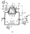
- a thermionic cathode 3 is mounted insulated in a cathode chamber 1. Areas 17 of the cathode chamber 1 surround an aperture 9.
- the cathode chamber 1 is mounted on the wall of the treatment chamber 11 via insulation supports 22. It encloses a screen 20, which is operated in a floating manner both with respect to the cathode chamber 1 and with respect to the treatment chamber 11, the parts 17 at a dark space distance d up to directly into the area of the aperture 9.
- the thermionic cathode is operated by means of a source 24 with the heating current I H and is led via a voltage source 26 and, generally speaking, a unit 28 to at least part of the cathode chamber wall, preferably to the cathode chamber wall itself.
- the unit 28 acts as a current limiter and, as a function of the current i flowing through it, causes a voltage drop and.
- it can be implemented by a current-controlled voltage source, but is preferably implemented by a passive switching element, in particular by a resistance element 30.
- the positive pole of the voltage source 26 can be at a reference potential, be it mass, or another predetermined potential laid or can be operated potential-free, like this purely schematically through the possibility switch 32 is shown.
- the treatment chamber 11 because of the cathode chamber 1 electrically insulated, the treatment chamber 11, as shown purely schematically with the possibility switch 34, to ground potential, to a reference potential or possibly even operated floating.
- the Treatment chamber inner wall 36 or at least lots thereof can be connected with respect to the thermionic cathode 3 as an anode his; but preferably a separate anode 38, as shown in dashed lines, provided which over a Voltage source 40 with respect to the thermionic cathode 3 anodic, i.e. positive, is wired.
- the anode 38 will preferably as a workpiece carrier for the schematically entered workpieces W used.
- the cathode chamber becomes a working gas, for example, via gas feed line 41 and preferably argon.
- gas feed line 41 Over a further, schematically illustrated gas feed line 43, such as shown schematically with the possibility switch 35, each after the potential of the chamber 11 can be placed on potential the hydrogen-containing gas G, preferably hydrogen, fed.
- the gas G is represented by a schematically Valve 52 inserted.
- a pump arrangement 42 is provided in order to pump out the chamber 11 and optionally the cathode chamber 1, wherein, as shown, a pump arrangement 42a can additionally be provided in order to pump out the cathode chamber separately.
- the diaphragm arrangement with the diaphragm opening 9 acts as a pressure stage between the pressure in the cathode chamber 1 and the pressure in the treatment chamber 11.
- the dilution gas for example N 2 , can be fed to the pump arrangement 42. This enables a nitrogen flow to be generated which reduces or dilutes the hydrogen to less than 4% by volume in the gas so that the gas can be released into the environment without hesitation. There is no longer any ignitable, explosive gas.
- the partial pressure of the hydrogen-containing gas G can be kept significantly higher in the treatment chamber 11 than in the cathode chamber 1, which makes it possible to significantly increase the service life of the thermionic cathode 3.
- the working pressure was: approx. 6 ⁇ 10 -3 mbar.
- the lead frame surface that comes with the packaging material in Contact stand (b) is due to its high level of contamination practically unsolderable.
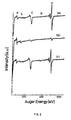
- Auger diagrams are untreated on the one hand, treated and subsequently exposed to air On the other hand, hardly distinguish surfaces.
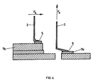
- the test stresses for wire bonding are defined in FIG. 4.
- the load F S of a thin wire 3, the surface of which is connected at a connection point 5 to the surface of a lead frame 7a or chip 7b, is referred to as shear load, while the load Fp is referred to as tensile load.
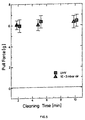
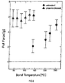
- the bond quality is that treated according to the invention Surfaces largely independent of temperature, what the effort required to control the temperature when bonding reduced. That low bond temperatures according to the invention can be used is particularly important, for example for "Ball Grid" arrays HLST made of organic material, which are bonded at low temperatures ⁇ 150 ° C have to.
- the bond temperatures that can be used according to the invention in FIG. 6 are much lower than the bond temperatures that are common be used. It can only be assumed today that the treatment according to the invention preservation thereby causing the metal surface to become hydrogen is saturated, there is contamination on the surface separate and practically float on the hydrogen cover, so their characteristic in the Auger diagram - in that Hydrogen not proven or only indirectly and with difficulty can be practically as unpurified after exposure to air appears, but how high for bonding or connecting qualitatively cleaned. When supplying the connection energy, e.g. Ultrasound during bonding, the hydrogen bonds are conserving obviously slightly broken open and the bare metal surface exposed for connection.
- connection energy e.g. Ultrasound during bonding
- FIGS. 5, 6 characterize those according to the invention Surface pairs versus pairs according to FIG. 3 (a) and their poor connectivity according to FIG. 6.
- Uncleaned HLST showed tensile load values of the bonded Wires less than 5cN, while according to the invention surface-treated values of over 6cN were observed. In most cases the wire broke before it broke the liaison office came.
Landscapes
- Physics & Mathematics (AREA)
- Engineering & Computer Science (AREA)
- Plasma & Fusion (AREA)
- Chemical & Material Sciences (AREA)
- Analytical Chemistry (AREA)
- Optics & Photonics (AREA)
- Mechanical Engineering (AREA)
- Wire Bonding (AREA)
- Cleaning In General (AREA)
- Adhesives Or Adhesive Processes (AREA)
- Pressure Welding/Diffusion-Bonding (AREA)
Description
Dieser Schritt ist als Wire Bonding (Draht-Bonden) bekannt.
- Research disclosure 307 107, worin, im Zusammenhang mit einem Härtungsverfahren, eine harte Schicht durch Elektronenstrahl-Oberflächenbeaufschlagung erzeugt wird;
- GB-2 131 619, wonach mechanisch belastete elektrische Kontaktflächen von Schaltkontakten zur Reinigung einer Plasmaentladung, vorzugsweise einer Hf-Plasmaentladung, in einer wasserstoff-, sauerstoff-, schwefelhexafluoridetc. enthaltenden Atmosphäre gereinigt werden;
- S. Veprek et al., "Recent Progress in the Restoration of Archeological Metallic Artifacts by Means of Low-Pressure Plasma Treatment", aus: Plasma Chemistry and Plasma Processing, Vol. 8, No. 4, 1988, wonach Oberflächen archäologischer metallischer Funde in einer Plasmaentladung in wasserstoffenthaltender Atmosphäre konserviert werden;
- K. Pickering et al., "Hydrogen plasmas for flux free flip-chip solder bonding", aus: J.Vac.Sci.Technol. A8(3), May/June 1990, American Vacuum Society, wonach Pb-Sn-Löten in einem Mikrowellenplasma in Wasserstoff enthaltender Atmosphäre vorgenommen wird;
- V. Zhukov et al., "Coadsorption of hydrogen and potassium on silver single crystal surfaces", aus: Pergamon, Vacuum/volume 47/number 1, 1995, Elsevier Science Ltd., wonach festgestellt wurde, dass, durch Wasserstoffadsorption, Edelmetall-Oberflächen passiviert werden;
- N. Koopman et al., "Fluxless Soldering in Air and Nitrogen", aus: I.N., 1993 Proceedings, 43rd Electronic Components and Technology Conference (Cat.No. 93CH3205/2), Proceedings of IEEE, 43rd Electronic Components and Technology Conference (ECTC'93), Orlando, 1st to 4th June 1993, woraus es bekannt ist, Oxide an einer Lotoberfläche in Oxifluoride zu wandeln. Damit werde eine hohe Passivierung gegenüber Luft erreicht, so dass so behandelte Oberflächen bis zu einer Woche an Luft gelagert werden könnten, vor reflow-Verbindung.
- Fig. 1
- schematisch, den Aufbau einer erfindungsgemässen Anlage, wie sie für die beschriebenen Versuche eingesetzt wurde;
- Fig. 2
- die Auger-Spektren zweier lead frame-Oberflächen von Weichlotsubstraten, welche aus derselben Verpackungseinheit stammen und darin unterschiedliche Abstände zum Verpackungsmaterial hatten;
- Fig. 3
- die Auger-Spektren von Oberflächen für die Erstellung einer Weichlotverbindung, unvorbehandelt (a), erfindungsgemäss vorbehandelt (b) sowie erfindungsgemäss vorbehandelt und darnach Luft ausgesetzt (c);
- Fig. 4
- schematisch, die Definition der Scherungsbelastung und der Zugbelastung von wire-bond-Verbindungsstellen;
- Fig. 5
- in Funktion der Behandlungszeit zu verbindender erfindungsgemässer Oberflächen für wire bonding sowie des Druckes bei der erfindungsgemässen Oberflächenbehandlung, die Zugbelastbarkeit erfindungsgemäss behandelter, luftgelagerter und anschliessend Ultraschall-wire-gebondeter Oberflächen von QFP (Quad Flat Pack) Cu lead frames mit versilberten leads (Kontakten);
- Fig. 6
- in Abhängigkeit der Bond-Temperatur, die Zugbelastbarkeit Ultraschall-gebondeter, unvorbehandelter sowie erfindungsgemäss vorbehandelter und gelagerter Oberflächen.
- DE-OS-43 10 941, entsprechend der US-5 384 018;
- der DE-40 29 270, entsprechend der EP-478 909 bzw. der DE-4 029 268 entsprechend der US-5 336 326;
- der EP-510 340, entsprechend der US-5 308 950.
- metallische lead frames für Weichloten, beispielsweise aus Cu, vernickeltem Cu, silberplattiertem Cu,
- organische HLST-Materialien, wie BGA (ball grid arrays) und MCM (multi chip modules), beispielsweise auf Epoxy- oder Esterbasis, sowie PCB (printed chip boards),
- metallische QFP (quad flat packe), beispielsweise aus Cu, versilbertem CU, Pd-plattiertem Cu,
- die Metallisierung der Leiterbahnen für die organischen HLST-Materialien und die QFP, beispielsweise aus versilbertem Cu, vergoldetem Cu, Au,
- Halbleitersubstratträger als Flip Chip ausgebildet mit Lötpunkten, beispielsweise aus AgSn, PbSn, PbSnAg, PbInAg,
- HLST-Materialien auf Keramikbasis, beispielsweise Aluminiumoxid,
- Oberflächenschutzschicht der Chips, beispielsweise aus Siliziumnitrid, Siliziumoxinitrid, Polyimid,
Einschalten der Gasflüsse:
- Argon durch Leitung 41,
Fluss FlAr : 10sccm ≤ FlAr ≤ 50sccm, - Wasserstoff durch Leitung 43,
Fluss FlH2 : 10sccm ≤ FlH2 ≤ 50sccm.
- (a) einer unbehandelten lead frame-Kupferoberfläche für Weichlotverbindung nach Kontaktierung mit einem Verpackungsmaterial;
- (b) einer solchen Oberfläche innerhalb derselben Verpackungseinheit, aber nicht in Kontakt mit dem Verpackungsmaterial.
- (a) unbehandelter lead-frame-Oberflächen für Weichlotverbindung,
- (b) solcher nach oben beschriebenen Vorgehen behandelten Oberflächen unmittelbar nach deren Behandlung und
- (c) solcher Oberflächen nach Kurve (b), aber nach deren Lagerung während ca. 1h und mehr in Luft.
Claims (21)
- Verfahren zur Herstellung von Werkstücken, bei dem Oberflächen von Teilen Luft ausgesetzt werden und danach ohne weitere zusätzliche Behandlung gebondet, geklebt oder vergossen werden und sie hierfür vor dem Luftaussetzen einer Atmosphäre mit aktiviertem Wasserstoff ausgesetzt werden.
- Verfahren nach Anspruch 1, dadurch gekennzeichnet, dass man den Wasserstoff der Atmosphäre mittels einer Plasmaentladung oder mittels Licht, insbesondere mittels UV-Strahlung, aktiviert.
- Verfahren nach einem der Ansprüche 1 oder 2, bei dem die Oberflächen metallisch, halbmetallisch oder aus Kunststoff sind, bevorzugterweise metallisch.
- Verfahren nach einem der Ansprüche 1 bis 3, dadurch gekennzeichnet, dass man den Wasserstoff mittels einer Niederspannungsentladung anregt.
- Verfahren nach Anspruch 4, dadurch gekennzeichnet, dass man die Niederspannungsentladung mittels einer thermionischen Kathode betreibt.
- Verfahren nach einem der Ansprüche 1 bis 5, dadurch gekennzeichnet, dass man als Atmosphäre eine Vakuumatmosphäre wählt.
- Verfahren nach einem der Ansprüche 1 bis 6, dadurch gekennzeichnet, dass man in der Atmosphäre eine Plasmaentladung unterhält und die Atmosphäre ein Arbeitsgas enthält, vorzugsweise Argon.
- Verfahren nach einem der Ansprüche 1 bis 7, dadurch gekennzeichnet, dass man den Wasserstoff mittels einer Plasmaentladung aktiviert in einer ausschliesslich Wasserstoff und ein Arbeitsgas für die Entladung enthaltenden Atmosphäre.
- Verfahren nach einem der Ansprüche 1 bis 8, dadurch gekennzeichnet, dass man den Wasserstoff mittels einer Plasmaentladung anregt, deren Entladespannung kleiner als 30V ist und die einen Entladestrom vorzugsweise zwischen 10A und 100A aufweist.
- Verfahren nach einem der Ansprüche 1 bis 9, dadurch gekennzeichnet, dass die Oberflächen ultraschallverschweisst werden.
- Verfahren nach einem der Ansprüche 1 bis 10, dadurch gekennzeichnet, dass man die Oberfläche mindestens eines der Halbfabrikate auf höchstens 150°C erhitzt.
- Verwendung des Verfahrens nach einem der Ansprüche 1 bis 11 für die Herstellung von Werkstücken durch Verbinden integrierter Schaltkreis mit einem HLST oder durch elektrisches Kontaktieren integrierter Schaltkreise durch Wire Bonding oder durch Umhüllen von mit HLST verbundenen, durch Wire Bonding kontaktierten, elektrischen Schaltkreisen mit einer Gussmasse.
- Verwendung des Verfahrens nach einem der Ansprüche 1 bis 11 für Flip Chip zu verbindende und zu positionierende integrierte Schaltkreise und HLST, durch Aufschmelzen von Lötpunkten von Schaltkreis und HLST.
- Verwendung einer Behandlung von Teilen, bei der die Teile einer Atmosphäre mit aktiviertem Wasserstoff ausgesetzt werden, für das Erreichen einer Bond-, Kleb- oder Vergiessbarkeit der Teile ohne zusätzliche Behandlung, nachdem die Teile, nach der Wasserstoffbehandlung, Luft ausgesetzt sind.
- Verwendung nach Anspruch 14, dadurch gekennzeichnet, dass die Oberfläche metallisch, halbmetallisch oder eine Kunststoff-Oberfläche ist, insbesondere eine metallische.
- Verwendung nach einem der Ansprüche 14 oder 15, dadurch gekennzeichnet, dass man die Entladung in einer Arbeitsgas enthaltenden Atmosphäre unterhält, vorzugsweise in einer Argon enthaltenden.
- Verwendung nach Anspruch 16, dadurch gekennzeichnet, dass die Atmosphäre ausschliesslich Wasserstoff und das Arbeitsgas enthält.
- Verwendung nach einem der Ansprüche 14 bis 17, dadurch gekennzeichnet, dass die Entladespannung kleiner als 30 V ist und die Entladung einen Entladestrom vorzugsweise zwischen 10 A und 100 A hat.
- Verwendung nach einem der Ansprüche 14 bis 18, dadurch gekennzeichnet, dass die ultraschallverschweisst werden können.
- Verwendung nach einem der Ansprüche 14 bis 19, dadurch gekennzeichnet, dass die Teile höchstens auf 150°C erhitzt werden dürfen.
- Verwendung des Verfahren nach einem der Ansprüche 14 bis 20 für integrierte Schaltkreise oder HLST.
Applications Claiming Priority (4)
| Application Number | Priority Date | Filing Date | Title |
|---|---|---|---|
| CH00948/96A CH692446A5 (de) | 1996-04-15 | 1996-04-15 | Verfahren zur Herstellung von Werkstücken und von Teilen hierfür |
| CH948/96 | 1996-04-15 | ||
| CH94896 | 1996-04-15 | ||
| PCT/CH1997/000147 WO1997039472A1 (de) | 1996-04-15 | 1997-04-14 | Verwendung eines reinigungsverfahrens, reinigungsverfahren, verbindungsverfahren und werkstückpaar |
Publications (3)
| Publication Number | Publication Date |
|---|---|
| EP0894332A1 EP0894332A1 (de) | 1999-02-03 |
| EP0894332B1 true EP0894332B1 (de) | 2003-05-21 |
| EP0894332B8 EP0894332B8 (de) | 2003-12-17 |
Family
ID=4198897
Family Applications (1)
| Application Number | Title | Priority Date | Filing Date |
|---|---|---|---|
| EP97915247A Expired - Lifetime EP0894332B8 (de) | 1996-04-15 | 1997-04-14 | Verwendung verbindungsverfahrens und verbindungsverfahren |
Country Status (6)
| Country | Link |
|---|---|
| US (3) | US6203637B1 (de) |
| EP (1) | EP0894332B8 (de) |
| JP (1) | JP4086902B2 (de) |
| CH (1) | CH692446A5 (de) |
| DE (1) | DE59710130D1 (de) |
| WO (1) | WO1997039472A1 (de) |
Families Citing this family (22)
| Publication number | Priority date | Publication date | Assignee | Title |
|---|---|---|---|---|
| CH692446A5 (de) * | 1996-04-15 | 2002-06-28 | Esec Sa | Verfahren zur Herstellung von Werkstücken und von Teilen hierfür |
| FR2778190B1 (fr) * | 1998-05-04 | 2000-06-02 | Air Liquide | Procede et appareil de traitement de surfaces metalliques par voie seche |
| US6605175B1 (en) | 1999-02-19 | 2003-08-12 | Unaxis Balzers Aktiengesellschaft | Process for manufacturing component parts, use of same, with air bearing supported workpieces and vacuum processing chamber |
| US6749691B2 (en) | 2001-02-14 | 2004-06-15 | Air Liquide America, L.P. | Methods of cleaning discolored metallic arrays using chemical compositions |
| US6776330B2 (en) * | 2001-09-10 | 2004-08-17 | Air Products And Chemicals, Inc. | Hydrogen fluxless soldering by electron attachment |
| US6902774B2 (en) | 2002-07-25 | 2005-06-07 | Inficon Gmbh | Method of manufacturing a device |
| US7387738B2 (en) | 2003-04-28 | 2008-06-17 | Air Products And Chemicals, Inc. | Removal of surface oxides by electron attachment for wafer bumping applications |
| US7079370B2 (en) * | 2003-04-28 | 2006-07-18 | Air Products And Chemicals, Inc. | Apparatus and method for removal of surface oxides via fluxless technique electron attachment and remote ion generation |
| US7897029B2 (en) * | 2008-03-04 | 2011-03-01 | Air Products And Chemicals, Inc. | Removal of surface oxides by electron attachment |
| US8361340B2 (en) | 2003-04-28 | 2013-01-29 | Air Products And Chemicals, Inc. | Removal of surface oxides by electron attachment |
| US6980015B2 (en) * | 2003-06-17 | 2005-12-27 | Agilent Technologies, Inc. | Back side probing method and assembly |
| KR20130019006A (ko) * | 2005-05-04 | 2013-02-25 | 오를리콘 트레이딩 아크티엔게젤샤프트, 트뤼프바흐 | 플라즈마 처리 장치용 플라즈마 증폭기 |
| US7434719B2 (en) * | 2005-12-09 | 2008-10-14 | Air Products And Chemicals, Inc. | Addition of D2 to H2 to detect and calibrate atomic hydrogen formed by dissociative electron attachment |
| US20070243713A1 (en) * | 2006-04-12 | 2007-10-18 | Lam Research Corporation | Apparatus and method for generating activated hydrogen for plasma stripping |
| KR101046520B1 (ko) | 2007-09-07 | 2011-07-04 | 어플라이드 머티어리얼스, 인코포레이티드 | 내부 챔버 상의 부산물 막 증착을 제어하기 위한 pecvd 시스템에서의 소스 가스 흐름 경로 제어 |
| US8454850B2 (en) | 2009-09-02 | 2013-06-04 | Air Products And Chemicals, Inc. | Method for the removal of surface oxides by electron attachment |
| US9006975B2 (en) | 2011-02-09 | 2015-04-14 | Air Products And Chemicals, Inc. | Apparatus and method for removal of surface oxides via fluxless technique involving electron attachment |
| US9053894B2 (en) | 2011-02-09 | 2015-06-09 | Air Products And Chemicals, Inc. | Apparatus and method for removal of surface oxides via fluxless technique involving electron attachment |
| JP6219227B2 (ja) * | 2014-05-12 | 2017-10-25 | 東京エレクトロン株式会社 | ヒータ給電機構及びステージの温度制御方法 |
| JP7890698B2 (ja) * | 2022-06-22 | 2026-07-15 | 住友電気工業株式会社 | 接合装置および接合方法 |
| CN115430663A (zh) * | 2022-08-17 | 2022-12-06 | 成都飞机工业(集团)有限责任公司 | 一种电子束金属表面清洗方法 |
| CN117798451B (zh) * | 2024-03-01 | 2024-04-30 | 深圳市志胜威电子设备有限公司 | 一种选择性波峰焊喷锡装置 |
Family Cites Families (10)
| Publication number | Priority date | Publication date | Assignee | Title |
|---|---|---|---|---|
| JP2663580B2 (ja) * | 1988-11-22 | 1997-10-15 | 日本電気株式会社 | シリコン表面のパッシベーション方法及び装置 |
| GB8827933D0 (en) * | 1988-11-30 | 1989-01-05 | Plessey Co Plc | Improvements relating to soldering processes |
| DE4032328A1 (de) * | 1989-11-06 | 1991-09-19 | Wls Karl Heinz Grasmann Weichl | Verfahren und vorrichtung zur verarbeitung von zu verloetenden fuegepartnern |
| DE4029268C2 (de) | 1990-09-14 | 1995-07-06 | Balzers Hochvakuum | Verfahren zur gleichspannungs-bogenentladungs-unterstützten, reaktiven Behandlung von Gut und Vakuumbehandlungsanlage zur Durchführung |
| DE4029270C1 (de) | 1990-09-14 | 1992-04-09 | Balzers Ag, Balzers, Li | |
| DE59202116D1 (de) | 1991-04-23 | 1995-06-14 | Balzers Hochvakuum | Verfahren zur Abtragung von Material von einer Oberfläche in einer Vakuumkammer. |
| US5376223A (en) * | 1992-01-09 | 1994-12-27 | Varian Associates, Inc. | Plasma etch process |
| CH687111A5 (de) * | 1992-05-26 | 1996-09-13 | Balzers Hochvakuum | Verfahren zum Erzeugen einer Niederspannungsentladung, Vakuumbehandlungsanlage hierfuer sowie Anwendung des Verfahrens. |
| US5409543A (en) * | 1992-12-22 | 1995-04-25 | Sandia Corporation | Dry soldering with hot filament produced atomic hydrogen |
| CH692446A5 (de) * | 1996-04-15 | 2002-06-28 | Esec Sa | Verfahren zur Herstellung von Werkstücken und von Teilen hierfür |
-
1996
- 1996-04-15 CH CH00948/96A patent/CH692446A5/de not_active IP Right Cessation
-
1997
- 1997-04-14 EP EP97915247A patent/EP0894332B8/de not_active Expired - Lifetime
- 1997-04-14 JP JP53661897A patent/JP4086902B2/ja not_active Expired - Fee Related
- 1997-04-14 WO PCT/CH1997/000147 patent/WO1997039472A1/de not_active Ceased
- 1997-04-14 DE DE59710130T patent/DE59710130D1/de not_active Expired - Lifetime
-
1998
- 1998-10-15 US US09/172,598 patent/US6203637B1/en not_active Expired - Lifetime
-
2000
- 2000-12-05 US US09/729,176 patent/US6503351B2/en not_active Expired - Fee Related
-
2002
- 2002-10-16 US US10/270,495 patent/US20030051792A1/en not_active Abandoned
Also Published As
| Publication number | Publication date |
|---|---|
| US20030051792A1 (en) | 2003-03-20 |
| US20010001184A1 (en) | 2001-05-17 |
| EP0894332B8 (de) | 2003-12-17 |
| EP0894332A1 (de) | 1999-02-03 |
| US6203637B1 (en) | 2001-03-20 |
| JP2001505119A (ja) | 2001-04-17 |
| CH692446A5 (de) | 2002-06-28 |
| US6503351B2 (en) | 2003-01-07 |
| JP4086902B2 (ja) | 2008-05-14 |
| WO1997039472A1 (de) | 1997-10-23 |
| DE59710130D1 (de) | 2003-06-26 |
Similar Documents
| Publication | Publication Date | Title |
|---|---|---|
| CH692446A5 (de) | Verfahren zur Herstellung von Werkstücken und von Teilen hierfür | |
| US6902774B2 (en) | Method of manufacturing a device | |
| WO2000048779A1 (de) | Verfahren zur herstellung von bauteilen, verwendung desselben, luftgelagertes werkstück und vakuumbehandlungskammer | |
| DE60210858T2 (de) | Elektronische Vorrichtung mit einem Al- oder Co-Teilchen enthaltenden Lot aus einer Zn-Al-Ge-Mg Legierung | |
| US4921157A (en) | Fluxless soldering process | |
| US8567658B2 (en) | Method of plasma preparation of metallic contacts to enhance mechanical and electrical integrity of subsequent interconnect bonds | |
| US6935553B2 (en) | Reflow soldering method | |
| KR20080071984A (ko) | 수지 비함유성 용제가 포함된 납땜용 페이스트 | |
| EP2487002A1 (de) | Vorrichtung und Verfahren zum Entfernen von Oberflächenoxiden über flussmittelfreie Technik mit Elektronenanlagerung | |
| DE19546569C2 (de) | Lötverbindungsverfahren und Verwendung dieses Verfahrens zur Herstellung eines Leistungshalbleiters | |
| US5776551A (en) | Use of plasma activated NF3 to clean solder bumps on a device | |
| DE102013200868B4 (de) | Verfahren zur Herstellung einer stoffschlüssigen Verbindung und einer elektrischen Verbindung | |
| DE2518305A1 (de) | Verfahren zum anbringen eines leiterteils an einer halbleitereinrichtung und eine nach diesem verfahren hergestellte halbleitereinrichtung | |
| JP2006167735A (ja) | 機器、構造材等の製造法 | |
| KR100512521B1 (ko) | 세정방법의사용방법,세정방법,결합방법및공작재료쌍 | |
| EP1865760B1 (de) | Lötverfahren | |
| WO1996030939A1 (de) | Verfahren zur flächenkontaktierung elektronischer bauelemente | |
| DE19654250A1 (de) | Verfahren und Vorrichtung zum Herstellen oxidationsempfindlicher Lötverbindunden | |
| DE10203112A1 (de) | Verfahren zur Verbesserung der Qualität von Lötverbindungen | |
| DE19738118A1 (de) | Montageverfahren für ein Halbleiterbauelement | |
| DE68922949T2 (de) | Verfahren zum Schmelzbeschichten in einer Atmosphäre mit gesteuerter Oxydationsfähigkeit. | |
| EP2022591B1 (de) | Verfahren zur Erzeugung einer lötfähigen metallischen Oberfläche und Lötverfahren | |
| DE102012207560B4 (de) | Verfahren zur herstellung und zum betrieb eines halbleitermoduls | |
| DE10312109A1 (de) | Herstellung von Lotkontakten auf einem Wafer unter Verwendung einer strukturierten Lotfolie | |
| EP1330327A1 (de) | Verfahren zum flussmittelfreien aufbringen eines lötmittels auf ein substrat oder einen chip |
Legal Events
| Date | Code | Title | Description |
|---|---|---|---|
| PUAI | Public reference made under article 153(3) epc to a published international application that has entered the european phase |
Free format text: ORIGINAL CODE: 0009012 |
|
| 17P | Request for examination filed |
Effective date: 19980905 |
|
| AK | Designated contracting states |
Kind code of ref document: A1 Designated state(s): DE FR GB IE IT |
|
| 17Q | First examination report despatched |
Effective date: 19990730 |
|
| RAP1 | Party data changed (applicant data changed or rights of an application transferred) |
Owner name: ESEC SA Owner name: UNAXIS BALZERS AKTIENGESELLSCHAFT |
|
| RTI1 | Title (correction) |
Free format text: USE OF A CONNECTING PROCESS AND CONNECTING PROCESS |
|
| GRAH | Despatch of communication of intention to grant a patent |
Free format text: ORIGINAL CODE: EPIDOS IGRA |
|
| GRAH | Despatch of communication of intention to grant a patent |
Free format text: ORIGINAL CODE: EPIDOS IGRA |
|
| GRAH | Despatch of communication of intention to grant a patent |
Free format text: ORIGINAL CODE: EPIDOS IGRA |
|
| GRAA | (expected) grant |
Free format text: ORIGINAL CODE: 0009210 |
|
| AK | Designated contracting states |
Designated state(s): DE FR GB IE IT |
|
| REG | Reference to a national code |
Ref country code: GB Ref legal event code: FG4D Free format text: NOT ENGLISH |
|
| REG | Reference to a national code |
Ref country code: IE Ref legal event code: FG4D Free format text: GERMAN |
|
| REF | Corresponds to: |
Ref document number: 59710130 Country of ref document: DE Date of ref document: 20030626 Kind code of ref document: P |
|
| RBV | Designated contracting states (corrected) |
Designated state(s): DE FR GB IE IT NL |
|
| GBT | Gb: translation of ep patent filed (gb section 77(6)(a)/1977) | ||
| ET | Fr: translation filed | ||
| PLBE | No opposition filed within time limit |
Free format text: ORIGINAL CODE: 0009261 |
|
| STAA | Information on the status of an ep patent application or granted ep patent |
Free format text: STATUS: NO OPPOSITION FILED WITHIN TIME LIMIT |
|
| 26N | No opposition filed |
Effective date: 20040224 |
|
| PGFP | Annual fee paid to national office [announced via postgrant information from national office to epo] |
Ref country code: NL Payment date: 20050403 Year of fee payment: 9 |
|
| PGFP | Annual fee paid to national office [announced via postgrant information from national office to epo] |
Ref country code: IE Payment date: 20050414 Year of fee payment: 9 |
|
| PG25 | Lapsed in a contracting state [announced via postgrant information from national office to epo] |
Ref country code: IE Free format text: LAPSE BECAUSE OF NON-PAYMENT OF DUE FEES Effective date: 20060414 |
|
| PG25 | Lapsed in a contracting state [announced via postgrant information from national office to epo] |
Ref country code: NL Free format text: LAPSE BECAUSE OF NON-PAYMENT OF DUE FEES Effective date: 20061101 |
|
| NLV4 | Nl: lapsed or anulled due to non-payment of the annual fee |
Effective date: 20061101 |
|
| REG | Reference to a national code |
Ref country code: IE Ref legal event code: MM4A |
|
| PGFP | Annual fee paid to national office [announced via postgrant information from national office to epo] |
Ref country code: GB Payment date: 20100325 Year of fee payment: 14 |
|
| PGFP | Annual fee paid to national office [announced via postgrant information from national office to epo] |
Ref country code: FR Payment date: 20100521 Year of fee payment: 14 |
|
| PGFP | Annual fee paid to national office [announced via postgrant information from national office to epo] |
Ref country code: DE Payment date: 20100430 Year of fee payment: 14 |
|
| PG25 | Lapsed in a contracting state [announced via postgrant information from national office to epo] |
Ref country code: IT Free format text: LAPSE BECAUSE OF NON-PAYMENT OF DUE FEES Effective date: 20090414 |
|
| PGFP | Annual fee paid to national office [announced via postgrant information from national office to epo] |
Ref country code: IT Payment date: 20090424 Year of fee payment: 13 |
|
| PGRI | Patent reinstated in contracting state [announced from national office to epo] |
Ref country code: IT Effective date: 20110616 |
|
| REG | Reference to a national code |
Ref country code: DE Ref legal event code: R119 Ref document number: 59710130 Country of ref document: DE |
|
| REG | Reference to a national code |
Ref country code: DE Ref legal event code: R119 Ref document number: 59710130 Country of ref document: DE |
|
| GBPC | Gb: european patent ceased through non-payment of renewal fee |
Effective date: 20110414 |
|
| REG | Reference to a national code |
Ref country code: FR Ref legal event code: ST Effective date: 20111230 |
|
| PG25 | Lapsed in a contracting state [announced via postgrant information from national office to epo] |
Ref country code: FR Free format text: LAPSE BECAUSE OF NON-PAYMENT OF DUE FEES Effective date: 20110502 |
|
| PG25 | Lapsed in a contracting state [announced via postgrant information from national office to epo] |
Ref country code: GB Free format text: LAPSE BECAUSE OF NON-PAYMENT OF DUE FEES Effective date: 20110414 |
|
| PG25 | Lapsed in a contracting state [announced via postgrant information from national office to epo] |
Ref country code: DE Free format text: LAPSE BECAUSE OF NON-PAYMENT OF DUE FEES Effective date: 20111031 |
|
| PGRI | Patent reinstated in contracting state [announced from national office to epo] |
Ref country code: IT Effective date: 20110616 |