EP0893794B1 - Optical recording media and recording thereon - Google Patents
Optical recording media and recording thereon Download PDFInfo
- Publication number
- EP0893794B1 EP0893794B1 EP98305833A EP98305833A EP0893794B1 EP 0893794 B1 EP0893794 B1 EP 0893794B1 EP 98305833 A EP98305833 A EP 98305833A EP 98305833 A EP98305833 A EP 98305833A EP 0893794 B1 EP0893794 B1 EP 0893794B1
- Authority
- EP
- European Patent Office
- Prior art keywords
- data
- recording
- disk
- track
- address
- Prior art date
- Legal status (The legal status is an assumption and is not a legal conclusion. Google has not performed a legal analysis and makes no representation as to the accuracy of the status listed.)
- Expired - Lifetime
Links
- 230000003287 optical effect Effects 0.000 title claims abstract description 68
- 238000000034 method Methods 0.000 abstract description 49
- 230000008569 process Effects 0.000 abstract description 30
- 230000002093 peripheral effect Effects 0.000 abstract description 12
- 239000011295 pitch Substances 0.000 description 37
- 238000001514 detection method Methods 0.000 description 34
- 238000010586 diagram Methods 0.000 description 32
- 238000005520 cutting process Methods 0.000 description 19
- 239000000758 substrate Substances 0.000 description 14
- 239000011521 glass Substances 0.000 description 12
- 238000013316 zoning Methods 0.000 description 12
- 230000006870 function Effects 0.000 description 10
- 239000000969 carrier Substances 0.000 description 8
- 239000010410 layer Substances 0.000 description 8
- 238000012937 correction Methods 0.000 description 7
- 230000002194 synthesizing effect Effects 0.000 description 7
- 230000004044 response Effects 0.000 description 6
- 230000008859 change Effects 0.000 description 5
- 230000000694 effects Effects 0.000 description 5
- 238000004519 manufacturing process Methods 0.000 description 5
- 229920002120 photoresistant polymer Polymers 0.000 description 5
- 238000012360 testing method Methods 0.000 description 5
- 238000004364 calculation method Methods 0.000 description 3
- 238000012545 processing Methods 0.000 description 3
- IUQJDHJVPLLKFL-UHFFFAOYSA-N 2-(2,4-dichlorophenoxy)acetate;dimethylazanium Chemical compound CNC.OC(=O)COC1=CC=C(Cl)C=C1Cl IUQJDHJVPLLKFL-UHFFFAOYSA-N 0.000 description 2
- 230000007547 defect Effects 0.000 description 2
- 239000002184 metal Substances 0.000 description 2
- 230000000704 physical effect Effects 0.000 description 2
- 230000010076 replication Effects 0.000 description 2
- 238000005452 bending Methods 0.000 description 1
- 230000008901 benefit Effects 0.000 description 1
- 238000006243 chemical reaction Methods 0.000 description 1
- 239000011248 coating agent Substances 0.000 description 1
- 238000000576 coating method Methods 0.000 description 1
- 230000002950 deficient Effects 0.000 description 1
- 230000001419 dependent effect Effects 0.000 description 1
- 230000006866 deterioration Effects 0.000 description 1
- 238000011161 development Methods 0.000 description 1
- 239000002355 dual-layer Substances 0.000 description 1
- 238000002347 injection Methods 0.000 description 1
- 239000007924 injection Substances 0.000 description 1
- 238000003780 insertion Methods 0.000 description 1
- 230000037431 insertion Effects 0.000 description 1
- 238000007689 inspection Methods 0.000 description 1
- 230000001678 irradiating effect Effects 0.000 description 1
- 238000010030 laminating Methods 0.000 description 1
- 238000007726 management method Methods 0.000 description 1
- 238000005259 measurement Methods 0.000 description 1
- 238000012986 modification Methods 0.000 description 1
- 230000004048 modification Effects 0.000 description 1
- 239000011347 resin Substances 0.000 description 1
- 229920005989 resin Polymers 0.000 description 1
- 230000035945 sensitivity Effects 0.000 description 1
- 239000002356 single layer Substances 0.000 description 1
- 230000001360 synchronised effect Effects 0.000 description 1
- 238000012546 transfer Methods 0.000 description 1
Images


Classifications
-
- G—PHYSICS
- G11—INFORMATION STORAGE
- G11B—INFORMATION STORAGE BASED ON RELATIVE MOVEMENT BETWEEN RECORD CARRIER AND TRANSDUCER
- G11B7/00—Recording or reproducing by optical means, e.g. recording using a thermal beam of optical radiation by modifying optical properties or the physical structure, reproducing using an optical beam at lower power by sensing optical properties; Record carriers therefor
- G11B7/24—Record carriers characterised by shape, structure or physical properties, or by the selection of the material
- G11B7/2407—Tracks or pits; Shape, structure or physical properties thereof
- G11B7/24073—Tracks
- G11B7/24082—Meandering
-
- G—PHYSICS
- G11—INFORMATION STORAGE
- G11B—INFORMATION STORAGE BASED ON RELATIVE MOVEMENT BETWEEN RECORD CARRIER AND TRANSDUCER
- G11B20/00—Signal processing not specific to the method of recording or reproducing; Circuits therefor
- G11B20/10—Digital recording or reproducing
- G11B20/12—Formatting, e.g. arrangement of data block or words on the record carriers
- G11B20/1217—Formatting, e.g. arrangement of data block or words on the record carriers on discs
-
- G—PHYSICS
- G11—INFORMATION STORAGE
- G11B—INFORMATION STORAGE BASED ON RELATIVE MOVEMENT BETWEEN RECORD CARRIER AND TRANSDUCER
- G11B7/00—Recording or reproducing by optical means, e.g. recording using a thermal beam of optical radiation by modifying optical properties or the physical structure, reproducing using an optical beam at lower power by sensing optical properties; Record carriers therefor
- G11B7/007—Arrangement of the information on the record carrier, e.g. form of tracks, actual track shape, e.g. wobbled, or cross-section, e.g. v-shaped; Sequential information structures, e.g. sectoring or header formats within a track
- G11B7/00736—Auxiliary data, e.g. lead-in, lead-out, Power Calibration Area [PCA], Burst Cutting Area [BCA], control information
-
- G—PHYSICS
- G11—INFORMATION STORAGE
- G11B—INFORMATION STORAGE BASED ON RELATIVE MOVEMENT BETWEEN RECORD CARRIER AND TRANSDUCER
- G11B7/00—Recording or reproducing by optical means, e.g. recording using a thermal beam of optical radiation by modifying optical properties or the physical structure, reproducing using an optical beam at lower power by sensing optical properties; Record carriers therefor
- G11B7/24—Record carriers characterised by shape, structure or physical properties, or by the selection of the material
- G11B7/2407—Tracks or pits; Shape, structure or physical properties thereof
- G11B7/24073—Tracks
- G11B7/24079—Width or depth
-
- G—PHYSICS
- G11—INFORMATION STORAGE
- G11B—INFORMATION STORAGE BASED ON RELATIVE MOVEMENT BETWEEN RECORD CARRIER AND TRANSDUCER
- G11B7/00—Recording or reproducing by optical means, e.g. recording using a thermal beam of optical radiation by modifying optical properties or the physical structure, reproducing using an optical beam at lower power by sensing optical properties; Record carriers therefor
- G11B7/24—Record carriers characterised by shape, structure or physical properties, or by the selection of the material
- G11B7/2407—Tracks or pits; Shape, structure or physical properties thereof
- G11B7/24085—Pits
-
- G—PHYSICS
- G11—INFORMATION STORAGE
- G11B—INFORMATION STORAGE BASED ON RELATIVE MOVEMENT BETWEEN RECORD CARRIER AND TRANSDUCER
- G11B20/00—Signal processing not specific to the method of recording or reproducing; Circuits therefor
- G11B20/10—Digital recording or reproducing
- G11B20/12—Formatting, e.g. arrangement of data block or words on the record carriers
- G11B20/1217—Formatting, e.g. arrangement of data block or words on the record carriers on discs
- G11B2020/1218—Formatting, e.g. arrangement of data block or words on the record carriers on discs wherein the formatting concerns a specific area of the disc
- G11B2020/1238—Formatting, e.g. arrangement of data block or words on the record carriers on discs wherein the formatting concerns a specific area of the disc track, i.e. the entire a spirally or concentrically arranged path on which the recording marks are located
- G11B2020/1239—Formatting, e.g. arrangement of data block or words on the record carriers on discs wherein the formatting concerns a specific area of the disc track, i.e. the entire a spirally or concentrically arranged path on which the recording marks are located the track being a pregroove, e.g. the wobbled track of a recordable optical disc
-
- G—PHYSICS
- G11—INFORMATION STORAGE
- G11B—INFORMATION STORAGE BASED ON RELATIVE MOVEMENT BETWEEN RECORD CARRIER AND TRANSDUCER
- G11B20/00—Signal processing not specific to the method of recording or reproducing; Circuits therefor
- G11B20/10—Digital recording or reproducing
- G11B20/12—Formatting, e.g. arrangement of data block or words on the record carriers
- G11B2020/1264—Formatting, e.g. arrangement of data block or words on the record carriers wherein the formatting concerns a specific kind of data
- G11B2020/1265—Control data, system data or management information, i.e. data used to access or process user data
- G11B2020/1267—Address data
- G11B2020/1268—Address in pregroove [ADIP] information
-
- G—PHYSICS
- G11—INFORMATION STORAGE
- G11B—INFORMATION STORAGE BASED ON RELATIVE MOVEMENT BETWEEN RECORD CARRIER AND TRANSDUCER
- G11B20/00—Signal processing not specific to the method of recording or reproducing; Circuits therefor
- G11B20/10—Digital recording or reproducing
- G11B20/12—Formatting, e.g. arrangement of data block or words on the record carriers
- G11B2020/1264—Formatting, e.g. arrangement of data block or words on the record carriers wherein the formatting concerns a specific kind of data
- G11B2020/1265—Control data, system data or management information, i.e. data used to access or process user data
- G11B2020/1277—Control data, system data or management information, i.e. data used to access or process user data for managing gaps between two recordings, e.g. control data in linking areas, run-in or run-out fields, guard or buffer zones
-
- G—PHYSICS
- G11—INFORMATION STORAGE
- G11B—INFORMATION STORAGE BASED ON RELATIVE MOVEMENT BETWEEN RECORD CARRIER AND TRANSDUCER
- G11B20/00—Signal processing not specific to the method of recording or reproducing; Circuits therefor
- G11B20/10—Digital recording or reproducing
- G11B20/12—Formatting, e.g. arrangement of data block or words on the record carriers
- G11B2020/1264—Formatting, e.g. arrangement of data block or words on the record carriers wherein the formatting concerns a specific kind of data
- G11B2020/1265—Control data, system data or management information, i.e. data used to access or process user data
- G11B2020/1278—Physical format specifications of the record carrier, e.g. compliance with a specific standard, recording density, number of layers, start of data zone or lead-out
Abstract
Description
- This invention relates to optical recording media, such as optical disks or the like. More particularly, but not exclusively, the invention relates to an optical disk on which address information is recorded by wobbling a track such as a pre-groove.
- To record data on a disk, address information must be recorded to enable data to be recorded at a predetermined position. The address information is sometimes recorded by wobbling.
- An example of a method to record the above-mentioned wobbling information on a track of a disk is disclosed in US Patent No. US-A-4 942 565.
- That is, a track on which data is recorded is in the form of a pre-groove which is previously formed. The side wall of the pre-groove is wobbled (allowed to meander) in response to the address information.
- Thus, the address can be read from the wobbling information. Therefore, even if bit data or the like indicating the address is not previously formed on the track, data can be recorded or reproduced to and from a required position.
- The foregoing optical recording medium is required to have a large capacity while maintaining reliability of a recording/reproducing operation. Therefore, suggestion of an appropriate recording density has been required.
- Moreover, it is preferred to realize such a matter that the process which is performed by a recording/reproducing apparatus can be performed easily, and also that compatibility with a disk of another type in terms of a medium and an apparatus is required.
- For example, a disk called a "DVD-ROM (Digital versatile Disc ROM/Digital Video Disc ROM) has been developed as a preferred optical disk for use in the multimedia. A rewritable recording medium having compatibility with the DVD-ROM and which does not complicate recording/reproducing apparatus is required.
- As a matter of course, the disk itself must have a function for determining the type of the disk in consideration of the compatibility.
- European Patent Application Publication No. EPA-0 800 165, which forms part of the state of the art only by virtue of Art 54(3) EPC, discloses an optical recording medium having a wobbled pre-groove. The groove may have sector information in which address data has been recorded by modulation. The groove is approximately 0.25 µm in width and has a track pitch of approximately 0.74 µm. The wobbling of the groove gives rise to a meandering width of 20 nm.
- The present invention provides an optical recording medium in which a track on which data is to be recorded is previously formed and said track is wobbled with a signal obtained from a carrier having a predetermined frequency in correspondence with address information, wherein:
- said track is formed of a groove having a width larger that that of a land formed adjacent to the groove; and
- said track is a wobbling track having an amplitude amount of more than 10 nm and a track pitch of 0.74 µm to 0.82 µm.
-
- Preferably, said amplitude amount is 10 nm to 15 nm.
- The above-mentioned values enable a predetermined data recording capacity on the optical recording medium under a condition of a predetermined NA and wavelength of laser. Moreover, the relationship between the amount of the amplitude of wobbling and the track pitch can be made to be a value with which a satisfactory reproduction error rate of address information and reproduction information can be obtained.
- In a preferred embodiment, the track on which data is recorded is previously formed, the track is wobbled with a signal obtained by frequency-modulating a carrier having a predetermined frequency in accordance with address information, and the wobbling serving as address information is formed in correspondence with rotations having a constant angular velocity. Information which enables the type of a recording medium to be identified is recorded as administration information.
- The preferred optical recording medium has a structure that zoning of the track is set such that data can be recorded at a substantially constant linear density, an area on which administration information of the optical recording medium is recorded is formed at a predetermined position on the optical recording medium and recommended information for a recording/reproducing operation at least at an internal position and an external position is recorded as administration information.
- As administration information, values of a track pitch and a central linear density are recorded or information which enables the track pitch and the central linear density to be distinguished is recorded.
- That is, the recording/reproducing apparatus is enabled to recognize a preferred recording/reproducing condition with respect to the optical recording medium and identify the physical properties of the optical recording medium.
- The preferred embodiment provides an optical recording medium in which a track on which data is recorded is formed previously, and the track is wobbled with a signal obtained by frequency-modulating a carrier having a predetermined frequency in response to address information, wherein recording is performed in such a manner that a linking section is formed between a data block serving as a data recording unit on the track and an adjacent data block, and the data size of the linking section is made to be the same as a minimum data unit for constituting the data block.
- As a result, a process for a linking section required to constitute a rewritable structure can be facilitated.
- A preferred form of implementation of the invention described hereinbelow seeks to solve the problems above-mentioned.
- The invention will now be further described, by way of illustrative and non-limiting example, with reference to the accompanying drawings, in which:
- FIG. 1 is an explanatory diagram showing a disk format according to an embodiment of the present invention.
- FIG. 2 is an explanatory diagram showing the area structure of the disk according to this embodiment.
- FIG. 3 is an explanatory diagram showing control data for the disk according to the embodiment.
- FIG. 4 is an explanatory diagram showing physical format information of control data for the disk according to the embodiment.
- FIG. 5 is an explanatory diagram showing a wobbling pre-groove of the disk according to the embodiment.
- FIG. 6 is an explanatory graph showing a groove width and a wobble amplitude of the disk according to the embodiment.
- FIG. 7 is an explanatory diagram showing a CAV format of the wobbling address of the disk according to the embodiment.
- FIG. 8 is an explanatory diagram showing a segment of an wobbling address of the disk according to the embodiment.
- FIG. 9 is an explanatory diagram showing the frame structure of the wobbling address of the disk according to the embodiment.
- FIG. 10 is an explanatory graph showing the relationship between a jitter and the length of a data bit for setting the disk format according to the embodiment.
- FIG. 11 is an explanatory graph showing the relationship between the C/N of the wobble and the wobble amplitude for setting the disk format according to the embodiment.
- FIG. 12 is an explanatory graph showing the relationship between a wobble address skew margin and the wobble amplitude for setting the disk format according to the embodiment.
- FIG. 13 is an explanatory graph showing the relationship between a track pitch and a radial skew.
- FIG. 14 is an explanatory graph showing the relationship between the skew margin and the track pitch for setting the disk format according to the embodiment.
- FIG. 15 is a block diagram showing a cutting apparatus for manufacturing the disk according to the embodiment.
- FIG. 16 is a block diagram showing a wobbling signal generating circuit with respect to the disk according to the embodiment.
- FIG. 17 is an explanatory diagram showing a bi-phase signal which is outputted by the wobbling signal generating circuit with respect to the disk according to the embodiment.
- FIG. 18 is an explanatory diagram showing the bi-phase signal which is outputted by the wobbling signal generating circuit with respect to the disk according to the embodiment.
- FIG. 19 is an explanatory diagram showing frequency modulation in the wobbling signal generating circuit with respect to the disk according to the embodiment.
- FIG. 20 is an explanatory diagram showing frequency modulation in the wobbling signal generating circuit with respect to the disk according to the embodiment.
- FIG. 21 is an explanatory graph showing the operation for synthesizing the wobbling signal with respect to the disk according to the embodiment.
- FIG. 22 is an explanatory diagram showing the sector format of the disk according to the embodiment.
- FIG. 23 is an explanatory diagram showing the structure of 32 Kbyte data according to the embodiment.
- FIG. 24 is an explanatory diagram showing a state in which an external code according to the embodiment is interleaved.
- FIG. 25 is an explanatory diagram showing the structure of block data according to the embodiment.
- FIG. 26 is an explanatory diagram showing the structure of a linking section according to the embodiment.
- FIG. 27 is an explanatory diagram showing the data structure in the linking section according to the embodiment.
- FIG. 28 is an explanatory diagram showing the linking section according to the embodiment.
- FIG. 29 is an explanatory diagram showing a synchronizing signal for a ROM disk.
- FIG. 30 is an explanatory diagram showing a synchronizing signal for the disk according to the embodiment.
- FIG. 31 is an explanatory diagram showing a synchronizing signal pattern according to the embodiment.
- FIG. 32 is an explanatory diagram showing the zone structure of the disk according to the embodiment.
- FIG. 33 is an explanatory diagram showing the zone structure of the disk according to the embodiment.
- FIG. 34 is an explanatory diagram showing change in a write clock corresponding to the zone structure of the disk according to the embodiment.
- FIG. 35 is an explanatory diagram showing the zoning format of the disk according to the embodiment.
- FIG. 36 is an explanatory diagram showing the zoning format of the disk according to the embodiment.
- FIG. 37 is a block diagram of a recording/reproducing apparatus.
- FIG. 38 is a flow chart of a clock switch process of the recording/reproducing apparatus.
- FIG. 39 is an explanatory diagram showing the contents of a ROM table of the recording/reproducing apparatus.
- FIG. 40 is an explanatory diagram showing the operation of the recording/reproducing apparatus.
-
- An optical disk according to an embodiment of the present invention, a cutting apparatus for cutting the optical disk and a recording/reproducing apparatus will now be described as follows:
- [A] Physical Format of Optical Disk
- A-1: Disk Format
- A-2: Control Data
- A-3: Wobble Address Format
- A-4: Reason of Setting Physical Format
- [B] Cutting Apparatus
- [C] Logical Format of Optical Disk
- C-1: Sector.Format
- C-2: Linking Section
- C-3: Frame Synchronizing Signal
- C-4: Reason of Setting Linking Section
- [D] Zoning Format
- [E] Recording/Reproducing Apparatus
-
- The optical disk according to this embodiment is an optical disk on which data is recorded by a phase change method. The physical format of the optical disk according to this embodiment is structured as shown in FIG. 1.
- As the disk size, the diameter of the disk is 120 mm. The disk has a structure constituted by laminating two plates each having a disk thickness (a sub-straight) of 0.6 mm. Thus, the overall disk thickness is 1.2 mm. A mechanical disk clamping method is employed. That is, the shape of the disk according to this embodiment is similar to that of a CD (Compact Disc) or a DVD-ROM (Digital Versatile Disc-ROM/Digital Video Disc-ROM)and so in appearance.
- Moreover, a case which can be used when loading into a recording/reproducing apparatus is performed and which accommodates and holds the disk is prepared as an option.
- On the disk there is formed previously a track by a groove (recess). The groove is wobbled (allowed to meander) so that a physical address is expressed. As described later, the groove is wobbled with a signal obtained by frequency-modulating the addresses so that information reproduced from the groove is frequency-demodulated. Thus, an absolute address can be extracted.
- The disk is rotated by a CAV (Constant Angular Velocity) method. Therefore, the absolute address included in the groove is CAV data.
- The depth of the groove is λ/8 which is the wavelength of a recording/reproducing laser beam, the width of the groove is about 0.48 mm and the wobbling amplitude is about 12.5 nm.
- The wavelength of the laser beam satisfies λ = 650 nm (- 5/+ 15 nm). The numerical aperture of an optical head of the recording/reproducing apparatus satisfies NA = 0.6.
- The optical disk according to this embodiment employs a groove recording method (land is not used to perform a recording operation). The length from the center of a groove to the center of an adjacent groove in the widthwise direction of the track is the track pitch. The track pitch is set to be 0.80 µm.
- The operation for recording data is performed by a CLD (Constant Linear Density) method. The linear density is set to bey 0.35 µm/bit.
- A certain width is set as a range for the linear density. In actual, a multiplicity of zoning settings are performed so that the overall disk is brought to a state near the constant linear density. As described later, the foregoing state is called a zone CLD (Zoned Constant Linear Density).
- A recordable area, on which data can be recorded, is formed on the disk having the diameter of 120 mm as described later and the zoned CLD is employed so that a track pitch of 0.80 µm realizes a recording capacity of 3.0 Gbyte on one side (one of recording layers).
- As a method of modulating data to be recorded, 8-16 modulation is employed similarly to the so-called DVD so that mark-edge recording of data on the phase change recording medium is performed.
- FIG. 2 shows the area structure from the inner periphery side (lead-in) to the outer periphery side (lead-out) of the disk. The left-hand portion of the foregoing structural view has the positions in the radial direction of the disk, while the right-hand side has the values of absolute addresses expressed by hexadecimal notation.
- The innermost peripheral side (from radial positions 22.6 mm to 24.0 mm) having diagonal lines is set to an area on which emboss pits are recorded.
- In the foregoing emboss area, reference codes for 2 ECC blocks (hereinafter simply called "blocks") are recorded from an absolute address "2F200h" in addition to data of all "00h". Moreover, control data for 192 blocks are recorded from a position corresponding to the absolute address "2F200h".
- The block (the ECC block) is a unit for constituting an error correction block and has a structure in which an error correction code is added for each 32 kbyte data.
- The foregoing control data and the reference codes are recorded when a cutting process is performed for manufacturing a master disc so as to be pit data for only reading. The control data includes physical administration information of the optical disk and so on.
- A region from a radial position of 24.0 mm to the outermost periphery, that is, a region except for the emboss area is a recordable region (a groove area) on which a track is formed by a groove. Note that a portion outer than a radial position of 58.0 mm is a portion in which only a groove is formed.
- A recordable area permitted for a user to record data is a region from a radial position of 24.19 mm to 57.9 mm. The recordable area is an area from an absolute address of 31000h to 1A0EBFh.
- In the portions inner than the recordable area and outer than the same, a guard zone, a disk test zone, a drive test zone and a DMA (Defect Management Area) are formed.
- The guard zone is provided as an area in which synchronization of a write clock is performed when data is written on the disk test zone or the DMA.
- The disk test zone is provided for checking the disk condition.
- The drive test zone is provided for checking a state of a recording/reproducing drive.
- The DMA is composed of
DMA 1 andDMA 2 formed in the inner periphery side of the disk andDMA 3 andDMA 4 formed in the outer periphery side of the disk.DMA 1 toDMA 4 have the same contents recorded thereon. - In the DMA recorded are a result of detection of a defect in the recordable area and information of alternating sector. When the recording/reproducing operation is performed by making a reference to the contents of the DMA, recording/reproducing can be performed such that a defective region is avoided.
- The contents of control data which is recorded in the emboss area as reproduction-only data as described above are shown in FIG. 3.
- Each of 192 blocks forming control data includes 16 sensors (1 sector = 2048 bytes: the sector format will be described later). The 16 sectors are used as shown in FIG. 3.
- That is, information about the physical format of the disk is recorded in the first sector having a
sector number 0. - In a sector having a
sector number 1, manufacturing information of the disk is recorded. The foregoing information is text data and code data which can be recorded by a manufacturer of the disk in a free format manner. - In sectors having
sector numbers 2 to 15, a variety of copy right informations are recorded. - The contents of information of the physical format which is recorded in the sector having the
sector number 0 are shown in FIG. 4 together with the byte position and the number of bytes in the sector. - The book type and part version are recorded at a
byte position 0. - As the book type, four-bit data is employed to record the type of the disk, for example, a read-only type disk, rewritable disk or the like.
- As the part version, four-bit version information is recorded.
- At a
byte position 1, each four-bit data is used to record the disk size and the minimum read-out rate. The disk size is information of the type of the disk, that is, an 8-cm disk, a 12-cm disk or another disk. - At a
byte position 2, the structure of the disk is recorded. At the foregoing position, the following information is recorded: the number of layers, that is, the disk has a single layer structure or a dual layer structure, whether the type of the track is the parallel track path or a opposite track path, whether or not the type of the layer includes the emboss user data area, recordable user data area and rewritable user data area or the like. - At a
byte position 3, information about the recording density is recorded which includes four-bit information of the linear density and the track density (the track pitch) each. - The disk according to this embodiment has the linear density of 0.35 µm/bit and a track pitch of 0.80 µm recorded thereon.
- Twelve bytes from
byte positions 4 to 15 are used as a data area allocation, while sixteen bytes frombyte positions 16 to 31 are used as a reserve. - At a
byte position 32, the value of the CAV revolution number is recorded. - Six bytes from
byte positions 33 to 38, six bytes frombyte positions 39 to 44 and four bytes frombyte positions 45 to 48 are areas on which recommended informations at a first linear velocity, a second linear velocity and a third linear velocity are recorded, respectively. - The first linear velocity is a linear velocity at a radial position of 24 mm at a predetermined revolution number of CAV. Since the rotation of the disk is performed at the CAV, the linear velocity varies depending on the radial position. In other words, the radial position determines the linear velocity. The first linear velocity which is a linear velocity at the radial position of 24 mm means a linear velocity at the leading end of the recordable area shown in FIG. 2.
- The second linear velocity is a linear velocity at radial position of 41 mm at a predetermined revolution number of the CAV, that is, a linear velocity at substantially the intermediate position in the recordable area. Further, the third linear velocity is a linear velocity at radial position of 58 mm at a predetermined revolution number of the CAV, that is, a linear velocity at the outermost periphyal position of a region having effective data in the groove area.
- As recommended information, recommended value of each of the peak power, the bias power and the lead power of the laser beam at each radial position (the linear velocity) is recorded.
- Since the disk according to this embodiment is rotated at the CAV, the linear velocity is raised toward the outer peripheral side of the disk. To realize the CLD (Constant Linear Velocity) recording method under such a state, the frequency of the recording clock is changed in correspondence with the radial position (which is a zone to be described later).
- Since the above-mentioned method is employed, the optimum value of the recording/reproducing laser power varies between the inner periphery and the outer periphery. In actual, the optimum value is substantially linearly changed. As recommended values at the first, second and third linear velocities, minimum, intermediate and maximum vales are indicated as guides.
- An area of 1999 bytes from
byte position 49 to 2047 is made to be a reserve area. - Physical format information in the control data indicates the type and the physical properties of the disk. The recording/reproducing apparatus reads the foregoing information so that the recording/reproducing apparatus is able to use the disk to appropriately perform a recording/reproducing operation.
- The disk according to this embodiment has groove areas except for the emboss area, the groove areas having tracks which are previously formed by wobbling grooves. The wobbling grooves express the absolute addresses. Therefore, the recording/reproducing apparatus is able to obtain information including the absolute address or the like by extracting signals corresponding to the state of wobbles of the grooves when the disk is driven.
- FIG. 5 shows an example of the structure of the groove of the optical disk according to this embodiment. As schematically shown in FIG. 5 (a), a
spiral pre-groove 2 is previously formed in a groove area of in adisk 1 according to this embodiment in a direction from its inner periphery towards its outer periphery in the form of a spiral. As a matter of course, the pre-groove 2 may be formed into a concentric configuration. - As shown in FIG. 5 (b), which is a partially-enlarged view thereof, the right and left side walls of the pre-groove 2 are wobbled in accordance with address information. That is, as will be described later, the side walls are allowed to meander at a predetermined cycle corresponding to a wobbling signal generated in accordance with the addresses. The portion between the
adjacent grooves 2 is formed into aland 3. Data is recorded in thegrooves 2. - Therefore, the track pitch is the distance from the center of
groove 2 to the center of itsadjacent groove 2. As shown in FIG. 6 (a), the track pitch is made to be 0.8 µm. The width of the groove (the width of the bottom portion of the groove 2) is made to be 0.48 µm. Therefore, the width of thegroove 2 is larger than that of theland 3. - As shown in FIG. 5 (b), the
groove 2 is allowed to meander. The amount of meandering (wobbling) is defined as a value of a wobble amplitude WW shown in FIG. 6 (b). - The
disk 1 according to this embodiment has a structure that the wobble amplitude WW is 12.5 nm. The amount of wobbling of the groove is instantaneously enlarged at a certain cycle of interval, the enlarged amount of wobbling being a fine clock mark to be described later. The wobble amplitude in the foregoing portion is, for example, about 25 nm to about 30 nm. - One track (one round of the track) has a plurality of wobbling address frames.
- The wobbling address frame is, as shown in FIG. 7, sectioned into eight sections in a direction in which the disk is rotated, each section being a servo segment (
segment 0 to segment 7). - One servo segment (hereinafter simply called a segment) includes 48-bit information mainly constituted by the absolute address. Wobbling per each segment has 360 waves.
- In each wobbling address frame serving as each segment (
segment 0 to segment 7), a wobble groove is formed because the 48-bit wobble data is FM modulated. - The above-mentioned fine clock marks are formed on the wobbling groove at the same interval so as to be used when a reference clock is generated by a PLL circuit when an operation for recording data is performed. Ninety six fine clock marks per rotation of the disk are formed. Therefore, 12 fine clock marks are formed per segment.
- Each wobbling address frame serving as each segment (
segment 0 to segment 7) has a structure shown in FIG. 9. - In the 48-bit wobbling address frame, first four bits are composed of a synchronizing signal (Sync) indicating the start of the wobbling address frame. The four-bit synchronizing pattern is bi-phase data which forms 4-bit data with an 8-channel bit.
- The following four bits form layer information (Layer) indicating any layer among a plurality of recording layers or the layer structure of the disk.
- The following twenty bits form the track address (the track number) which is the absolute address on the disk.
- The following four bits indicate the segment number. The values of the segment numbers are "0" to "7" corresponding to the
segment 0 to thesegment 7. That is, the segment number is a value indicating the position for the circumferential direction of the disk. - The following two bits are used as a reserve. In fourteen bits in the final portion of the wobbling address frame, an error detection code (CRC) is formed.
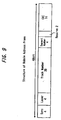
- As described above, the fine clock marks are formed at the same interval on the wobbling address frame .
- FIG. 8 shows a state of the fine clock mark. In each wobbling address frame, 48-bit data is recorded. One bit is, as shown in FIG. 8, expressed by seven waves (carriers) among signals having a predetermined frequency. In one frame, 360 waves exist.
- Assuming that the
optical disk 1 is rotated 1939 times per minute, the frequency of the carrier is 93.1 KHz. - As shown in FIG. 8, in the wobbling address frame shown in FIG. 9, one bit is allocated for each four bits of address information for the fine clock mark. That is, the fine clock mark is superimposed on one bit of four bits which constitute one cycle.
- First one bit in the unit composed of four bits is a bit including the fine clock mark. The residual three bits are bits which do not include the fine clock mark. An enlarged shape of the bit including the fine clock mark is shown in a lower portion of FIG. 8. As shown in the figure, a waveform serving as a fine clock mark FCK is included at the central position of the data bit length.
- The shape of meandering of the
groove 2 on thedisk 1 is formed such that the wobble amplitude WW of the portion corresponding to the fine clock mark FCK is instantaneously enlarged to, for example, about 30 nm. - In one frame, 12 fine clock marks are recorded at intervals of three bits. Therefore, 96 (= 12 × 8) fine clock marks are recorded in one rotation (one track).
- The fine clock mark (a PLL clock which is generated from the fine clock mark in the recording/reproducing apparatus) can be made to be information indicating the circumferential position more precisely than the segment number.
- The frequency of the carrier of each of 48-bit data is a value corresponding to each data. Each data of, for example, the track number or the like, is bi-phase-modulated, and then frequency-modulated. The pre-groove is wobbled with the wave, the frequency of which has been modulated.
- The physical format of the disk according to this embodiment is set as described above. The reason why the foregoing format is set as described above and an obtainable effect thereby will now be described.
- The reason why the track pitch is 0.8 µm, the linear density is 0.35 µm/bit and the wobble amplitude WW is 12.5 nm will now be described.
- Initially, the values that the wavelength of the laser beam satisfies λ = 650 nm and NA = 0.6 as shown in FIG. 1 are considered. Moreover, an assumption is made that a recording capacity of 3 Gbytes is realized in a disk having a diameter of 120 mm.
- Thus, a calculation is performed so that a fact is found that a track pitch of about 0.8 µm is required to realize 3 Gbyte.
- A preferred linear density is considered when a CLD recording operation is performed in a state in which an assumption is made that the track pitch is 0.8 µm.
- FIG. 10 shows a result of measurement of jitters of reproduced data at various linear densities in a state in which the track pitch is 0.8 µm.
- A solid-line curve shows a result in a case where no crosstalk takes place, while one-dot-claim line curve shows a result in a case where crosstalk takes place. The state in which crosstalk takes place is a state in which data is previously recorded on a track adjacent to a track which must be inspected. Therefore, data reproduced from the track which must be inspected contains a certain amount of crosstalk component. The state in which no crosstalk takes place is a state in which data is not recorded on the track adjacent to the track which must be inspected. Therefore, data reproduced from the track which must be inspected does not contain any crosstalk component.
- As can be understood from the foregoing figure, jitters do not increase/decrease rapidly in a direction toward low densities from a boundary which is about a linear density of 0.35 µm/bit. In a portion in which the linear density exceeds 0.35 µm/bit, jitters tend to rapidly increase. That is, a region of the linear density to about 0.35 µm/bit is a preferred region in view of the jitters. Since the density is as raised as possible, the linear density of 0.35 µm/bit is set in this embodiment.
- Then, an amount of the wobble amplitude is considered in a state in which the track pitch is 0.8 µm and the linear density is 0.35 µm/bit.
- FIG. 11 shows the relationship between the C/N (Carrier/Noise ratio) of the wobble and the amount of the wobble amplitude.
- As can be understood from this figure, the C/N is improved in proportion to the amount of the wobble amplitude. That is, in proportion to the amount of the wobble amplitude, the error rate in decoding the absolute address is improved. In proportion to the amount of the wobble amplitude, the C/N deteriorates. Thus, the address error rate deteriorates.
- If the C/N is made to be 23 dB or lower, the address error is made to be a value more than an allowable value. Therefore, the amount of the wobble amplitude must be 10 nm or larger.
- On the other hand, FIG. 12 shows the relationship between the skew margin of the wobble address and the amount of the wobble amplitude. That is, a limit with which the address can satisfactorily be decoded with respect to a state of inclination of the disk is shown. It is preferable that the skew margin is large.
- As can be understood from this figure the skew margin deteriorates when the amount of the wobble amplitude exceeds 15 nm.
- As a result of the above inspection, a preferred amount of the wobble amplitude is 10 nm to 15 nm. In this embodiment, the wobble amplitude WW is made to be 12.5 nm which is included in the above-mentioned range.
- When the amount of the wobble amplitude is determined as described above, whether or not the track pitch of 0.8 µm is an appropriate value is considered.
- Also in this case, the skew margin is employed as the estimation function of the address error.
- FIG. 13 shows the relationship between the track pitch and the address error. FIG. 13 (a) shows a state in which the track pitch is small, while FIG. 13 (b) shows a state in which the track pitch is large. The axis of ordinate stands for the level (%) of the address error and the axis of abscissa stands for a value (degree) of the radial skew.
- Here, the width corresponding to 10 % of the address error is the skew margin. In the case shown in FIG. 13 (a), for example, the skew margin is about ± 0.9°, in the case shown in FIG. 13 (b), the skew margin is about ± 1.2°.
- As can be understood from the figures, the skew margin deteriorates as to the track pitch is narrower.
- FIG. 14 shows skew margins with respect to various track pitches. As shown in the figure, the skew margin deteriorates when the track pitch is made narrower as compared with a portion in which the track pitch is about 0.80 µm.
- From this, it can be understood that the preferred track pitch is about 0.80 µm.
- Although the range from 0.74 µm to 0.82 µm is a permissible range as the skew margin as shown in FIG. 14, the most preferred value among this range is about 0.80 µm.
- That is, as specifications capable of realizing 3 Gbyte, it can be understood that the specification of this embodiment that the track pitch is 0.8 µm, the linear density is 0.35 µm/bit and the wobble amplitude WW is 12.5 nm is one of optimum specifications.
- Therefore, this embodiment is able to realize a format satisfactory to realize a required recording capacity and obtain reliability in extracting the absolute address from the wobbling groove and performing a data decoding operation and the like.
- The disk according to this embodiment and formatted as described above can satisfactorily be driven by a recording/reproducing apparatus while compatibility with, for example, a DVD-ROM is maintained because the contents of the format is identified in the control data.
- As described above, the track pitch and the linear density are, as physical format information in control data, recorded as information of the recording density at the
byte position 3. - As information of the book type at the
byte position 0, a fact that the disk is a disk having specifications that the track pitch is 0.8 µm, the linear density is 0.35 µm/bit and the wobble amplitude WW is 12.5 nm is caused to be identified. - As a matter of course, the book type may also function as information with which the optical disk can be identified. That is, the optical disk is a disk having a structure that the track on which data will be recorded is previously formed as a phase-change recording region, the track is wobbled with a signal obtained by frequency-modulating the carrier having a predetermined frequency in correspondence with address information and wobbling serving as address information is formed in correspondence with the constant angular velocity.
- Further, at the byte positions 33 to 48, recommended information at the first, second and third linear velocities is recorded. As a result of this, a fact is expressed that the disk according to this embodiment employs a peculiar zoning format to be described later to realize the CLD method set to the linear density of 0.35 µm/bit.
- Also the above-mentioned structure enables the disk to be identified that the disk is formatted by a method according to this embodiment.
- A method of cutting the disk having the above-mentioned physical format will now be described.
- A process for manufacturing a disk comprises a so-called master-disk process (a mastering process) and a disk working process (a replication process) in rough classification. The mastering process is a process for completing a metal master (a stamper) for use in the disk working process. The disk working process is a process for mass-producing optical disks which are replicated products by using the stamper.
- Specifically, the so-called cutting is performed in the mastering process which has the steps of coating photoresist on a polished glass substrate and exposing a formed photosensitive film to a laser beam so that a pit and a groove are formed.
- In this embodiment, the pit cutting is performed in a portion corresponding to the emboss area of the disk and the cutting of wobbling groove is performed in a portion corresponding to the groove area.
- Pit data in the emboss area is prepared in a preparing process called a pre-mastering.
- After cutting has been completed, a predetermined processes including development or the like is performed. Then, information is transferred to the metal surface by, for example, electrocasting, so that a stamper required to manufacture disks by replication is manufactured.
- Then, the stamper is used to transfer the information on a resin substrate by, for example, an injection method or the like, and a reflecting film is formed thereon. Then, a process for working the substrate into a required shape of the disk is performed so that final products are manufactured.
- The cutting apparatus, for example, as shown in FIG. 15, is formed of an
optical unit 70 for irradiating a laser beam on aglass substrate 71 having the photoresist to thereby perform the cutting; a drivingunit 80 for rotating theglass substrate 71; and a signal-processingunit 60 for converting inputted data into recording data and controlling theoptical unit 70 and the drivingunit 80. - The
optical unit 70 incorporates a laser-beam source 72 which is made of, for example, a He-Cd laser; an acoustic-optical modulator 73 (AOM) for modulating (on/off) a laser beam emitted from the laser-beam source 72 in accordance with recording data; an acoustic-optical deflector 74 (AOD) for deflecting the laser beam emitted from the laser-beam source 72 in response to a wobbling signal; aprism 75 for bending the optical axis of the modulated beam transmitted from theoptical deflector 74; and anobjective lens 76 for converging the modulated beam reflected by theprism 75 to irradiate the modulated beam on the photoresist surface of theglass substrate 71. - The driving
unit 80 incorporates amotor 81 for rotating theglass substrate 71; anFG 82 for generating an FG pulse for detecting the rotational speed of themotor 81; aslide motor 83 for sliding theglass substrate 71 in the radial direction of the glass substrate; and aservo controller 84 for controlling the rotational speeds of themotor 81 and theslide motor 83 and the tracking of theobjective lens 76 and so on. - The signal-processing
portion 60 incorporates aformatting circuit 61 for adding, for example, an error correction code or the like to source data supplied from, for example, a computer so as to form input data; alogic calculating circuit 62 for subjecting the data supplied from theformatting circuit 61 to a predetermined calculation so as to form recording data; a wobbling-signal generating circuit 63 for generating a wobble signal for wobbling the groove; a mark-signal generating circuit 64 for generating a signal for forming the fine clock mark; a synthesizingcircuit 65; an drivingcircuit 68 for driving theoptical modulator 73 and theoptical deflector 74 in response to a signal supplied from the synthesizingcircuit 65; aclock generator 66 for supplying a clock to thelogic calculating circuit 62 and so forth; and asystem controller 67 for controlling theservo controller 84 and so forth in response to the supplied clock. - When the cutting process is carried out by the cutting apparatus, the
servo controller 84 causes themotor 81 to rotate theglass substrate 71 at a constant angular velocity, as well as theslide motor 83 to slide theglass substrate 71 in such a manner that a spiral track is formed at a predetermined track pitch while the rotation of theglass substrate 71 is maintained. - Simultaneously, a laser beam emitted from the laser-
beam source 72 is allowed to pass through theoptical modulator 73 and theoptical deflector 74 so as to be formed into a modulated beam in accordance with the recording data, and then irradiated on the photoresist surface of theglass substrate 71 from theobjective lens 76. Thus, the photoresist is exposed to the light in accordance with the data and the groove. - On the other hand, the input data to which the error correction code and so forth are added by the
formatting circuit 61, that is, data such as control data or the like, which is recorded on the emboss area is supplied to thelogic calculating circuit 62 so as to be formed into record data. - At timing at which cutting of the emboss area is performed, the record data is supplied to the driving
circuit 68 through the synthesizingcircuit 65. The drivingcircuit 68 controls theoptical modulator 73 to turn on the same at a bit timing at which a pit must be formed in accordance with the record data. At a bit timing at which no pit is formed, theoptical modulator 73 is controlled so as to be turned off. - At the cutting timing for the groove area, the synthesizing
circuit 65 synthesizes a signal corresponding to the fine clock mark transmitted from the mark-signal generating circuit 64 with a signal transmitted from the wobbling-signal generating circuit 63, that is, a signal obtained by frequency-modulating the absolute address so as to supply the same to the drivingcircuit 68 as a signal for forming the wobbling. The drivingcircuit 68 controls theoptical modulator 73 to continuously be turned on for forming the groove. Moreover, the drivingcircuit 68 operates theoptical deflector 74 in response to the signal supplied for the wobbling. As a result, the laser beam is allowed to meander so that the portions which will be exposed to light as grooves are wobbled. - As a result of the above-mentioned operation, exposed portions corresponding to the grooves/emboss pits are formed on the
glass substrate 41 in accordance with the format. - Then, developing, electrocasting and so on are performed so that a stamper is manufactured. By using the stamper, the foregoing disk is manufactured.
- The wobbling-
signal generating circuit 63 and the mark-signal generating circuit 64 provided for the purpose of forming the wobbling grooves including the absolute addresses will now be described. - FIG. 16 shows an example of the structure of the wobbling-
signal generating circuit 63 for generating the wobbling signal for wobbling the grooves. - A generating
circuit 11 generates a signal having a frequency of 372.4 KHz. - The signal generated by the generating
circuit 11 is supplied to a dividingcircuit 12 so as to be divided with a value "15". Then, the result of the division is, as a bi-phase clock signal having a frequency of 24.8 KHz, supplied to a bi-clock signal having a frequency of 24.8 KHz, supplied to abi-phase modulating circuit 13. Moreover, thebi-phase modulating circuit 13 is supplied with ADIP (ADdress In Pre-groove) data as address data. - The
bi-phase modulating circuit 13 bi-phase-modulates the bi-phase clock supplied from thedivider 12 with the ADIP data supplied from a circuit (not shown) so as to transmit a bi-phase signal to anFM modulating circuit 15. - Moreover, the
FM modulating circuit 15 is supplied with a carrier obtained by dividing the signal generated by the generatingcircuit 11 and having the frequency of 372.4 KHz with a value "4" by adivider 14, the carrier having a frequency of 93.1 KHz. - The
FM modulating circuit 15 frequency-modulates the carrier supplied from thedivider 14 with the bi-phase signal supplied from thebi-phase modulating circuit 13. Then, the FM modulating circuit outputs an obtained FM signal, that is, as a wobble signal containing the absolute address to the synthesizingcircuit 65. - As a result of the above-mentioned cutting apparatus, the right and left side walls of the
groove 2 of thedisk 1 are formed (wobbled) in correspondence with the wobble signal formed by the frequency modulation. - FIGS. 17 and 18 show an example of the bi-phase signal outputted from the
bi-phase modulating circuit 13. - In this example, when the preceding bit is 0, "11101000" is employed as the synchronizing pattern (SYNC) as shown in FIG. 17, while when the preceding bit is 1, "00010111" having an opposite phase to that shown in FIG. 17 is employed as the synchronizing pattern. The synchronizing pattern (SYNC) is a unique pattern which does not appear by the modulation and which does not abide by the rule.
- As shown in the figures, "0" of the data bits of the absolute address data (ADIP data) is bi-phase-modulated so as to be converted into channel bit "11" (when the previous channel bit is 0) or "00" (when the previous channel bit is 1).
- "1" in the data bit is converted into channel bit "10" (when the previous channel bit is 0) or "01" (when the previous channel bit is 1).
- Whether conversion to either of the two patterns depends on the previous code. That is, "Wave Form" shown in FIGS. 17 and 18 shows the patterns of the
channel bits - As shown in FIG. 19, the
FM modulating circuit 15 frequency-modulates the carrier supplied from thedivider 14 in correspondence with the bi-phase signal as shown in FIG. 17 or FIG. 18. - That is, when the channel bit data (the bi-phase signal) is "0", the
FM modulating circuit 15 outputs 3.5 waves of the carrier in a period corresponding to the half length of the one data bit. The 3.5 waves of carrier start at a half positive wave or a half negative wave. - When the channel bit data (the bi-phase signal) is "1", on the contrary four waves of carrier are outputted in a period corresponding to the half length of one data bit. Also the four waves of the carrier start at half positive wave or half negative wave.
- Accordingly, when the channel data bit "00" is supplied to the
FM modulating circuit 15 in correspondence with data bit "0", theFM modulating circuit 15 outputs seven waves (= 3.5 + 3.5) of frequency modulation wave in a period corresponding to the length of the data bit. When channel data bit "11" is supplied, the circuit outputs eight waves (= 4 + 4) of frequency modulation wave. - When the channel data bit "10" or "01" is supplied in correspondence to the data bit "1", 7.5 waves (= 4 + 3.5 = 3.5 + 4) of frequency modulation wave are outputted.
- The carrier having the frequency of 93.1 KHz which is supplied to the
FM modulating circuit 15 corresponds to 7.5 waves. TheFM modulating circuit 15 corresponds to data so as to generate 7.5 waves of carrier or seven or eight frequency modulation waves obtained by shifting the same waves by ± 6.20 %. - As described above, either of the carriers corresponding to the
channel data 0 and thechannel data 1, starting at half positive wave and half negative wave respectively and continued from the previous signal, is selected. - FIG. 20 shows an example of frequency modulation wave thus outputted from the
FM modulating circuit 15. In this example, the first data bit is made "0" and its channel data bit is made "00". with respect to the first channel data bit "0", 3.5 waves of carrier starting at the beginning point with the half positive wave have been selected. - As a result, the carrier is ended at the half positive wave. Then, 3.5 waves starting with the half negative wave are selected with respect to the next channel data bit "0". Thus, seven frequency modulation waves with respect to data bit "0" are selected.
- Data bit "1" (channel bit "10") follows the data bit "0". Since 3.5 waves of channel data bit "0" corresponding to the previous data bit "0" are ended with the half negative wave, a carrier starting with the half positive wave is selected as four carrier waves of the carrier of the first channel data bit "1" corresponding to data bit "1". Since the four waves of channel data bit "1" are ended with the negative half wave, a wave starting with the half positive wave is selected as the following four waves of channel data bit "0".
- Then, a similar process is performed so that 7.5 waves, 8 waves and 7 waves of carriers corresponding to data bit "1" (channel data bit "10"), data bit "0" (channel data bit "11") and data bit "0" (channel data bit "00") are formed and outputted in such a manner that the carriers are continued at the boundary (at start and end points).
- As shown in FIG. 20, this embodiment has a structure that the length of the channel bit is an integral multiple of 1/2 of the wavelength of the carrier in any of 7 waves, 7.5 waves and 8 waves of carriers. That is, the length of the channel bit is seven
times 1/2 of the wavelength of the seven waves of carriers (frequency modulation waves) and eighttimes 1/2 of the wavelength of the eight waves of carriers (frequency modulation waves). The length of the channel bit is seven times (when the channel bit is "0") or eight times (when the channel bit is "1") 1/2 of the wavelength of the 7.5 waves of carriers. - In this embodiment, the boundary portion (start or end point) of the bi-phase-modulated channel bit is made to be a zero-cross point of the frequency modulation wave. As a result, the phase of address data (channel bit data) and that of the FM wave are made coincide with each other. Thus, the boundary portion of the bits can easily be distinguished. Therefore, erroneous detection of the address data bit can be prevented. As a result, the address information can easily accurately be reproduced.
- In this embodiment, the boundary portion (start and end points) of data bits and the edge (the zero-cross point) of the frequency modulation wave correspond to each other. As a result, a clock can be generated in such a manner that the edge of the frequency modulation wave is used as a reference.
- In this embodiment, by the way; as shown in FIGS. 21 (a) to 18 (d), when the channel bit data is "00" (data "0"), "11" (data "0"), "10" (data "1") or "01" (data "1"), a fine clock mark having a frequency higher than the frequency modulation frequency (93.1 KHz) of address information is synthesized at the zero-cross point of the carrier at the center (switch point of the channel bit) of respective data.
- FIG. 21 shows a wobble signal having fine clock marks added at every four data bits. The synthesizing
circuit 65 synthesizes a signal supplied from the mark-signal generating circuit 64 to the wobble signal (the frequency modulation wave) supplied from the wobbling-signal generating circuit 63 so as to generate a signal as shown in FIG. 21 at a rate of one time per four bits. - At this time, the fine clock mark is inserted into the zero-cross point of the wobbling frequency modulation wave corresponding to the center (the switching point of the channel data bit) of the address data bit. Thus, fluctuation in the amplitude of the fine clock mark can be reduced and thus the fine clock mark can easily be detected.
- If frequency modulation is performed by the above-mentioned
FM modulating circuit 15 such that the frequency is shifted from the central frequency by - 5 % when the channel data bit is zero and when the frequency is shifted from the central frequency by + 5 % when the channel data bit is 1, the boundary portion of the data bit or the channel data bit and the zero-cross point of the frequency modulation wave do not coincide with each other. Therefore, the channel data bit (or the data bit) can easily be detected erroneously. The insertion point of the fine clock mark is not always the zero-cross point. The fine clock mark is superimposed on a point of the frequency modulation wave having a predetermined amplitude value. As a result, the level of the fine clock mark is raised or lowered by a quantity corresponding to the amplitude value. Thus, a phenomenon is realized in that the detection thereof become difficult. - However, this embodiment with which the fine clock mark is disposed at the position of the zero-cross point of the frequency modulation wave realizes an advantage that its detection or identification from the frequency modulation wave can easily be performed.
- The logical format of data to be recorded will now be described.
- In this embodiment, one cluster is constituted by 32 Kbytes. The cluster is used as a unit when data is recorded. The 32 Kbytes correspond to the above-mentioned ECC block.
- One cluster is constituted by 16 sectors.
- As shown in FIG. 22, data of 2 Kbyte (2048 bytes) is extracted as data for one sector, and then a 16-byte overhead is added to data for one sector. The overhead includes a sector address (an address generated or read by an address
generation reading circuit 35 to be described later with reference to FIG. 37), an error detection code for detecting an error and so on. - Data of 2064 (= 2048 + 16) bytes in total is data (one sector) in 12 × 172 (= 2064) bytes formed into one line shown in FIG. 23.
- Sixteen data for one sector are collected so that data in a quantity of 192 (= 12 × 16) × 172 bytes shown in the figure is constituted.
- A 10-byte internal code (PI) and a 16-byte external code (PO) are added to the data in the quantity of 192 × 172 bytes such that the codes are added to each of bytes in the horizontal and vertical directions as parities.
- Among thus-formed data blocked into 208 × 182 bytes (= (192 + 16) × (172 + 10)) in total, the external code (PO) in a quantity of 16 × 182 bytes is sectioned into sixteen data in a quantity of 1 × 182 bytes. As shown in FIG. 24, each data is added to a portion below 12 × 182 byte sixteen sector data having No. 0 to No. 15 so as to be interleaved.
- Then, data in a quantity of 13 (= 12 + 1) × 182 bytes is made to be data for one sector.
- Data shown in FIG. 26 and having a quantity of 208 × 182 bytes is, as shown in FIG. 25, sectioned into two sections in the vertical direction so that one frame is constituted by 91 byte data so that 208 (row) × 2 (frame) data is formed.
- A 13 (row) × 2 (frame) linking section (data of link area) is added to the leading end of each data in a quantity of 208 × 2 frames.
- More accurately, a portion of the linking section data for 26 frames is recorded at the last of the previous cluster as described later with reference to FIG. 31. The other portion is recorded at the head of the present cluster.
- Moreover, a 2-byte frame synchronizing signal (FS) is further added to the head of the 91-byte frame data. As a result, data for one frame is made to be 93-byte data as shown in FIG. 25. Thus, 221 (row) × 93 × 2 bytes in total, that is, data for a block for 442 frames is formed.
- The foregoing data is made to be data for one cluster (the block which is a unit for recording). The size of actual data portion except for the overhead portion is 32 Kbytes (= 2048 × 16/1024 Kbytes).
- As described above, one cluster is constituted by 16 sectors and one sector is constituted by 26 frames.
- The foregoing data is recorded on the
disk 1 at the cluster unit. The linking section shown in FIG. 26 is disposed between the cluster and the cluster. - The linking section is constituted by 26 frames, that is, the size of the linking section is the same as that of the above-mentioned one sector.
- The linking section is inserted into the portion between the 32 Kbyte clusters (the blocks).
- In actual, division at a linking point is performed at the end of recording operation of the cluster which is block (N) and the recording start point of block (N + 1).
- FIG. 27 shows the types (SY0 to SY7) of the synchronizing signal for each frame of the linking section and the contents of data.
- As shown in the figure, AUX data is sometimes recorded in a predetermined frame as well as all zero data. The portion is sometimes used for controlling the laser power. The types of the frame synchronizing signal will be described later.
- FIG..28 shows a state of the linking section which is formed between the clusters.
- Data such as Slice/PLL data and data such as frame synchronizing signals SY1 to SY7 and the like are, as the linking section (the portion following the linking point) which is formed at the head portion of the 32 Kbyte data block, recorded on each cluster. Postamble PA and postguard regions are formed next to the 32 Kbyte data block which is the main body of the cluster as the linking section (the portion more before the linking point) at the rear end side of the cluster.
- Slice data is data for use to set a time constant for binary-coding reproduced data, while PLL data is data for reproducing the clock.
- As for the frame synchronizing signals (frame sync) SY1 to SY7, any one of
states 1 to 4 is selected and added as described later with reference to FIG. 31. - Data for adjusting the length of the mark for final data and returning the polarity of the signal is recorded in the postamble PA.
- The postguard is an area for absorbing recording jitters which are generated because of eccentricity of the disk, the recording sensitivity of the disk and so on. The postguard has a function for preventing interference of data with a link area on which data will be recorded next even if the data recording start position is changed as described later. The postguard is recorded such that only eight bytes overlap next data when no jitter takes place and DPS (Data Position Shift) to be described later is 0 byte.
- The synchronizing signal (sync) is 4 byte data and a signal for establishing the synchronization. Final four bytes of the linking section are maintained (reserved) for future use.
- Recording of information on each cluster is started at the linking point. When the recording exceeds (overlaps) the linking point by eight bytes, the recording is completed. When recording is performed, the recording/reproducing
circuit 33 of a recording/reproducing apparatus to be described later randomly selects any one ofvalues 0 byte to 64 bytes as DPS. In accordance with the value of the selected DPS, the recording positions for data in the link area and 32 Kbyte block data are changed. - If 0 byte is selected as the DPS as shown in FIG. 28 which is an enlarged view, 14-byte link data is added to a position in front of the first frame synchronizing signal SY1 of the forward linking section. Moreover, 85-byte link data is added to a position in the rear of the final frame synchronizing signal SY5 of the rearward linking section.
- If 32 bytes are selected as the DPS, 46-byte link data is added to the position in front of the first frame synchronizing signal SY1 of the forward linking section. Moreover, 53-byte link data is added to the position in the rear of the final frame synchronizing signal SY5 of the rearward linking section.
- Further, when 64 bytes are selected as the DPS, 78-byte link data is added to the position in front of the first frame synchronizing signal SY1 of the forward linking section. Moreover, 21-byte link data is added to the position in the rear of the final frame synchronizing signal SY5 of the rearward linking section.
- As described above, in accordance with the value of the DPS which is selected by the recording/reproducing
circuit 33, the positions at which link data and 32 Kbyte data block are recorded are changed. - Thus, when information is recorded on a phase-change disk, repeated recording of the same data (for example, the frame synchronizing signal and so on) on the same portion of the disk can be prevented. As a result, the lifetime of the disk, which is evaluated by the number of repeated recording number of times, can be elongated.
- Since the linking point is fixed at that time, generation of the recording timing can be performed similarly to the conventional structure.
- Each frame constituting the cluster/sector is added with the frame synchronizing signal at the head position thereof including the frame of the above-mentioned linking section. The types of the frame synchronizing signals are SY0 to SY7.
- FIG. 29 shows the structure of a frame synchronizing signal for a ROM disk (for example, a DVD-ROM) which can compatibly be used with the disk according to this embodiment in the recording / reproducing apparatus of the present embodiment described later. Also the ROM disk has the structure that one sector is composed of data in 13 rows (lines), that is, 26 frames. Moreover, the frame synchronizing signals (SY0 to SY7) are added to the head of each frame. Note that the ROM disk has no linking section.
- Frame synchronizing signals are set in each of 26 frames starting from the leading frame as SY0, SY5, SY1, SY5, SY2, SY5,..., SY3, SY7, SY4 and SY7 as shown in the figure.
- On the other hand, the structure of the frame synchronizing signal of the disk according to this embodiment is shown in FIG. 30. One sector is composed of 13 rows (lines), that is, 26 frames. The frame synchronizing signals (SY0 to SY7) are added to the head of each frame. Also the linking section has a size corresponding to one sector.
- In each sector and the linking section, frame synchronizing signals are set in each of 26 frames starting from the leading frame as SY0, SY5, SY1, SY5, SY2, SY5,..., SY3, SY7, SY4 and SY7 as shown in the figure.
- From a viewpoint of the sector unit, in the ROM disk and the disk according to this embodiment, the types of the frame sync are the same pattern (arrangement) including the linking section.
- As a result of the above-mentioned structure, the RAM disk can be reproduced by a reproducing apparatus adapted to only the ROM disk.
- That is, the reproducing apparatus adapted to only the ROM disk is arranged such that when the eight frame synchronizing signals SY1, SY7, SY2, SY7, SY3, SY7, SY4 and SY7 stored from the tenth row to the thirteenth row of the data block are detected, a fact that next data is the head portion of the data block is arranged to be recognized. Therefore, the eight frame synchronizing signals are stored in the link area so that the head portion of the data area following the link area can be recognized by the reproducing apparatus.
- FIG. 31 shows an example of the frame synchronizing signals SY0 to SY7. Although the frame synchronizing signal is two-byte data, the length of each frame synchronizing signal is 32 bits (4 bytes) because data already converted into channel bit data is shown in this embodiment.
- For example, four types of
states 1 to 4 exist in SY0. Data of a state is selected with which a DSV (Digital Sum Value) is minimized when addition to frame data in a quantity of 91 bytes (see FIG. 25) is performed. Thus, the selected data is added as the frame synchronizing signal. - As described above, the linking section is a region having an area corresponding to one sector. As a result of the above-mentioned format, the following effects can be obtained.
- The linking section has another function serving as an area for establishing synchronization with recording or reproducing clock prior to performing recording or reproducing actual data as the cluster. Therefore, the linking section is required to have a sufficiently large size to generate the clock for use in the recording/reproducing apparatus.
- In general, the PLL circuit for extracting a reproducing clock has a somewhat long time constant in order to prevent disturbance of the clock occurring because of a damage of the surface of the disk and so on. Therefore, the determined size of the linking section corresponding to one sector is a preferred length in view of generating the clock. That is, the foregoing length is a preferred length when the disk according to this embodiment is reproduced by any one of various reproducing apparatuses (for example, the DVD-ROM player) or the like.
- Since the linking section has the size corresponding to the one sector, also the signal processing system in the recording/reproducing apparatus is not required to perform a complicated process.
- That is, the process for reproducing data is performed such that data in one sector unit is performed and error correction is performed in a block as shown in FIG. 25. If the size of the linking section is not one sector, data read from a disk is, in a data unit smaller than one sector, shifted in a quantity corresponding to the linking section. As a result, the circuit structure and the operation become too complicated. This embodiment having the structure that the linking section is considered as data for one sector is able to simplify the process for omitting, for example, data relating to the linking section from data to be read and a process for generating the linking section data when the recording operation is performed.
- The disk according to this embodiment realizes the CLD method by zone CLD in which zone division into a multiplicity of sections is performed.
- The zoning format will now be described.
- As shown in FIG. 32, the disk according to this embodiment is sectionedinto a plurality of zones (in this case, m + 2 zones from the 0 the zone to the m + 1 the zone) to record or reproduce data.
- Assuming that the number of data frames (the data frames are different from the address frames described with reference to FIG. 9 and are units of blocks of data described with reference to FIG. 25) per track in the 0 the zone is n, the number of data frames per tack is (n + 1) in a next first zone.
- Then, similarly in a zone on more outer peripheral side, the number of data frames increases by one as compared with the adjacent inner peripheral side zone. In the m the zone, the number of data frames is (n + m) and that in the outermost peripheral zone, that is, the (m + 1) the zone, the number of data frames is n + (m + 1).
- The zone is branched at the radial position at which a capacity of (n + 1) frames can be obtained at the innermost peripheral linear density which is the same as that of the previous zone. That is, the radial position at which the capacity of (n + 1) frames can be obtained at the same linear density which is the same as the innermost peripheral linear density in the 0 the zone is the start point for the first zone.
- Similarly, the start position of the m the zone is the radial position at which the capacity of (n + m) frames can be obtained at the same linear density as the innermost peripheral linear density of the 0 the zone.
- When the
disk 1 according to this embodiment has the diameter of 120 mm, the recordable area formed from the radial position of 24 mm to 58 mm, the track pitch of 0.80 µm and the linear density of 0.351 µm/bit, the recordable area is zoned into 815 zones from the 0 the zone to the 814 the zone, as shown in FIG. 33. - In the 0 the zone which starts at the radial position of 24 mm, one track (one rotation) has 578 frames. One frame per track is each increased when the zone is incremented by one each.
- As described above, this embodiment has the structure that one sector is composed of 26 frames (data frames). Therefore, the number (= 1) of frames which is incremented in each zone is made to be a value smaller than the number (= 26) of the frames constituting one sector. As a result, larger number of zones can be formed with a finer unit. Thus, the capacity of the
disk 1 can be enlarged. The above-mentioned method is called a Zoned CLD (Zoned Constant Linear Density). - When the CLD method is employed, the frequency of the clock must linearly be changed in correspondence with the radial position of the disk as indicated with a solid line shown in FIG. 34. However, the foregoing control cannot easily be performed (which is not impossible) and the same is not required in actual. Therefore, this embodiment has a structure that the frequency of the clock is changed in a stepped manner as schematically indicated with a dashed line. Thus, a method basically similar to the Zoned CAV is employed. However, the zone is sectioned into a multiplicity of, for example, 815 zones so that the amount of change in the linear density within the zone is reduced. Thus, as the Zoned CLD method, the linear density is made to be a substantially constant value of about 0.35 µm/bit as a center.
- Detailed parameters for each zone are shown in FIGS. 35 and 36. All of the parameters for all of 815 zones are omitted from description. Then, as to the 0 th zone to
th 23 th zone and as to the 796 th zone to the 814 th zone are shown as examples. - Referring to FIGS. 35 and 36, data on each of the rows indicates each of the zone number, the radial position which is the zone start position, the number of frames per track, the number of tracks per zone, the number of recording/reproducing unit (block) number (the number of clusters) per zone, the linear density within the zone, the capacity of the zone, the rotational speed in the zone, the minimum linear velocity of the zone and the maximum linear velocity of the zone.
- As described above, the zoning like the CLV is performed so that change in the frequency of the clock between a zone and the next zone can be made small. Even if the disk according to this embodiment is reproduced by a reproducing apparatus adapted to only the CLV, a clock can be extracted between zones in which the frequency of the clock is changed. Therefore, the portion between zones can continuously be reproduced.
- FIG. 37 shows an example of the structure of an apparatus for recording/reproducing an optical disk for recording/reproducing data to and from the above-mentioned
disk 1. - A
spindle motor 31 rotates thedisk 1 at a predetermined speed, that is, performs the CAV rotation. - An
optical head 32 irradiates thedisk 1 with a laser beam so that data is recorded on thedisk 1 and reproduces data in accordance with the light reflected from the disk. - A recording/reproducing
circuit 33 causes recording data supplied from an apparatus (for example, a host computer) not shown to temporarily be stored in amemory 34. When data for one cluster, which is a recording unit, has been stored in thememory 34, the recording/reproducing circuit reads data for one cluster therefrom so as to subject read data to encoding, such as interleaving, addition of an error correction code, 8-16 modulation and so on, so as to generate data to be recorded. Then, the recording/reproducing circuit transmits data to be recorded to the optical head so as to cause theoptical head 32 to perform an operation for recording data on thedisk 1. - When a reproducing operation is performed, the recording/reproducing
circuit 33 subjects data obtained from theoptical head 32 to decoding, such as 8-16 demodulation, an error correction process, deinterleaving and so on, so as to output decoded data to the apparatus (not shown). - When a recording operation is performed, an address generating/
reading circuit 35 responds to a control from acontrol circuit 38 comprising, for example, a microcomputer to generate an address (which is not the address to be recorded as wobbling information) which is to be recorded in the track (a pre-groove 2) so as to output the address to the recording/reproducingcircuit 33. - The recording/reproducing
circuit 33 adds the address to data to be recorded so as to output the same to theoptical head 32 to be recorded as the address data. - When address data is included in data reproduced from the track of the
disk 1, the recording/reproducingcircuit 33 separates the address data from reproduced data so as to output the address data to the address generating/reading circuit 35. The address generating/reading circuit 35 outputs the read address to thecontrol circuit 38. - Moreover, the address generating/
reading circuit 35 detects the frame synchronizing signal FS (frame sync) in data so as to output a result of the detection to a frame sync (FS)counter 49. The FS counter 49 counts the number of the FS detection pulses outputted from the address generating/reading circuit 35 and outputs its count value to thecontrol circuit 38. - A
mark detection circuit 36 detects a component corresponding to the fine clock mark from an RF signal (the wobbling signal) reproduced by and outputted from theoptical head 32. A detection signal transmitted from themark detection circuit 36 is supplied to thecontrol circuit 38 and a mark-period detection circuit 40. - A segment-
address detection circuit 37 and a track-address detection circuit 48 detect the segment number and the track number from the wobbling signal outputted from theoptical head 32, respectively. As described above with reference to FIG. 9, the 48-bit wobbling address frame has the track number (the track address) and the segment number (information about the circumferential position). The foregoing numbers are detected by the track-address detection circuit 48 and the segment-address detection circuit 37 and then supplied to thecontrol circuit 38. - The detected track address is also supplied to a
cluster counter 46. - The mark-
period detection circuit 40 determines the periodicity of the detection pulses which are outputted when themark detection circuit 36 has detected the fine clock mark. That is, the fine clock mark is generated at a predetermined cycle (every four bits). Therefore, the mark-period detection circuit determines whether or not the detection pulse supplied from themark detection circuit 36 is a detection pulse generated at the predetermined cycle. If the detection pulse is the detection pulse generated at the predetermined cycle, the mark-period detection circuit generates a pulse synchronized with the detection pulse and outputs the pulse to aphase comparator 42 of aPLL circuit 41 at the rear stage. - If the detection pulse is not supplied at the predetermined cycle, the mark-period detection circuit generates a pseudo pulse at a predetermined timing so as to prevent locking of the following
PLL circuit 41 to an incorrect phase. - The
PLL circuit 41 incorporates, in addition to thephase comparator 42, a low-pass filter 43, a voltage-controlled oscillator (VCO) 44 and adivider 45. - The
phase comparator 42 subjects the phase of an input from the mark-period detection circuit 40 and that of an input from thedivider 45 to a comparison so as to output a phase error therebetween. The low-pass filter 43 compensates for the phase of the phase error signal outputted from thephase comparator 42 so as to output a result of the compensation to theVCO 44. TheVCO 44 generates a clock in the phase corresponding to the output of the low-pass filter 43 so as to outputs the clock to thedivider 45. Thedivider 45 divides the clock supplied from theVCO 44 with a predetermined value and outputs a result of the frequency division to thephase comparator 42. - The clock outputted from the
VCO 44 is, as a recording clock, supplied to a required circuit and also supplied to thecluster counter 46. The cluster counter 46 counts the number of clocks outputtted from theVCO 44 such that the track address in the wobbling signal supplied from the track-address detection circuit 48 is used as a reference. If the counted value thereof reaches a predetermined value (a value corresponding to the length of one cluster), the cluster counter generates a cluster start pulse and outputs the same to thecontrol circuit 38. - A
thread motor 39 is controlled by thecontrol circuit 38 so as to move theoptical head 32 to a predetermined track position on thedisk 1. Thecontrol circuit 38 controls thespindle motor 31 so as to rotate thedisk 1 at a predetermined speed. - A
ROM 47 includes the track number in the address frame, a table for determining the relationship with the zone formed by zoning the data recording region in thedisk 1 and, if necessary, a table for determining the relationship with the zone and the band to which the zone corresponds. - The
control circuit 38 controls the respective units of the apparatus to cause the recording/reproducing operation corresponding to the zoning format to be performed. - When the
control circuit 38 acquires the sector number indicating a point to which an access is made, the control circuit performs a process for replacing the sector number for track number and the data frame number of the track. - That is, in the
ROM 47, a table is stored which shows the sector number, the zone number, as shown in FIG. 39, the ECC block number, the number of frames per zone, the track number, the number of the frames per track and so on. Thecontrol circuit 38 makes a reference to the table to read the track number corresponding to the instructed sector number and the number of data frames in the track. - On the other hand, the
control circuit 38 detects the track number from the output of the track-address detection circuit 48, that is, the present track address which can be detected from the wobbling signal. - When a required (to which an access is made) track number is detected by the track-
address detection circuit 48, thecontrol circuit 38 detects the reference position for the track. - As shown in FIG. 40, the track number serving as the wobbling information is recorded on the
disk 1. Moreover, a clock synchronization mark is recorded in the address frame of each track at a period of four bits. Thecontrol circuit 38 detects the fine clock mark inserted into the first bit of the 48 bits of the first address frame (the address frame having the segment number 0) of a predetermined tack, the fine clock mark being detected as a reference fine clock mark. - When one fine clock mark serving as the reference is detected per round of the track, the
control circuit 38 resets the count of theFS counter 49. Then, the FS counter 49 counts the frame synchronizing signal when it is detected. - If the counted value of the
FS counter 49 becomes to the value corresponding to the sector number which must be retrieved, a determination is made that the sector is the sector which must be retrieved. - When recording in a predetermined sector is performed, the
control circuit 38 controls the recording start position of the recording in the sector to be in a range of (0 to 2) ± 4 bytes from the timing of the zero-cross of the fine clock mark serving as the reference. - As described above, the
control circuit 38 is able to perform control such that an access is made to an arbitrary position (at an arbitrary position in one rotation) on the track from the count value of the recording clock in such a way as to use the clock synchronizing mark which is detected first in the frame (the address frame) having, for example, theframe number 0 as a reference. - That is, the access is permitted in accordance with the track and the data frame unit.
- When an access to an arbitrary position on the track is made as described above, the zone to which the access point belongs must be determined. Moreover, the clock having the frequency corresponding to the zone must be generated by the
VCO 44. Thecontrol circuit 38 performs a clock switching process arranged as shown in a flow chart shown in FIG. 38. - That is, initially, in step F101 the
control circuit 38 reads the track number from the address of the access point outputted from the track-address detection circuit 48. In step F102 the control circuit reads, from the table stored in theROM 47, the zone corresponding to the track number read in step F101. - As described above, the table stored in the
ROM 47 has information about the zone among the 0 the to the 814 the zones to which the tracks having the numbers belong. - In step F103 whether or not the read track number indicates a new zone which is different from the zone to which an access has been made up to now. If a determination is made that the zone is a new zone, the operation proceeds to step F104 so that the
control circuit 38 controls thedivider 45 to cause the frequency division ratio corresponding to the new zone to be set. As a result, recording clocks having frequencies different dependent on the respective zones are outputted from theVCO 44. - If a determination is made in step F103 that the present zone is not a new zone, the process in step F104 is skipped. That is, the frequency division ratio of the
divider 45 is not changed so that the present clock frequency is maintained as it is. - In the process shown in FIG. 38, a reference to the table in the
ROM 47 is made in accordance with the address (the track number) so as to determine the zone. Thus, the clock frequency which must be generated is set. A structure may be employed in which data in the table stored in theROM 47 is not used (that is, it is made unnecessary) and the clock frequency which must be generated is determined by performing a predetermined calculation using the track number so as to set a frequency division ratio. - Although the disk, the adaptable cutting apparatus and the recording/reproducing apparatus according to the embodiment have been described, the present invention is not limited to the foregoing example. As a matter of course, the values about the format may be varied.
- As described above, the optical recording medium according to the invention preferably have the structure that an amount of amplitude of wobbling of the tracks is made to be a value satisfying 10 nm to 15 nm and a track pitch of the track is made to be a value satisfying 0.74 µm to 0.82 µm. The above-mentioned values enable a predetermined data recording capacity on the optical recording medium under a condition of a predetermined NA and laser wavelength. Moreover, the relationship between the amount of the amplitude of wobbling and the track pitch is preferably made to be a value with which a satisfactory reproduction error rate of address information and reproduction information can be obtained. That is, an effect can be obtained in that a new optical recording medium is provided with which large capacity recording can be realized without deterioration in the recording/reproducing performance.
- Moreover, the optical recording medium according to the present invention preferably has the structure that wobbling serving as address information is formed on the track serving as a phase-change recording region in correspondence with constant angular velocity. Moreover, the zoning is set in the track in order to record data at a substantially constant linear density. In addition, an area for recording administration information of the optical recording medium is formed at a predetermined position on the optical recording medium. As the administration information, identification information is recorded which indicates at least a fact that the recording medium is a phase-change recording medium and having the addresses expressed by wobbling tracks. Moreover, recommended information for the recording/reproducing operation at the inner peripheral position and the outer peripheral position is recorded. Thus, an effect can be obtained in that an environment for the recording/reproducing drive can be set to a satisfactory state because of the obtained function for expressing the type of the recording medium, the function for guiding the preferred recording/reproducing operation and the function for realizing the CLD method satisfactorily.
- Since the value of the track pitch and the value of the central linear density are recorded as the administration information and information with which the track pitch and the central linear density can be identified is recorded, the function for identifying the type can be enhanced. Moreover, the recording/reproducing operation can satisfactorily be guided.
- The optical recording medium according to the present invention preferably has the structure that the linking section is disposed between the data block serving as a data recording unit with respect to the track and the adjacent data block. Moreover, the size of data in the linking section is made to be the same as that of the minimum data unit (the sector) constituting the data block. Therefore, the process of the linking section (the process which is performed by the recording/reproducing apparatus) required as the rewritable recording medium can be simplified. Since the foregoing size is sufficiently large to establish the synchronization of the PLL, an effect can be obtained in that the function as the linking section can be enhanced.
- Having described preferred embodiments of the present invention with reference to the accompanying drawings, it is to be understood that the present invention is not limited to the above-mentioned embodiments and that various changes and modifications can be effected therein by one skilled in the art without departing from the scope of the present invention as defined in the appended claims.
Claims (6)
- An optical recording medium (1) in which a track on which data is to be recorded is previously formed and said track is wobbled with a signal obtained from a carrier having a predetermined frequency in correspondence with address information, wherein:said track is formed of a groove (2) having a width larger than that of a land (3) formed adjacent to the groove; andsaid track is a wobbling track having an amplitude amount of more than 10 nm and a track pitch of 0.74 µm to 0.82 µm.
- An optical recording medium as claimed in claim 1, wherein a side wall of said groove (2) is wobbled in accordance with said address information.
- An optical recording medium as claimed in claim 2, wherein said groove (2) has a depth of λ/8 where λ is a wavelength of laser light used to record data on said groove or to reproduce data recorded on said groove.
- An optical recording medium as claimed in claim 2, which has a diameter of about 120mm, a linear density of recorded data of about 0.35 µm/bit, and a recording capacity of at least 3.0 GB.
- An optical recording medium according to any one of the preceding claims, wherein said signal is obtained by frequency-modulating said carrier.
- An optical recording medium according to any one of the preceding claims, wherein said amplitude amount is 10 nm to 15nm.
Priority Applications (1)
| Application Number | Priority Date | Filing Date | Title |
|---|---|---|---|
| EP04078469A EP1538610A3 (en) | 1997-07-24 | 1998-07-22 | Optical recording media and recording thereon |
Applications Claiming Priority (6)
| Application Number | Priority Date | Filing Date | Title |
|---|---|---|---|
| JP198300/97 | 1997-07-24 | ||
| JP19830097 | 1997-07-24 | ||
| JP19830097 | 1997-07-24 | ||
| JP33848997 | 1997-12-09 | ||
| JP33848997A JP4144054B2 (en) | 1997-07-24 | 1997-12-09 | Optical disc recording method |
| JP338489/97 | 1997-12-09 |
Related Child Applications (1)
| Application Number | Title | Priority Date | Filing Date |
|---|---|---|---|
| EP04078469A Division EP1538610A3 (en) | 1997-07-24 | 1998-07-22 | Optical recording media and recording thereon |
Publications (3)
| Publication Number | Publication Date |
|---|---|
| EP0893794A2 EP0893794A2 (en) | 1999-01-27 |
| EP0893794A3 EP0893794A3 (en) | 2001-05-02 |
| EP0893794B1 true EP0893794B1 (en) | 2005-10-12 |
Family
ID=26510900
Family Applications (2)
| Application Number | Title | Priority Date | Filing Date |
|---|---|---|---|
| EP04078469A Withdrawn EP1538610A3 (en) | 1997-07-24 | 1998-07-22 | Optical recording media and recording thereon |
| EP98305833A Expired - Lifetime EP0893794B1 (en) | 1997-07-24 | 1998-07-22 | Optical recording media and recording thereon |
Family Applications Before (1)
| Application Number | Title | Priority Date | Filing Date |
|---|---|---|---|
| EP04078469A Withdrawn EP1538610A3 (en) | 1997-07-24 | 1998-07-22 | Optical recording media and recording thereon |
Country Status (15)
| Country | Link |
|---|---|
| US (1) | US6256282B1 (en) |
| EP (2) | EP1538610A3 (en) |
| JP (1) | JP4144054B2 (en) |
| KR (1) | KR100572810B1 (en) |
| CN (2) | CN1296912C (en) |
| AT (1) | ATE306708T1 (en) |
| AU (1) | AU749969B2 (en) |
| BR (1) | BR9802559A (en) |
| DE (1) | DE69831837T2 (en) |
| DK (1) | DK0893794T3 (en) |
| ES (1) | ES2246523T3 (en) |
| ID (1) | ID20615A (en) |
| MY (1) | MY120337A (en) |
| SG (2) | SG111079A1 (en) |
| TW (1) | TW417105B (en) |
Families Citing this family (48)
| Publication number | Priority date | Publication date | Assignee | Title |
|---|---|---|---|---|
| JP3845849B2 (en) * | 1996-10-18 | 2006-11-15 | ソニー株式会社 | Recording apparatus, recording method, and recording medium |
| WO2000008636A1 (en) * | 1998-08-04 | 2000-02-17 | Koninklijke Philips Electronics N.V. | Optical disc and apparatus for scanning the optical disc |
| JP4491801B2 (en) * | 1999-01-19 | 2010-06-30 | 日本ビクター株式会社 | Recording medium, recording method, recording apparatus, reproducing method, and reproducing apparatus |
| KR100922707B1 (en) * | 1999-01-25 | 2009-10-22 | 코닌클리케 필립스 일렉트로닉스 엔.브이. | Record carrier and apparatus for scanning the record carrier |
| JP2000348347A (en) * | 1999-03-30 | 2000-12-15 | Ricoh Co Ltd | Optical disk |
| WO2001048753A1 (en) | 1999-12-28 | 2001-07-05 | Mitsubishi Chemical Corporation | Rewritable phase change optical disk partly having rom region and data recording and erasing methods for optical disk |
| KR100544175B1 (en) | 1999-05-08 | 2006-01-23 | 삼성전자주식회사 | Recording medium storing linking type information and method for processing defective area |
| DE60038583T2 (en) | 1999-05-19 | 2009-06-04 | Mitsubishi Kagaku Media Co. Ltd. | Rewritable optical recording medium and method for recording EFM-modulated information on the recording medium |
| KR100611953B1 (en) * | 1999-07-07 | 2006-08-11 | 삼성전자주식회사 | Recording medium storing attribute information for basic unit and method for determining data using the attribute information |
| KR100326338B1 (en) * | 1999-09-18 | 2002-03-08 | 구자홍 | Method for recording the data on a optical disc using optimal power |
| CN100336113C (en) * | 1999-10-20 | 2007-09-05 | 皇家菲利浦电子有限公司 | Record-carrier of a read-only type and read device |
| US6430123B1 (en) * | 1999-11-10 | 2002-08-06 | Maxtor Corporation | Scanning micropatterns on an optical medium |
| TW457478B (en) * | 1999-12-16 | 2001-10-01 | Ind Tech Res Inst | Rewritable DVD discs |
| JP3962522B2 (en) | 2000-02-14 | 2007-08-22 | パイオニア株式会社 | Information recording medium |
| TW544671B (en) | 2000-02-25 | 2003-08-01 | Sony Corp | Recording medium, recording apparatus, and reading apparatus |
| US6498773B1 (en) * | 2000-03-15 | 2002-12-24 | Mitsumi Electric Co., Ltd. | Optical disk drive and write speed control method |
| US6990058B1 (en) * | 2000-04-03 | 2006-01-24 | Dphi Acquisitions, Inc. | Structure and method for storing data on optical disks |
| JP2002032922A (en) | 2000-05-12 | 2002-01-31 | Sony Corp | Optical disk and optical unit |
| JP4523117B2 (en) * | 2000-05-31 | 2010-08-11 | 富士通セミコンダクター株式会社 | DATA RECORDING DEVICE, DATA RECORDING METHOD, AND DISC DEVICE |
| US20080123491A1 (en) * | 2000-09-07 | 2008-05-29 | Samsung Electronics Co., Ltd | Optical recording medium having read-only storage area and writeable storage area and recording/reproducing apparatus and method therefor |
| JP4511787B2 (en) * | 2000-10-03 | 2010-07-28 | パナソニック株式会社 | Multilayer optical disc and method for producing multilayer optical disc |
| US7002895B1 (en) * | 2000-11-18 | 2006-02-21 | Hewlett-Packard Development Company, L.P. | Optical disk having zone constant angular velocity wobble |
| EP1833054A3 (en) | 2000-12-26 | 2012-05-16 | Pioneer Corporation | Information recording/reproducing apparatus, and information recording medium |
| KR100475604B1 (en) | 2001-03-09 | 2005-03-10 | 엘지전자 주식회사 | Read only optical disc, and method for reproducing a data in read only optical disc player |
| SK287715B6 (en) * | 2001-04-24 | 2011-07-06 | Koninkl Philips Electronics Nv | Record carrier and method of its manufacturing, recording and/or playback system, method of recording and playing back information |
| JP2003022580A (en) * | 2001-05-02 | 2003-01-24 | Victor Co Of Japan Ltd | Information recording carrier, method of manufacturing information recording carrier, information recording carrier reproducing device and information recording carrier recording device |
| JP4145024B2 (en) * | 2001-05-17 | 2008-09-03 | 富士通株式会社 | Information reproducing apparatus and information recording medium reproducing system |
| US7107299B2 (en) * | 2001-08-14 | 2006-09-12 | Hewlett-Packard Development Company, L.P. | Method and apparatus for managing large numbers of objects having the same property |
| JP2003168222A (en) | 2001-09-20 | 2003-06-13 | Victor Co Of Japan Ltd | Information recording carrier, and reproducing method and device for the same |
| JP2003173543A (en) * | 2001-09-26 | 2003-06-20 | Victor Co Of Japan Ltd | Information recording carrier, and method and device for reproducing the same |
| KR100716962B1 (en) * | 2001-09-29 | 2007-05-10 | 삼성전자주식회사 | Optical disk |
| CN1331122C (en) * | 2002-05-20 | 2007-08-08 | 三星电子株式会社 | Optical disc and method for recording data on the same |
| KR100881665B1 (en) * | 2002-05-31 | 2009-02-06 | 삼성전자주식회사 | Optical information storage medium having plural information recording layer and method of recording/reproducing in the same |
| CA2458609C (en) * | 2002-06-05 | 2013-07-23 | Lg Electronics Inc. | Structure of a linking area formed on a high-density read-only recording medium and manufacturing/reproducing method and apparatus thereof |
| EP1553566B1 (en) * | 2002-07-01 | 2010-05-19 | Panasonic Corporation | Optical disc, optical disc recording device, optical disc recording method |
| KR100727918B1 (en) * | 2002-08-03 | 2007-06-14 | 삼성전자주식회사 | Information storage medium and recording and/or reproducing method thereof |
| RU2290705C2 (en) | 2002-08-03 | 2006-12-27 | Самсунг Электроникс Ко., Лтд. | Information-carrying medium, recording and playback method |
| JP3889365B2 (en) * | 2002-08-12 | 2007-03-07 | パイオニア株式会社 | OPTICAL RECORDING MEDIUM, RECORDING DEVICE, RECORDING METHOD, AND OPTICAL RECORDING MEDIUM MANUFACTURING METHOD |
| JP2004079078A (en) * | 2002-08-19 | 2004-03-11 | Nec Corp | Optical recording medium and its information recording method, recorder |
| JP4130884B2 (en) * | 2002-09-09 | 2008-08-06 | ソニー株式会社 | Playback device and playback method |
| KR100576160B1 (en) * | 2002-12-11 | 2006-05-03 | 엘지전자 주식회사 | Method and apparatus for discriminating record position of high density optical disc |
| KR100750109B1 (en) * | 2003-02-15 | 2007-08-21 | 삼성전자주식회사 | Information storage medium |
| EP1639581A4 (en) * | 2003-06-30 | 2008-12-10 | Samsung Electronics Co Ltd | Information storage medium and method and apparatus for recording and/or reproducing data |
| US8259557B2 (en) | 2004-04-08 | 2012-09-04 | Mitsubishi Electric Corporation | Recording and reproduction control of optical disc, optical disc driving apparatus, optical disc driving method, data processing apparatus, and optical disc recording/reproducing apparatus using version of specification information included in the optical disc |
| CN101095192B (en) * | 2004-09-14 | 2010-05-26 | Lg电子株式会社 | Method and apparatus of recording and reproducing data on the same |
| CN101950567A (en) * | 2006-06-12 | 2011-01-19 | 松下电器产业株式会社 | Reading device and reading method for an optical data recording medium |
| KR101107371B1 (en) | 2010-11-30 | 2012-01-20 | 에스에이치모바일 (주) | Internal capacitance measurement device and method for condenser microphone |
| JP6202337B2 (en) | 2014-03-31 | 2017-09-27 | 株式会社Gsユアサ | Electric storage element and method for manufacturing the same |
Family Cites Families (31)
| Publication number | Priority date | Publication date | Assignee | Title |
|---|---|---|---|---|
| FR2510981B1 (en) * | 1981-08-04 | 1985-10-18 | Kone Ste Fse Ascenseurs | AUTOMATIC HANDLING AND STORAGE EQUIPMENT |
| NL8800255A (en) | 1988-02-03 | 1989-09-01 | Philips Nv | OPTICAL REGISTRATION CARRIER. |
| US5025435A (en) * | 1988-02-03 | 1991-06-18 | U.S. Philips Corporation | Apparatus for reading or writing contrast enhanced information optical record carrier |
| US5185732A (en) * | 1988-06-20 | 1993-02-09 | Sony Corporation | Recording medium and recording and reproducing apparatus employing the recording medium |
| US5270991A (en) * | 1990-06-29 | 1993-12-14 | North American Philips Corporation | Track format for use with an optical record carrier having a varying track pitch |
| JP2809835B2 (en) * | 1990-07-30 | 1998-10-15 | 松下電器産業株式会社 | Optical disk device and optical disk |
| JP3141241B2 (en) * | 1990-08-24 | 2001-03-05 | ソニー株式会社 | Disk recording device and disk reproducing device |
| JP3158474B2 (en) * | 1991-03-28 | 2001-04-23 | ソニー株式会社 | Recording method, disk recording device and disk reproducing device |
| EP0571221B1 (en) * | 1992-05-22 | 1999-09-01 | Sony Corporation | Disc recording apparatus and disc recording method |
| JP3221100B2 (en) * | 1992-10-30 | 2001-10-22 | ソニー株式会社 | optical disk |
| JPH06187732A (en) * | 1992-12-15 | 1994-07-08 | Sony Corp | Magneto-optical disk device and magneto-optical disk |
| JP3440952B2 (en) * | 1993-02-24 | 2003-08-25 | ソニー株式会社 | Data recording method and data reproducing method |
| JPH06309672A (en) * | 1993-04-26 | 1994-11-04 | Sony Corp | Optical disk recording medium and optical disk device |
| JP2860229B2 (en) * | 1993-06-25 | 1999-02-24 | 株式会社ケンウッド | Optical disk recording and playback device |
| JP3145235B2 (en) * | 1993-09-03 | 2001-03-12 | パイオニア株式会社 | Recordable disc, recording device and recording method thereof |
| JP3051016B2 (en) * | 1994-01-20 | 2000-06-12 | 松下電器産業株式会社 | Optical disk medium and clock generation device therefor |
| JP3150850B2 (en) * | 1994-07-08 | 2001-03-26 | シャープ株式会社 | Manufacturing method of magneto-optical disk master |
| JP3480057B2 (en) * | 1994-09-12 | 2003-12-15 | ソニー株式会社 | Data recording method, data reproducing method and recording medium |
| JPH08147699A (en) * | 1994-11-22 | 1996-06-07 | Sony Corp | Information recorder/reproducer |
| US6487151B1 (en) * | 1994-12-20 | 2002-11-26 | Matsushita Electric Industrial Co. Ltd. | Optical information recording and reproducing system with overwrite capability and recording medium for use therewith |
| US6118752A (en) * | 1995-07-07 | 2000-09-12 | Matsushita Electric Industrial Co., Ltd. | Optical information recording medium offset pre-pit array indicating identification information |
| US5703867A (en) * | 1995-07-21 | 1997-12-30 | Hitachi, Ltd. | Optical recording medium having a dummy area at leading and/or trailing positions of recording area |
| US5835479A (en) * | 1995-10-09 | 1998-11-10 | Matsushita Electric Industrial Co., Ltd. | Optical information recording medium |
| JPH09237421A (en) * | 1996-03-01 | 1997-09-09 | Sony Corp | Recording and reproducing device and method |
| JP3703569B2 (en) * | 1996-04-02 | 2005-10-05 | ソニー株式会社 | Optical recording medium, recording / reproducing method thereof, and recording / reproducing apparatus |
| JP2856390B2 (en) * | 1996-07-26 | 1999-02-10 | 株式会社日立製作所 | Information recording medium and recording / reproducing method using the same |
| US5809006A (en) * | 1996-05-31 | 1998-09-15 | Cagent Technologies, Inc. | Optical disk with copy protection, and apparatus and method for recording and reproducing same |
| JPH1069646A (en) * | 1996-08-29 | 1998-03-10 | Ricoh Co Ltd | Optical disk medium, optical disk device |
| EP0977187B1 (en) * | 1996-10-07 | 2001-03-07 | Matsushita Electric Industrial Co., Ltd. | Optical disc, optical disc device, and method for recording an optical disc |
| JP3845849B2 (en) * | 1996-10-18 | 2006-11-15 | ソニー株式会社 | Recording apparatus, recording method, and recording medium |
| CN1516131A (en) * | 1996-10-22 | 2004-07-28 | ������������ʽ���� | Information recording medium and playback device capable of expressing magnetic track swinging information |
-
1997
- 1997-12-09 JP JP33848997A patent/JP4144054B2/en not_active Expired - Lifetime
-
1998
- 1998-07-14 TW TW087111446A patent/TW417105B/en not_active IP Right Cessation
- 1998-07-21 SG SG200204860A patent/SG111079A1/en unknown
- 1998-07-21 SG SG9802480A patent/SG89261A1/en unknown
- 1998-07-21 US US09/120,416 patent/US6256282B1/en not_active Expired - Lifetime
- 1998-07-22 DE DE69831837T patent/DE69831837T2/en not_active Expired - Lifetime
- 1998-07-22 ES ES98305833T patent/ES2246523T3/en not_active Expired - Lifetime
- 1998-07-22 EP EP04078469A patent/EP1538610A3/en not_active Withdrawn
- 1998-07-22 AT AT98305833T patent/ATE306708T1/en active
- 1998-07-22 EP EP98305833A patent/EP0893794B1/en not_active Expired - Lifetime
- 1998-07-22 DK DK98305833T patent/DK0893794T3/en active
- 1998-07-23 AU AU77476/98A patent/AU749969B2/en not_active Expired
- 1998-07-23 ID IDP981041A patent/ID20615A/en unknown
- 1998-07-24 BR BR9802559-7A patent/BR9802559A/en not_active Application Discontinuation
- 1998-07-24 MY MYPI98003386A patent/MY120337A/en unknown
- 1998-07-24 CN CNB981243444A patent/CN1296912C/en not_active Expired - Lifetime
- 1998-07-24 KR KR1019980031366A patent/KR100572810B1/en not_active IP Right Cessation
- 1998-07-24 CN CNB2004100325781A patent/CN1311452C/en not_active Expired - Lifetime
Also Published As
| Publication number | Publication date |
|---|---|
| CN1311452C (en) | 2007-04-18 |
| ID20615A (en) | 1999-01-28 |
| DE69831837T2 (en) | 2006-07-06 |
| SG111079A1 (en) | 2005-05-30 |
| JPH1196602A (en) | 1999-04-09 |
| EP0893794A3 (en) | 2001-05-02 |
| ES2246523T3 (en) | 2006-02-16 |
| DE69831837D1 (en) | 2006-02-23 |
| CN1296912C (en) | 2007-01-24 |
| AU7747698A (en) | 1999-02-04 |
| KR19990014335A (en) | 1999-02-25 |
| US6256282B1 (en) | 2001-07-03 |
| MY120337A (en) | 2005-10-31 |
| JP4144054B2 (en) | 2008-09-03 |
| EP0893794A2 (en) | 1999-01-27 |
| AU749969B2 (en) | 2002-07-04 |
| CN1213130A (en) | 1999-04-07 |
| KR100572810B1 (en) | 2006-10-31 |
| EP1538610A3 (en) | 2008-10-22 |
| DK0893794T3 (en) | 2005-11-07 |
| CN1542794A (en) | 2004-11-03 |
| TW417105B (en) | 2001-01-01 |
| EP1538610A2 (en) | 2005-06-08 |
| SG89261A1 (en) | 2002-06-18 |
| BR9802559A (en) | 1999-10-13 |
| ATE306708T1 (en) | 2005-10-15 |
Similar Documents
| Publication | Publication Date | Title |
|---|---|---|
| EP0893794B1 (en) | Optical recording media and recording thereon | |
| JP3845849B2 (en) | Recording apparatus, recording method, and recording medium | |
| US5991257A (en) | Disk with zones of tracks segmented into data frames, with tracks closer to the disk edge having more frames, and a data recording/reproducing method and apparatus using such disk | |
| JP4298793B2 (en) | optical disk | |
| US6256276B1 (en) | Disk recording and reproducing apparatus and method for use in a rewritable type disk | |
| TWI273564B (en) | Recording-medium evaluation method, recording/reproduction apparatus and recording medium | |
| KR100533893B1 (en) | Data recording device and method | |
| JP2005063533A (en) | Information recording medium, recording method for information recording medium and information recording and reproducing device | |
| JP4226204B2 (en) | Optical recording medium, manufacturing apparatus and manufacturing method thereof | |
| KR100605412B1 (en) | Optical recording medium, and method of manufacturing optical recording medium | |
| US6898171B1 (en) | Information recording medium with index header | |
| JP4557272B2 (en) | Recording / reproducing apparatus and method | |
| JP3092707B2 (en) | optical disk | |
| JPH09120585A (en) | Information recording medium, recording control information reproducing method and information recording and reproducing device | |
| AU771022B2 (en) | Optical recording medium and recording method thereof | |
| JPH11283280A (en) | Optical disk, device and method for recording and reproducing optical disk, and device for producing master disk of optical disk | |
| JP3092708B2 (en) | optical disk | |
| JPH11134671A (en) | Reproducing device and method thereof | |
| JP2007122870A (en) | Recording apparatus and method | |
| MXPA98005944A (en) | Medium of optimal registration and method of registration of mi | |
| JP2002042348A (en) | Optical disk, optical disk device, and method for recording /reproducing information | |
| JP2002251838A (en) | Disk, recording and reproducing device and method | |
| JP2005018986A (en) | Optical disk, optical disk recording device, and optical disk recording method | |
| JP2002183977A (en) | Optical disk, optical disk recording device, and optical disk reproducing device |
Legal Events
| Date | Code | Title | Description |
|---|---|---|---|
| PUAI | Public reference made under article 153(3) epc to a published international application that has entered the european phase |
Free format text: ORIGINAL CODE: 0009012 |
|
| AK | Designated contracting states |
Kind code of ref document: A2 Designated state(s): AT BE CH DE DK ES FR GB IT LI NL |
|
| AX | Request for extension of the european patent |
Free format text: AL;LT;LV;MK;RO;SI |
|
| PUAL | Search report despatched |
Free format text: ORIGINAL CODE: 0009013 |
|
| RIC1 | Information provided on ipc code assigned before grant |
Free format text: 7G 11B 7/007 A, 7G 11B 20/12 B |
|
| AK | Designated contracting states |
Kind code of ref document: A3 Designated state(s): AT BE CH CY DE DK ES FI FR GB GR IE IT LI LU MC NL PT SE |
|
| AX | Request for extension of the european patent |
Free format text: AL;LT;LV;MK;RO;SI |
|
| 17P | Request for examination filed |
Effective date: 20011015 |
|
| AKX | Designation fees paid |
Free format text: AT BE CH DE DK ES FR LI |
|
| RBV | Designated contracting states (corrected) |
Designated state(s): AT BE CH DE DK ES FR GB IT LI NL |
|
| 17Q | First examination report despatched |
Effective date: 20040816 |
|
| GRAP | Despatch of communication of intention to grant a patent |
Free format text: ORIGINAL CODE: EPIDOSNIGR1 |
|
| GRAS | Grant fee paid |
Free format text: ORIGINAL CODE: EPIDOSNIGR3 |
|
| GRAA | (expected) grant |
Free format text: ORIGINAL CODE: 0009210 |
|
| AK | Designated contracting states |
Kind code of ref document: B1 Designated state(s): AT BE CH DE DK ES FR GB IT LI NL |
|
| REG | Reference to a national code |
Ref country code: GB Ref legal event code: FG4D |
|
| REG | Reference to a national code |
Ref country code: CH Ref legal event code: EP |
|
| REG | Reference to a national code |
Ref country code: CH Ref legal event code: NV Representative=s name: ISLER & PEDRAZZINI AG |
|
| REG | Reference to a national code |
Ref country code: DK Ref legal event code: T3 |
|
| REG | Reference to a national code |
Ref country code: ES Ref legal event code: FG2A Ref document number: 2246523 Country of ref document: ES Kind code of ref document: T3 |
|
| REF | Corresponds to: |
Ref document number: 69831837 Country of ref document: DE Date of ref document: 20060223 Kind code of ref document: P |
|
| ET | Fr: translation filed | ||
| PLBE | No opposition filed within time limit |
Free format text: ORIGINAL CODE: 0009261 |
|
| STAA | Information on the status of an ep patent application or granted ep patent |
Free format text: STATUS: NO OPPOSITION FILED WITHIN TIME LIMIT |
|
| 26N | No opposition filed |
Effective date: 20060713 |
|
| REG | Reference to a national code |
Ref country code: CH Ref legal event code: PCAR Free format text: ISLER & PEDRAZZINI AG;POSTFACH 1772;8027 ZUERICH (CH) |
|
| REG | Reference to a national code |
Ref country code: DE Ref legal event code: R084 Ref document number: 69831837 Country of ref document: DE |
|
| REG | Reference to a national code |
Ref country code: GB Ref legal event code: 746 Effective date: 20150424 |
|
| REG | Reference to a national code |
Ref country code: DE Ref legal event code: R084 Ref document number: 69831837 Country of ref document: DE Effective date: 20150410 |
|
| REG | Reference to a national code |
Ref country code: FR Ref legal event code: PLFP Year of fee payment: 19 |
|
| REG | Reference to a national code |
Ref country code: FR Ref legal event code: PLFP Year of fee payment: 20 |
|
| PGFP | Annual fee paid to national office [announced via postgrant information from national office to epo] |
Ref country code: NL Payment date: 20170719 Year of fee payment: 20 |
|
| PGFP | Annual fee paid to national office [announced via postgrant information from national office to epo] |
Ref country code: ES Payment date: 20170825 Year of fee payment: 20 Ref country code: DE Payment date: 20170724 Year of fee payment: 20 Ref country code: IT Payment date: 20170728 Year of fee payment: 20 Ref country code: FR Payment date: 20170724 Year of fee payment: 20 Ref country code: CH Payment date: 20170719 Year of fee payment: 20 Ref country code: GB Payment date: 20170719 Year of fee payment: 20 |
|
| PGFP | Annual fee paid to national office [announced via postgrant information from national office to epo] |
Ref country code: DK Payment date: 20170719 Year of fee payment: 20 Ref country code: AT Payment date: 20170720 Year of fee payment: 20 Ref country code: BE Payment date: 20170719 Year of fee payment: 20 |
|
| REG | Reference to a national code |
Ref country code: DE Ref legal event code: R071 Ref document number: 69831837 Country of ref document: DE |
|
| REG | Reference to a national code |
Ref country code: NL Ref legal event code: MK Effective date: 20180721 |
|
| REG | Reference to a national code |
Ref country code: DK Ref legal event code: EUP Effective date: 20180722 |
|
| REG | Reference to a national code |
Ref country code: CH Ref legal event code: PL |
|
| REG | Reference to a national code |
Ref country code: GB Ref legal event code: PE20 Expiry date: 20180721 |
|
| REG | Reference to a national code |
Ref country code: AT Ref legal event code: MK07 Ref document number: 306708 Country of ref document: AT Kind code of ref document: T Effective date: 20180722 |
|
| REG | Reference to a national code |
Ref country code: BE Ref legal event code: MK Effective date: 20180722 |
|
| PG25 | Lapsed in a contracting state [announced via postgrant information from national office to epo] |
Ref country code: GB Free format text: LAPSE BECAUSE OF EXPIRATION OF PROTECTION Effective date: 20180721 |
|
| REG | Reference to a national code |
Ref country code: ES Ref legal event code: FD2A Effective date: 20201203 |
|
| PG25 | Lapsed in a contracting state [announced via postgrant information from national office to epo] |
Ref country code: ES Free format text: LAPSE BECAUSE OF EXPIRATION OF PROTECTION Effective date: 20180723 |