EP0892992B1 - Drei-farbensensor mit einer pin- oder nip-schichtenfolge - Google Patents
Drei-farbensensor mit einer pin- oder nip-schichtenfolge Download PDFInfo
- Publication number
- EP0892992B1 EP0892992B1 EP97922827A EP97922827A EP0892992B1 EP 0892992 B1 EP0892992 B1 EP 0892992B1 EP 97922827 A EP97922827 A EP 97922827A EP 97922827 A EP97922827 A EP 97922827A EP 0892992 B1 EP0892992 B1 EP 0892992B1
- Authority
- EP
- European Patent Office
- Prior art keywords
- layer
- layers
- adjacent
- structure according
- band gap
- Prior art date
- Legal status (The legal status is an assumption and is not a legal conclusion. Google has not performed a legal analysis and makes no representation as to the accuracy of the status listed.)
- Expired - Lifetime
Links
Images




Classifications
-
- H—ELECTRICITY
- H10—SEMICONDUCTOR DEVICES; ELECTRIC SOLID-STATE DEVICES NOT OTHERWISE PROVIDED FOR
- H10F—INORGANIC SEMICONDUCTOR DEVICES SENSITIVE TO INFRARED RADIATION, LIGHT, ELECTROMAGNETIC RADIATION OF SHORTER WAVELENGTH OR CORPUSCULAR RADIATION
- H10F30/00—Individual radiation-sensitive semiconductor devices in which radiation controls the flow of current through the devices, e.g. photodetectors
- H10F30/20—Individual radiation-sensitive semiconductor devices in which radiation controls the flow of current through the devices, e.g. photodetectors the devices having potential barriers, e.g. phototransistors
- H10F30/21—Individual radiation-sensitive semiconductor devices in which radiation controls the flow of current through the devices, e.g. photodetectors the devices having potential barriers, e.g. phototransistors the devices being sensitive to infrared, visible or ultraviolet radiation
- H10F30/22—Individual radiation-sensitive semiconductor devices in which radiation controls the flow of current through the devices, e.g. photodetectors the devices having potential barriers, e.g. phototransistors the devices being sensitive to infrared, visible or ultraviolet radiation the devices having only one potential barrier, e.g. photodiodes
- H10F30/223—Individual radiation-sensitive semiconductor devices in which radiation controls the flow of current through the devices, e.g. photodetectors the devices having potential barriers, e.g. phototransistors the devices being sensitive to infrared, visible or ultraviolet radiation the devices having only one potential barrier, e.g. photodiodes the potential barrier being a PIN barrier
- H10F30/2235—Individual radiation-sensitive semiconductor devices in which radiation controls the flow of current through the devices, e.g. photodetectors the devices having potential barriers, e.g. phototransistors the devices being sensitive to infrared, visible or ultraviolet radiation the devices having only one potential barrier, e.g. photodiodes the potential barrier being a PIN barrier the devices comprising Group IV amorphous materials
-
- H—ELECTRICITY
- H10—SEMICONDUCTOR DEVICES; ELECTRIC SOLID-STATE DEVICES NOT OTHERWISE PROVIDED FOR
- H10F—INORGANIC SEMICONDUCTOR DEVICES SENSITIVE TO INFRARED RADIATION, LIGHT, ELECTROMAGNETIC RADIATION OF SHORTER WAVELENGTH OR CORPUSCULAR RADIATION
- H10F19/00—Integrated devices, or assemblies of multiple devices, comprising at least one photovoltaic cell covered by group H10F10/00, e.g. photovoltaic modules
- H10F19/50—Integrated devices comprising at least one photovoltaic cell and other types of semiconductor or solid-state components
Definitions
- the invention relates to a structure with a plurality of i-layers, that on one side from ap layer the other side is bounded by an n-layer, according to the preamble of claim 1. Furthermore relates to the invention includes such a structure Component, in particular a multi-color sensor based on a pin or nip structure, according to the The preamble of claim 10. Furthermore, the Invention a method for producing such Structure according to the preamble of claim 11.
- Components are known as prior art on the Base of amorphous silicon or its alloys, consisting of two antiserially arranged pin or nip diodes to form a pinip or nipin structure.
- the diodes are essentially vertical arranged to the direction of light incidence.
- Such a nipin structure as a photosensitive electronic Component based on amorphous silicon is known for example from US patent 53 11 047.
- the blue / green sensitivity can be between 1.74 eV and 1.9 eV in the upstream in the direction of light incidence nip structure or the red / green separation in the in Improved direction of light downstream pin structure become.
- a structure is known from WO 96/13865 in which improved spectral selectivity is achieved by the product ⁇ in the direction of light incidence upstream sublayer I is higher than that in in Sub-layer II downstream of light incidence.
- a disadvantage of the known components mentioned are only due to the structure of the layer system to three linearly independent, spectral sensitivity curves detected. Hence one is comparative elaborate superposition of these three independent signals required for color image processing. Farther are comparatively complex, antiserial to each other switched structures to implement the Sensor necessary.
- the invention is therefore based on the object To create structure with multiple i-layers at the independent signals are obtained such that a reduced superposition is required down to Avoiding such a superposition.
- the task is solved by a structure according to the Set of features according to claim 1.
- the task is further solved by a component according to the whole of the features of claim 10.
- the task is further solved by a method according to the whole of the features of claim 11. Further appropriate or advantageous embodiments or variants can be found in each of these claims related subclaims.
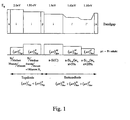
- the respective band gap E g of at least three adjacent i-layers decreases from the direction of incidence of light as a result of a suitable choice of alloys, while the transport properties (which with the aid of the Products ⁇ can be characterized) of the photogenerated charge carriers for a nipin structure in both intrinsic layer systems of the top and bottom diodes in the direction of the p-layer become better (see FIG. 1).
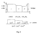
- the band gap of the individual layers is generally reduced by a suitable choice of alloys from the direction of light incidence, while the ⁇ product increases from the n-type layer to both p-type layers.
- the collection of the load carriers can a change in the electrical field (e.g. due to microdoping of the i-layers) to be influenced this way the spatial charge carrier collection continues to vary.
- the structure was not limited to structures of the type nipin or pinip is; rather and also expressly from the invention surprisingly simple structures are also included and components of the structure containing such a structure Type of a simple pin or nip structure. advantageously, With such a structure, only one is sufficient Polarity as opposed to the avoidable for deemed necessary, antiserial switched double diodes of the type of a pinip or nipin structure.
- the structure according to the invention is advantageous in such a way that they detect different light Wavelengths by varying the Structure applied voltage continuously adjustable and thus the required superposition at least diminished.
- FIG. 1 a structure of the nipin type is shown in cross-section with the top and bottom diodes successively formed by the direction of light incidence (from left to right).
- the upper representation shows the course of the band gap E g
- the lower representation shows the course of the transport properties ⁇ as a function of the position coordinate x in the layer sequence.
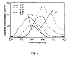
- FIG 2 is an example of a 5-color sensor with a structure according to Figure 1 demonstrates how itself from positive higher voltage (the front diode is the spectral sensitivity of a wavelength of 470 nm (collection of all generated Charge carriers in the front top diode) to 500 nm adjustable for low positive voltages leaves.
- the front diode is the spectral sensitivity of a wavelength of 470 nm (collection of all generated Charge carriers in the front top diode) to 500 nm adjustable for low positive voltages leaves.
- the different ⁇ products are exemplified by the use of materials made with different hydrogen dilution, realized.
- the electrical voltage only increases with higher positive voltages Field above the top diode and the charge carrier pairs can be in the anterior area of intrinsic i-layer of the top diode can be collected.
- the bottom diode is in the reverse direction and the photogenerated charge carriers can be collected in this diode.
- the charge carrier pairs are collected in the range ( ⁇ ) III (maximum of the spectral sensitivity at 550 nm), while in all other ranges (( ⁇ ) IV and ( ⁇ ) V ) they recombine by incorporating material with a shorter lifespan , If you increase the electric field above the intrinsic layer in the bottom diode, you collect the charge carriers in the areas with ( ⁇ ) III and ( ⁇ ) IV , while the photogenerated charge carriers in the area with ( ⁇ ) V continue to recombine (maximum of the spectral sensitivity at 595 nm).
- the manufacturing conditions can affect the transport properties of a-Si: H based alloys in detail have the following influence:
- the optoelectronic Properties by varying the manufacturing conditions influence.
- the material quality by varying the deposition pressure, the temperature, the electrical supplied Performance or by appropriate addition of additional Process gases (e.g. hydrogen, helium, argon, fluorine) be changed during the shift deposition.
- additional Process gases e.g. hydrogen, helium, argon, fluorine
- the transport properties change sometimes very strong, even with the composition of the respective alloy.
- This behavior is based on the example of the silicon germanium alloy shown in Figures 3 to 5.
- the optical bandgap can be continuously adjusted between E G ⁇ 1.8 eV (a-Si: H) and E G ⁇ 1.0 eV (a-Ge: H), as can be seen from the insertion in FIG. 3.
- the defect density determined using the measurement method known as the "Constant Photocurrent Method” increases by two orders of magnitude or more (FIG. 3, large image).
- the photo and dark conductivity (see FIG. 4) and the ambipolar diffusion length (see FIG. 5) change depending on the alloy composition.
- the photoconductivity is proportional to the product of charge carrier life ⁇ and mobility ⁇ and reflects the transport properties of the majority charge carriers (here: electrons).
- the ambipolar diffusion length essentially describes the transport properties of the minority charge carriers (here: holes) for the material here.
- the transport properties of silicon alloys can be influenced by preparative measures (as described above), in particular by adding additional process gases during deposition [Matsuda 1,2].
- hydrogen dilution the influence of hydrogen addition ("hydrogen dilution") to the process gases silane (SiH 4 ) and methane (CH 4 ) is shown in FIG. 6 for the alloy system a-Si 1-x C x : H.
- Material made with strong hydrogen dilution shows a much higher photoconductivity and thus higher values for the ⁇ product than in the cases where deposited material without H 2 addition is used. This effect increases with increasing C (carbon) content in the material.
- the ratio of [H 2 ] to ([SiH 4 ] + [CH 4 ]) can assume values from 10 to 50, for example.
- Figure 7 shows the course of the band gap Eg and Transport properties ⁇ as a function of the coordinate a nip structure according to the invention with three i layers.
- phosphorus Figure 7, curve 1
- Figure 7, curve 2 By incorporating phosphorus (Figure 7, curve 1) positive, fixed charge built into the absorber layer.
- the electric field in the area of p / i transition increases while it is in other part of the Absorber layer (in the area of the i / n transition) reduced becomes.
- the location-dependent collection is carried out supports the location-dependent field course.
- the opposite Influence is observed for the incorporation of boron (Figure 7, curve 2).
- partial doping can also be used individual i-layers of the modified absorber layer (with for example boron, phosphorus, arsenic or Fluorine) the field and thus the wavelength-dependent Collection efficiency can be changed or discontinued.
- the nip according to the invention suitable as a photodiode or pin structure, its spectral sensitivity can be moved by varying the applied voltage enables the formation of a unipolar detector, where only a single polarity of the structure applied voltage is required to the three known (Red, green and blue), other colors or even several to detect these colors.
- a u-nipolar is also realized according to the invention three or more color sensor based a pin or nip structure, especially on the Base of amorphous silicon or its alloys.
- One suitable for the formation of a sensor Structure also has the advantage that when training of a sensor array using such a structure significantly reduced coupling of neighboring pixels occurs, because this structure compared to a nipin or pinip structure no conductive middle layer in Shape of the adjacent on both sides of i-layers has p or n layer.
- this structure compared to a nipin or pinip structure no conductive middle layer in Shape of the adjacent on both sides of i-layers has p or n layer.
- for the created Voltage advantageously only one Polarity needed.
- transient behavior towards a detector on the Base of two antiserial diodes improved because of charging processes of the stored cargo in the top or Bottom diode does not occur, as is the case with pinip or nipin structures observed.
- FIG. 9 shows measurement results for a structure according to FIG. 8, which show the shift in the spectral sensitivity and its split adjustability as a function of the wavelength of the light for increasing negative voltage.
- the band gap is determined by the Direction of light incidence (n-layer) also reduced, while the transport properties in the three different areas from the n-layer to the p-layer getting better.
- the high conductivity of doped n and p layers leads to coupling currents perpendicular to the direction of light incidence in unstructured sensor arrays or sensor rows.
- the area of an active pixel in an unstructured sensor array is defined by its back contact (structured metallization level).
- An occurring coupling current (I q ) is superimposed on the photocurrent and impedes or prevents the evaluation of the signal.
- Coupling processes over the n-layer (last semiconductor layer before the back contact) with a nipin or pin diode (with a pinip detector the p-layer accordingly) can be achieved by technological measures (e.g.
- the coupling via the p-layer in a nipin detector can only be achieved by a complete structuring (removal of the thin-film system between individual pixels) of the array or by the transition to a unipolar one Prevent detector (pin or nip diode) in which the complex i-layer system in the component is not interrupted by a layer with high conductivity. Since the structuring of the complete array is technologically complex and cost-intensive, an unstructured sensor array made of pin or nip diodes, which can separate three or more spectral components of the light, is an advance in terms of reducing the coupling current.
Landscapes
- Light Receiving Elements (AREA)
- Solid State Image Pick-Up Elements (AREA)
- Investigating Or Analysing Biological Materials (AREA)
- Investigating Or Analysing Materials By The Use Of Chemical Reactions (AREA)
- Spectrometry And Color Measurement (AREA)
Description
- Fig. 1:
- örtlicher Verlauf der Bandlücke Eg und des Produkts µτ einer zur Bildung beispielsweise eines Farbsensors geeigneten, erfindungsgemäßen nipin-Struktur;
- Fig. 2:
- spektrale Empfindlichkeit einer nipin-Struktur nach Figur 1;
- Fig. 3:
- Defektdichte ND als Funktion des optischen Bandabstandes für a-Si1-xGex:H, wobei in der Einfügung der optische Bandabstand als Funktion des Germaniumgehaltes im Material dargestellt ist;
- Fig. 4:
- Photo- ((O) bzw. AM 1.5) und Dunkelleitfähigkeit (•) σ als Funktion des optischen Bandabstandes Eg für a-Si1-xGex:H;
- Fig. 5:
- ambipolare Diffusionslänge Lambi als Funktion des optischen Bandabstandes Eg für a-Si1-xGex:H im Vergleich zu aus der Literatur bekannten Werten [3, 4, 5] ;
- Fig. 6:
- Photoleitfähigkeit σ als Funktion des optischen Bandabstandes Eg für a-Si1-xCx:H, hergestellt aus einem Silan/Methan-Gemisch, mit (o) und ohne (•) Wasserstoffverdünnung; Kreise nach [6], Quadrate nach [2];
- Fig. 7:
- Einfluß der Mikrodotierung auf das elektrische Feld für eine nip-Struktur mit drei i-Schichtbereichen I, II und III, die ein unterschiedliches Transportverhalten (µτI, µτII, µτIII) für Ladungsträger besitzen;
- Fig. 8:
- Bandgapprofil und Variation der Transporteigenschaften eines Farbsensors auf der Basis einer pin-Struktur;
- Fig. 9:
- Spannungsabhängige, spektrale Empfindlichkeit eines unipolaren Farbsensors auf der Basis einer pin-Struktur mit drei i-Schichtbereichen.
Claims (11)
- Struktur mit benachbarten i-Schichten (iI, iII), die an einer Seite von einer p-Schicht, an der anderen Seite von einer n-Schicht begrenzt wird, wobei die i-Schichten im wesentlichen vertikal zur Lichteinfallsrichtung angeordnet sind und die Bandlücken Eg(i) der i-Schichten in Lichteinfallsrichtung abnehmen,
dadurch gekennzeichnet, daß wenigstens drei benachbarte i-Schichten vorliegen, und das Produkt aus Ladungsträgerbeweglichkeit und Lebensdauer µτ(i), der einzelnen i-Schichten in Richtung von der p-Schicht zur n-Schicht abnimmt. - Struktur nach Anspruch 1,
gekennzeichnet durch
eine pin- oder eine nip-Struktur. - Struktur nach einem der Ansprüche 1 oder 2 mit einer Mehrzahl von i-Schichten oder einer Vielzahl von i-Schichten (I, II, ...).
- Struktur nach einem der Ansprüche 1, 2 oder 3, wobei in einer oder mehrerer i-Schichten, insbesondere in allen i-Schichten (I, II, ...), die jeweilige Bandlücke EG(I, II, ....) innerhalb dieser i-Schicht einen konstanten Wert aufweist.
- Struktur nach einem der Ansprüche 1, 2, 3 oder 4, wobei in einer oder mehrerer i-Schichten, insbesondere in allen i-Schichten (I, II, ...), das jeweilige Produkt µτ (I, II, ....) innerhalb dieser i-Schicht einen konstanten Wert aufweist.
- Struktur nach einem der Ansprüche 1, 2, 3, 4 oder 5, wobei zur Bildung einer pinip-Struktur die n-Schicht an der von der i-Schicht benachbarten Seite eine weitere Schichtenfolge mit einer oder mehreren i-Schichten sowie eine diese weitere Schichtenfolge begrenzende, weitere p-Schicht aufweist.
- Struktur nach einem der Ansprüche 1, 2, 3, 4 oder 5, wobei zur Bildung einer nipin-Struktur die p-Schicht an der von der i-Schicht benachbarten Seite eine weitere Schichtenfolge mit einer oder mehreren i-Schichten sowie eine diese weitere Schichtenfolge begrenzende, weitere n-Schicht aufweist.
- Struktur nach Anspruch 6 oder 7,
gekennzeichnet durch
Mittel zur Ausbildung der weiteren Schichtenfolge, die bewirken, daßin Lichteinfallsrichtung wenigstens im Grenzbereich zweier benachbarter i-Schichten (iI, iII) dieser weiteren Schichtenfolge die Bandlücke Eg(I) der jeweiligen der Lichteintrittsseite näher benachbarten, ersteren i-Schicht (iI) größer ist als die Bandlücke Eg(II) der mit ihr benachbarten, der Lichteintrittsseite weiter entfernten, zweiten i-Schicht (iII),in Richtung von der p- zur n-Schicht wenigstens im Grenzbereich zweier benachbarter i-Schichten (iI, iII) dieser weiteren Schichtenfolge das Produkt µτ(I) der von der n-Schicht weiter entfernten i-Schicht (iI) größer ist als das Produkt µτ(II) der der n-Schicht näher benachbarten i-Schicht (iII). - Array mit einer Vielzahl jeweils einen Pixel bildende Strukturen nach einem der Ansprüche 1 bis 8.
- Eine Struktur oder mehrere Strukturen nach einem oder mehreren der Ansprüche 1 bis 9 enthaltendes elektronisches Bauelement, insbesondere ein Mehrfarbensensor.
- Verfahren zur Herstellung einer Struktur nach einem der Ansprüche 1 bis 9,
dadurch gekennzeichnet, daßeine Struktur mit mehreren i-Schichten gebildet wird, die an einer Seite von einer p-Schicht an der anderen Seite von einer n-Schicht begrenzt werden und dabei Mittel zur Ausbildung dieser i-Schichten gewählt werden, die bewirken, daßin Lichteinfallsrichtung wenigstens im Grenzbereich zweier benachbarter i-Schichten die Bandlücke Eg(I) der jeweiligen der Lichteintrittsseite näher benachbarten, ersteren i-Schicht größer ist als die Bandlücke Eg(II) der mit ihr benachbarten, der Lichteintrittsseite weiter entfernten, zweiten i-Schicht,in Richtung von der p- zur n-Schicht wenigstens im Grenzbereich zweier benachbarter i-Schichten (iI, iII) das Produkt µτ(I) der von der n-Schicht weiter entfernten i-Schicht (iI) größer ist als das Produkt µτ(II) der der n-Schicht näher benachbarten i-Schicht (iII).
Applications Claiming Priority (3)
| Application Number | Priority Date | Filing Date | Title |
|---|---|---|---|
| DE19613820A DE19613820A1 (de) | 1996-04-09 | 1996-04-09 | Struktur mit einer pin- oder nip-Schichtenfolge |
| DE19613820 | 1996-04-09 | ||
| PCT/DE1997/000713 WO1997038450A1 (de) | 1996-04-09 | 1997-04-07 | Drei-farbensensor mit einer pin- oder nip-schichtenfolge |
Publications (2)
| Publication Number | Publication Date |
|---|---|
| EP0892992A1 EP0892992A1 (de) | 1999-01-27 |
| EP0892992B1 true EP0892992B1 (de) | 2004-01-28 |
Family
ID=7790665
Family Applications (1)
| Application Number | Title | Priority Date | Filing Date |
|---|---|---|---|
| EP97922827A Expired - Lifetime EP0892992B1 (de) | 1996-04-09 | 1997-04-07 | Drei-farbensensor mit einer pin- oder nip-schichtenfolge |
Country Status (8)
| Country | Link |
|---|---|
| US (1) | US5998806A (de) |
| EP (1) | EP0892992B1 (de) |
| JP (1) | JP2000508121A (de) |
| KR (1) | KR20000005121A (de) |
| AT (1) | ATE258719T1 (de) |
| CA (1) | CA2251077C (de) |
| DE (2) | DE19613820A1 (de) |
| WO (1) | WO1997038450A1 (de) |
Families Citing this family (14)
| Publication number | Priority date | Publication date | Assignee | Title |
|---|---|---|---|---|
| DE19710134C2 (de) * | 1996-09-12 | 1999-09-16 | Markus Boehm | Variospektral-Vielfarbendiode |
| DE19825294A1 (de) * | 1998-06-05 | 1999-12-09 | Univ Stuttgart | Elektronisches Bauelement, Verfahren zur Herstellung desselben sowie elektronische Schaltung zur Bildverarbeitung |
| US6111300A (en) * | 1998-12-01 | 2000-08-29 | Agilent Technologies | Multiple color detection elevated pin photo diode active pixel sensor |
| US6326649B1 (en) * | 1999-01-13 | 2001-12-04 | Agere Systems, Inc. | Pin photodiode having a wide bandwidth |
| JP2002026366A (ja) * | 2000-07-11 | 2002-01-25 | Sony Corp | 半導体装置 |
| US7038242B2 (en) | 2001-02-28 | 2006-05-02 | Agilent Technologies, Inc. | Amorphous semiconductor open base phototransistor array |
| US7248297B2 (en) * | 2001-11-30 | 2007-07-24 | The Board Of Trustees Of The Leland Stanford Junior University | Integrated color pixel (ICP) |
| US7196829B2 (en) * | 2002-01-10 | 2007-03-27 | Micron Technology Inc. | Digital image system and method for combining sensing and image processing on sensor with two-color photo-detector |
| US6940061B2 (en) * | 2002-02-27 | 2005-09-06 | Agilent Technologies, Inc. | Two-color photo-detector and methods for demosaicing a two-color photo-detector array |
| US7067909B2 (en) * | 2002-12-31 | 2006-06-27 | Massachusetts Institute Of Technology | Multi-layer integrated semiconductor structure having an electrical shielding portion |
| DE102004018549B4 (de) * | 2004-04-14 | 2008-08-21 | Forschungszentrum Jülich GmbH | Photodetektor mit spannungsabhängiger spektraler Empfindlichkeit |
| JP2008500723A (ja) * | 2004-05-27 | 2008-01-10 | フォブオン・インク | 非結晶性シリコン垂直カラーフィルター |
| KR100676733B1 (ko) * | 2004-11-29 | 2007-02-23 | (주)에스와이하이테크 | 엔아이피 구조를 갖는 자외선검지기 |
| US11251221B2 (en) | 2018-09-06 | 2022-02-15 | Sharp Kabushiki Kaisha | Imaging panel and method for manufacturing same |
Family Cites Families (3)
| Publication number | Priority date | Publication date | Assignee | Title |
|---|---|---|---|---|
| IT1272248B (it) * | 1994-05-12 | 1997-06-16 | Univ Roma | Fotorivelatore a spettro variabile controllato in tensione, per applicazioni di rivelazione e ricostruzione di immagini bidimensionalia colori |
| WO1996013865A1 (de) * | 1994-10-30 | 1996-05-09 | Boehm Markus | Drei-farbensensor |
| IT1277856B1 (it) * | 1995-02-09 | 1997-11-12 | Univ Roma | Rivelatore di radiazione ultravioletta in film sottile, con opzione di elevata selettivita' spettrale. |
-
1996
- 1996-04-09 DE DE19613820A patent/DE19613820A1/de not_active Withdrawn
-
1997
- 1997-04-07 DE DE59711261T patent/DE59711261D1/de not_active Expired - Fee Related
- 1997-04-07 US US09/155,489 patent/US5998806A/en not_active Expired - Fee Related
- 1997-04-07 CA CA002251077A patent/CA2251077C/en not_active Expired - Fee Related
- 1997-04-07 AT AT97922827T patent/ATE258719T1/de not_active IP Right Cessation
- 1997-04-07 JP JP9535750A patent/JP2000508121A/ja not_active Ceased
- 1997-04-07 KR KR1019980707763A patent/KR20000005121A/ko not_active Ceased
- 1997-04-07 EP EP97922827A patent/EP0892992B1/de not_active Expired - Lifetime
- 1997-04-07 WO PCT/DE1997/000713 patent/WO1997038450A1/de not_active Ceased
Also Published As
| Publication number | Publication date |
|---|---|
| WO1997038450A1 (de) | 1997-10-16 |
| JP2000508121A (ja) | 2000-06-27 |
| EP0892992A1 (de) | 1999-01-27 |
| CA2251077A1 (en) | 1997-10-16 |
| US5998806A (en) | 1999-12-07 |
| CA2251077C (en) | 2002-12-10 |
| DE19613820A1 (de) | 1997-10-23 |
| DE59711261D1 (de) | 2004-03-04 |
| ATE258719T1 (de) | 2004-02-15 |
| KR20000005121A (ko) | 2000-01-25 |
Similar Documents
| Publication | Publication Date | Title |
|---|---|---|
| EP1018162B1 (de) | Mehrfarbensensor | |
| DE69222229T2 (de) | Zweifarbige Strahlungsdetektoranordnung und Verfahren zu ihrer Herstellung | |
| DE69217287T2 (de) | Photovoltische Vorrichtung mit mehreren Übergängen und Herstellungsverfahren | |
| DE3650012T2 (de) | Halbleitervorrichtung. | |
| DE60318848T2 (de) | Abbildungsvorrichtung | |
| DE69721112T2 (de) | Drei- oder Vier-Band-multispektrale Strukturen mit zwei gleichzeitigen Ausgangssignalen | |
| DE69321822T2 (de) | Photodiodenstruktur | |
| EP0892992A1 (de) | Drei-farbensensor mit einer pin- oder nip-schichtenfolge | |
| DE69024893T2 (de) | Verfahren zum Herstellen einer Fotodiode | |
| EP0788661B1 (de) | Dreifarbensensor | |
| DE69005048T2 (de) | Matrix von Heteroübergang-Photodioden. | |
| DE8706818U1 (de) | Fotodiodenmatrix | |
| DE3408317C2 (de) | Solarzelle aus amorphem Silicium | |
| US5557133A (en) | Voltage-controlled variable spectrum photodetector for 2D color image detection and reconstruction applications | |
| DE3526337C2 (de) | ||
| DE69222664T2 (de) | Photoelektrische Umwandlungsvorrichtung und Verwendung derselben in einem Bildverarbeitungsgerät | |
| DE69231398T2 (de) | Photoelektrischer Wandler und Steuerverfahren dafür | |
| DE102013217653B4 (de) | Photovoltaische Solarzelle und Mehrfachsolarzelle | |
| DE19637126C2 (de) | Variospektral-Vielfarbendiode | |
| DE3227263C2 (de) | Verfahren zur Herstellung einer planaren Avalanche-Fotodiode mit langwelliger Empfindlichkeitsgrenze über 1,3 μ | |
| DE19512493A1 (de) | Farbsensoranordnung | |
| WO1997017719A2 (de) | Halbleiterheterostruktur-strahlungsdetektor, mit zwei spektralen empfindlichkeitsbereichen | |
| DE102005007358B4 (de) | Lichtempfindliches Bauelement | |
| DE19710134C2 (de) | Variospektral-Vielfarbendiode | |
| WO2001078155A2 (de) | Wellenlängenselektive pn-übergangs-photodiode |
Legal Events
| Date | Code | Title | Description |
|---|---|---|---|
| PUAI | Public reference made under article 153(3) epc to a published international application that has entered the european phase |
Free format text: ORIGINAL CODE: 0009012 |
|
| 17P | Request for examination filed |
Effective date: 19981007 |
|
| AK | Designated contracting states |
Kind code of ref document: A1 Designated state(s): AT BE CH DE DK ES FI FR GB GR IE IT LI LU MC NL PT SE |
|
| 17Q | First examination report despatched |
Effective date: 19990702 |
|
| RAP1 | Party data changed (applicant data changed or rights of an application transferred) |
Owner name: FORSCHUNGSZENTRUM JUELICH GMBH |
|
| GRAP | Despatch of communication of intention to grant a patent |
Free format text: ORIGINAL CODE: EPIDOSNIGR1 |
|
| GRAS | Grant fee paid |
Free format text: ORIGINAL CODE: EPIDOSNIGR3 |
|
| GRAA | (expected) grant |
Free format text: ORIGINAL CODE: 0009210 |
|
| AK | Designated contracting states |
Kind code of ref document: B1 Designated state(s): AT BE CH DE DK ES FI FR GB GR IE IT LI LU MC NL PT SE |
|
| PG25 | Lapsed in a contracting state [announced via postgrant information from national office to epo] |
Ref country code: IT Free format text: LAPSE BECAUSE OF FAILURE TO SUBMIT A TRANSLATION OF THE DESCRIPTION OR TO PAY THE FEE WITHIN THE PRE;WARNING: LAPSES OF ITALIAN PATENTS WITH EFFECTIVE DATE BEFORE 2007 MAY HAVE OCCURRED AT ANY TIME BEFORE 2007. THE CORRECT EFFECTIVE DATE MAY BE DIFFERENT FROM THE ONE RECORDED.SCRIBED TIME-LIMIT Effective date: 20040128 Ref country code: IE Free format text: LAPSE BECAUSE OF FAILURE TO SUBMIT A TRANSLATION OF THE DESCRIPTION OR TO PAY THE FEE WITHIN THE PRESCRIBED TIME-LIMIT Effective date: 20040128 |
|
| REG | Reference to a national code |
Ref country code: GB Ref legal event code: FG4D Free format text: NOT ENGLISH |
|
| REG | Reference to a national code |
Ref country code: CH Ref legal event code: EP |
|
| REG | Reference to a national code |
Ref country code: IE Ref legal event code: FG4D Free format text: GERMAN |
|
| REF | Corresponds to: |
Ref document number: 59711261 Country of ref document: DE Date of ref document: 20040304 Kind code of ref document: P |
|
| PG25 | Lapsed in a contracting state [announced via postgrant information from national office to epo] |
Ref country code: SE Free format text: LAPSE BECAUSE OF FAILURE TO SUBMIT A TRANSLATION OF THE DESCRIPTION OR TO PAY THE FEE WITHIN THE PRESCRIBED TIME-LIMIT Effective date: 20040428 Ref country code: GR Free format text: LAPSE BECAUSE OF FAILURE TO SUBMIT A TRANSLATION OF THE DESCRIPTION OR TO PAY THE FEE WITHIN THE PRESCRIBED TIME-LIMIT Effective date: 20040428 Ref country code: DK Free format text: LAPSE BECAUSE OF FAILURE TO SUBMIT A TRANSLATION OF THE DESCRIPTION OR TO PAY THE FEE WITHIN THE PRESCRIBED TIME-LIMIT Effective date: 20040428 |
|
| PG25 | Lapsed in a contracting state [announced via postgrant information from national office to epo] |
Ref country code: MC Free format text: LAPSE BECAUSE OF NON-PAYMENT OF DUE FEES Effective date: 20040430 Ref country code: FI Free format text: LAPSE BECAUSE OF NON-PAYMENT OF DUE FEES Effective date: 20040430 |
|
| PG25 | Lapsed in a contracting state [announced via postgrant information from national office to epo] |
Ref country code: ES Free format text: LAPSE BECAUSE OF FAILURE TO SUBMIT A TRANSLATION OF THE DESCRIPTION OR TO PAY THE FEE WITHIN THE PRESCRIBED TIME-LIMIT Effective date: 20040509 |
|
| GBT | Gb: translation of ep patent filed (gb section 77(6)(a)/1977) |
Effective date: 20040526 |
|
| REG | Reference to a national code |
Ref country code: IE Ref legal event code: FD4D |
|
| ET | Fr: translation filed | ||
| PLBE | No opposition filed within time limit |
Free format text: ORIGINAL CODE: 0009261 |
|
| STAA | Information on the status of an ep patent application or granted ep patent |
Free format text: STATUS: NO OPPOSITION FILED WITHIN TIME LIMIT |
|
| 26N | No opposition filed |
Effective date: 20041029 |
|
| PG25 | Lapsed in a contracting state [announced via postgrant information from national office to epo] |
Ref country code: PT Free format text: LAPSE BECAUSE OF NON-PAYMENT OF DUE FEES Effective date: 20040628 |
|
| PGFP | Annual fee paid to national office [announced via postgrant information from national office to epo] |
Ref country code: LU Payment date: 20080429 Year of fee payment: 12 Ref country code: DE Payment date: 20080404 Year of fee payment: 12 Ref country code: CH Payment date: 20080424 Year of fee payment: 12 |
|
| PGFP | Annual fee paid to national office [announced via postgrant information from national office to epo] |
Ref country code: AT Payment date: 20080423 Year of fee payment: 12 |
|
| PGFP | Annual fee paid to national office [announced via postgrant information from national office to epo] |
Ref country code: BE Payment date: 20080423 Year of fee payment: 12 |
|
| PGFP | Annual fee paid to national office [announced via postgrant information from national office to epo] |
Ref country code: NL Payment date: 20080422 Year of fee payment: 12 |
|
| PGFP | Annual fee paid to national office [announced via postgrant information from national office to epo] |
Ref country code: FR Payment date: 20080418 Year of fee payment: 12 |
|
| PGFP | Annual fee paid to national office [announced via postgrant information from national office to epo] |
Ref country code: GB Payment date: 20080423 Year of fee payment: 12 |
|
| BERE | Be: lapsed |
Owner name: FORSCHUNGSZENTRUM *JULICH G.M.B.H. Effective date: 20090430 |
|
| REG | Reference to a national code |
Ref country code: CH Ref legal event code: PL |
|
| GBPC | Gb: european patent ceased through non-payment of renewal fee |
Effective date: 20090407 |
|
| NLV4 | Nl: lapsed or anulled due to non-payment of the annual fee |
Effective date: 20091101 |
|
| REG | Reference to a national code |
Ref country code: FR Ref legal event code: ST Effective date: 20091231 |
|
| PG25 | Lapsed in a contracting state [announced via postgrant information from national office to epo] |
Ref country code: LI Free format text: LAPSE BECAUSE OF NON-PAYMENT OF DUE FEES Effective date: 20090430 Ref country code: DE Free format text: LAPSE BECAUSE OF NON-PAYMENT OF DUE FEES Effective date: 20091103 Ref country code: CH Free format text: LAPSE BECAUSE OF NON-PAYMENT OF DUE FEES Effective date: 20090430 Ref country code: AT Free format text: LAPSE BECAUSE OF NON-PAYMENT OF DUE FEES Effective date: 20090407 |
|
| PG25 | Lapsed in a contracting state [announced via postgrant information from national office to epo] |
Ref country code: NL Free format text: LAPSE BECAUSE OF NON-PAYMENT OF DUE FEES Effective date: 20091101 |
|
| PG25 | Lapsed in a contracting state [announced via postgrant information from national office to epo] |
Ref country code: GB Free format text: LAPSE BECAUSE OF NON-PAYMENT OF DUE FEES Effective date: 20090407 Ref country code: FR Free format text: LAPSE BECAUSE OF NON-PAYMENT OF DUE FEES Effective date: 20091222 |
|
| PG25 | Lapsed in a contracting state [announced via postgrant information from national office to epo] |
Ref country code: BE Free format text: LAPSE BECAUSE OF NON-PAYMENT OF DUE FEES Effective date: 20090430 |
|
| PG25 | Lapsed in a contracting state [announced via postgrant information from national office to epo] |
Ref country code: LU Free format text: LAPSE BECAUSE OF NON-PAYMENT OF DUE FEES Effective date: 20090407 |