EP0887714B1 - Elektrostatische Bildentwicklung - Google Patents
Elektrostatische Bildentwicklung Download PDFInfo
- Publication number
- EP0887714B1 EP0887714B1 EP98304855A EP98304855A EP0887714B1 EP 0887714 B1 EP0887714 B1 EP 0887714B1 EP 98304855 A EP98304855 A EP 98304855A EP 98304855 A EP98304855 A EP 98304855A EP 0887714 B1 EP0887714 B1 EP 0887714B1
- Authority
- EP
- European Patent Office
- Prior art keywords
- image
- latent image
- imaging member
- marking material
- electrostatic latent
- Prior art date
- Legal status (The legal status is an assumption and is not a legal conclusion. Google has not performed a legal analysis and makes no representation as to the accuracy of the status listed.)
- Expired - Lifetime
Links
Images


Classifications
-
- G—PHYSICS
- G03—PHOTOGRAPHY; CINEMATOGRAPHY; ANALOGOUS TECHNIQUES USING WAVES OTHER THAN OPTICAL WAVES; ELECTROGRAPHY; HOLOGRAPHY
- G03G—ELECTROGRAPHY; ELECTROPHOTOGRAPHY; MAGNETOGRAPHY
- G03G15/00—Apparatus for electrographic processes using a charge pattern
- G03G15/22—Apparatus for electrographic processes using a charge pattern involving the combination of more than one step according to groups G03G13/02 - G03G13/20
- G03G15/34—Apparatus for electrographic processes using a charge pattern involving the combination of more than one step according to groups G03G13/02 - G03G13/20 in which the powder image is formed directly on the recording material, e.g. by using a liquid toner
- G03G15/342—Apparatus for electrographic processes using a charge pattern involving the combination of more than one step according to groups G03G13/02 - G03G13/20 in which the powder image is formed directly on the recording material, e.g. by using a liquid toner by forming a uniform powder layer and then removing the non-image areas
-
- G—PHYSICS
- G03—PHOTOGRAPHY; CINEMATOGRAPHY; ANALOGOUS TECHNIQUES USING WAVES OTHER THAN OPTICAL WAVES; ELECTROGRAPHY; HOLOGRAPHY
- G03G—ELECTROGRAPHY; ELECTROPHOTOGRAPHY; MAGNETOGRAPHY
- G03G15/00—Apparatus for electrographic processes using a charge pattern
- G03G15/22—Apparatus for electrographic processes using a charge pattern involving the combination of more than one step according to groups G03G13/02 - G03G13/20
- G03G15/34—Apparatus for electrographic processes using a charge pattern involving the combination of more than one step according to groups G03G13/02 - G03G13/20 in which the powder image is formed directly on the recording material, e.g. by using a liquid toner
- G03G15/344—Apparatus for electrographic processes using a charge pattern involving the combination of more than one step according to groups G03G13/02 - G03G13/20 in which the powder image is formed directly on the recording material, e.g. by using a liquid toner by selectively transferring the powder to the recording medium, e.g. by using a LED array
-
- G—PHYSICS
- G03—PHOTOGRAPHY; CINEMATOGRAPHY; ANALOGOUS TECHNIQUES USING WAVES OTHER THAN OPTICAL WAVES; ELECTROGRAPHY; HOLOGRAPHY
- G03G—ELECTROGRAPHY; ELECTROPHOTOGRAPHY; MAGNETOGRAPHY
- G03G2217/00—Details of electrographic processes using patterns other than charge patterns
- G03G2217/0041—Process where the image-carrying member is always completely covered by a toner layer
- G03G2217/0058—Process where the image-carrying member is always completely covered by a toner layer where the toner layer is being charged
-
- G—PHYSICS
- G03—PHOTOGRAPHY; CINEMATOGRAPHY; ANALOGOUS TECHNIQUES USING WAVES OTHER THAN OPTICAL WAVES; ELECTROGRAPHY; HOLOGRAPHY
- G03G—ELECTROGRAPHY; ELECTROPHOTOGRAPHY; MAGNETOGRAPHY
- G03G2217/00—Details of electrographic processes using patterns other than charge patterns
- G03G2217/0041—Process where the image-carrying member is always completely covered by a toner layer
- G03G2217/0066—Process where the image-carrying member is always completely covered by a toner layer where no specific pick-up of toner occurs before transfer of the toner image
Definitions
- This invention relates generally to electrostatic latent image development, and, more particularly, concerns an apparatus and method for developing an electrostatic latent image having a layer of developing or toner material coated thereon by selectively applying a charge potential to the layer to create an image-wise charged toner layer capable of being developed and selectively separated and transferred, thereby producing an output image corresponding thereto.
- the latent image carrying toner layer is subsequently developed by selectively separating and transferring image areas of the toner layer to a copy substrate for producing an output document.
- the present invention contemplates an imaging apparatus, wherein an electrostatic latent image including image and non-image areas is formed in a layer of marking material, and further wherein the latent image can be developed by selectively separating portions of the latent image bearing layer of marking material such that the image areas reside on a first surface and the non-image areas reside on a second surface.
- the invention can be defined as an image development apparatus, comprising a system for generating a first electrostatic latent image on an imaging member, wherein the electrostatic latent image includes image and non-image areas having distinguishable charge potentials, and a system for generating a second electrostatic latent on a layer of marking materials situated adjacent the first electrostatic latent image on the imaging member, wherein the second electrostatic latent image includes image and non-image areas having distinguishable charge potentials of a polarity opposite to the charge potentials of the charged image and non-image areas in the first electrostatic latent image.
- US-A-5,436,706 discloses an imaging apparatus including a first member having a first surface having formed thereon a latent electrostatic image, wherein the latent electrostatic image includes image regions at a first voltage and background regions at a second voltage.
- a second member charged to a third voltage intermediate the first and second voltages is also provided, having a second surface adapted for resilient engagement with the first surface.
- a third member is provided, adapted for resilient contact with the second surface in a transfer region.
- the imaging apparatus also includes an apparatus for supplying liquid toner to the transfer region thereby forming on the second surface a thin layer of liquid toner containing a relatively high concentration of charged toner particles, as well as an apparatus for developing the latent image by selective transferring portions of the layer of liquid toner from the second surface to the first surface.
- an imaging apparatus comprising:
- an image development apparatus comprising an imaging member including an imaging surface having a layer of marking material thereon, and means for creating an electrostatic latent image in the layer of marking material.
- an image development process for developing an image on an imaging member comprising the steps of providing a layer of marking material on a surface of the imaging member, and generating an electrostatic latent image in the layer of marking material.
- Imaging apparatus capable of image-wise toner charging in accordance with the present invention is shown, comprising an assemblage of operatively associated image forming elements, including an imaging member 10 situated in contact with an image separating member 20 at an image separating nip 12 formed therebetween.
- Imaging member 10 includes an imaging surface of any type capable of having an electrostatic latent image formed thereon.
- An exemplary imaging member 10 may include a typical photoconductor or other photoreceptive component of the type known to those of skill in the art in electrophotography, wherein a surface layer having photoconductive properties is supported on a conductive support substrate.
- Imaging member 10 is rotated, as indicated by arrow 11, so as to transport the surface thereof in a process direction for implementing a series of image forming steps in a manner similar to typical electrostatographic printing processes.
- a charging station which may include a corona generating device 30 or any other charging apparatus for applying an electrostatic charge to the surface of the imaging member 10.
- the corona generating device 30 is provided for charging the photoconductive surface of imaging member 10 to a relatively high, substantially uniform potential.
- various charging devices such as charge rollers, charge brushes and the like, as well as induction and semiconductive charge devices among other devices which are well known in the art may be utilized at the charging station for applying a charge potential to the surface of the imaging member 10.
- the imaging member 10 After the imaging member 10 is brought to a substantially uniform charge potential, the charged surface thereof is advanced to an image exposure station, identified generally by reference numeral 40.
- the image exposure station projects a light image corresponding to the input image onto the charged photoconductive surface.
- the light image projected onto the surface of the imaging member 10 selectively dissipates the charge thereon for recording an electrostatic latent image on the photoconductive surface.
- the electrostatic latent image comprises image areas defined by a first charge voltage and non-image areas defined by a second charge voltage, in image configuration corresponding to the input image informational areas.
- the toner cake described above can be created in various ways. For example, depending on the materials utilized in the printing process, as well as other process parameters such as process speed and the like, a layer of toner particles having sufficient thickness, preferably on the order of between 2 and 15 microns and more preferably between 3 and 8 microns, may be formed on the surface of the imaging member 10 by merely providing adequate proximity and/or contact pressure between the applicator roller 56 and the imaging member 10. Alternatively, electrical biasing may be employed to assist in actively moving the toner particles onto the surface of the imaging member 10.
- the applicator roller 56 can be coupled to an electrical biasing scheme, wherein the toner applicator 56 is provided with an electrical bias of magnitude greater than both the image and non-image (background) areas of the electrostatic latent image on the imaging member 10, thereby creating electrical fields extending from the toner applicator roll 56 to the surface of the imaging member 10. These electrical fields cause toner particles to be transported to imaging member 10 for forming a substantially uniform layer of toner particles on the surface thereof.
- the presence of the latent image on the imaging member may generate some fringe fields in areas of interface between image and non-image areas of the latent image.
- these fringe fields are minimal relative to the fields associated with conventional electrostatic latent image development such that, although some toner layer nonuniformity may result, the toner layer generated on the imaging member surface can be characterized as having a substantially uniform density per mass area in both image and background areas of the latent image.
- the toner layer be uniform or even substantially uniformly distributed on the surface of the imaging member 10, so long as the toner layer covers, at a minimum, the desired image areas of the latent image.
- the toner layer 58 is formed on the surface of the electrostatic latent image bearing imaging member 10, the toner layer is charged in an image-wise manner.
- a charging device 60 represented schematically in Figure 1 as a well known scorotron device, is provided for introducing free mobile ions in the vicinity of the charged latent image, to facilitate the formation of an image-wise ion stream extending from the source 60 to the latent image on the surface of the image bearing member 10, as will be described.
- the image-wise ion stream generates a secondary latent image in the toner layer made up of oppositely charged toner particles in image configuration corresponding to the latent image.
- the process of generating a secondary latent image in the toner cake layer will be described in greater detail with respect to Figure 2, where the initially charged toner cake 58 is illustrated, for purposes of simplicity only, as a uniformly distributed layer of negatively charged toner particles having the thickness of a single toner particle.
- the toner cake resides on the surface of the imaging member 10 which is being transported from left to right past the broad source ion charging device 60.
- the primary function of the broad source ion charging device 60 is to provide free mobile ions in the vicinity of the imaging member 10 having the toner layer and latent image thereon.
- the broad source ion device may be embodied as various known devices, including, but not limited to, any of the variously known corona generating devices available in the art, as well as charging roll type devices, solid state charge devices and electron or ion sources analogous to the type commonly associated with ionographic writing processes.
- a scorotron type corona generating device is utilized.
- the scorotron device comprises a corona generating electrode 62 enclosed within a shield member 64 surrounding the electrode 62 on three sides.
- a wire grid 66 covers the open side of the shield member 64 facing the imaging member 10.
- the corona generating electrode 62 otherwise known as a coronode, is coupled to an electrical biasing source 63 capable of providing a relatively high voltage potential to the coronode, which causes electrostatic fields to develop between the coronode 62 and the grid and the imaging member 10.
- the scorotron grid 66 is biased so as to be operative to control the amount of charge and the charge uniformity applied to the imaging surface 10 by controlling the flow of ions through the electrical field formed between the grid and the imaging surface.
- the function of the charging device 60 is to charge the toner layer 58 in an image-wise manner.
- This process will be described with respect to a negatively charged toner layer, although it will be understood that the process can also be implemented using a positively charged toner layer.
- the process of the present invention can also be implemented using an uncharged or neutral toner layer, as will be described in greater detail as the present description proceeds.
- the process of the present invention requires that ion source 60 provide ions having a charge opposite the toner layer charge polarity.
- the scorotron 60 is preferably provided with an energizing bias at grid 66 intermediate the potential of the image and non-image areas of the latent image on the imaging member 10.
- the energizing bias at the grid 66 can be higher or lower than the bias of the image and non-image areas of the latent image.
- the energizing bias applied to grid 66 can be provided in the form of either a direct current (DC) electrical bias or an alternating current (AC) bias having a DC offset.
- the bias potential in areas where the latent image is at a potential lower than the bias potential of the charging source grid 66, the bias potential generates electrostatic field lines in a direction toward the imaging member 10 and toner layer 58 thereon. Conversely, electrostatic field lines are generated in a direction away from the imaging member 10 and toner layer 58 thereon in areas where the latent image is at a potential higher than the bias potential of the charging source grid 66.
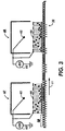
- Figure 2 illustrates the effect of the field lines in the case of an ion source energized by an AC voltage having a DC grid bias 66 voltage intermediate to the image and non image areas of the latent image, represented by (+) and (-) signs, respectively, on the back side of the imaging member 10.
- positive ions flow from the ion source 60 in the direction of the field lines while negative ions (electrons) flow in a direction opposite to the direction of the field lines such that the positive ions presented in the vicinity of a positively charged area of the latent image are repelled from the toner layer 58 while the positive ions in the vicinity of a negatively charged area of the latent image are attracted to the toner layer, and captured thereby.
- a charged toner layer is situated on a latent image bearing imaging member, wherein the charged toner layer is exposed to charged ions for selectively reversing the preexisting charge of the toner layer.
- fringe fields illustrated as field lines extending between image and non-image regions of the latent image can affect the uniformity of the charged toner cake. While the existence of these fringe fields may be advantageous if the fringe fields can be properly controlled, these fringe fields may manifest themselves as image quality defects in the final output document.
- the present invention contemplates an alternative embodiment to the image-wise toner layer charging process described hereinabove, wherein the fringe field effect may be eliminated.
- the image-wise toner charging process of the present invention may be carried out using a neutrally charged toner cake layer coated on the imaging member.
- an ion source or multiple ion sources, must be provided for presenting both negative and positive polarity ions to the toner layer in the vicinity of the latent image for oppositely charging regions of the toner layer corresponding to image and non image areas of the latent image.
- an AC driven scorotron device can be used to provide ions of opposite polarity.
- independent ion sources capable of providing opposite polarity ions can be used.
- independent broad source ion generating devices as variously known in the art may be incorporated, either as a single AC driven device capable of providing both positive and negative charge ions, or as a pair of DC driven devices for providing the same.
- negative ions generated by ion source 68 are absorbed or captured by the neutral toner particles adjacent positively charged areas of the latent image, while negative ions in the vicinity of a negatively charged areas of the latent image are repelled by the latent image.
- the free flowing ions generated by ion sources 67 and 68 are selectively captured by toner layer 58 in accordance with the charge of the latent image areas on the imaging member. This process induces image-wise charging of the toner layer 58, creating a secondary latent image within toner layer 58 made up of image and background areas which are charged oppositely with respect to the charge of the original latent image on the imaging member 10.
- the charge of the original latent image may be converted into the secondary latent image in the toner layer such that the original electrostatic latent image is substantially or completely dissipated into the toner layer after the image-wise toner charging process is complete.
- image separator 20 may be provided in the form of a biased roll member having a surface adjacent to the surface of the imaging member 10 and preferably contacting the toner layer 58 residing on image bearing member 10.
- An electrical biasing source is coupled to the image separator 20 to bias the image separator 20 so as to attract either image or non-image areas of the latent image formed in the toner layer 58 for simultaneously separating and developing the toner layer 58 into image and non-image portions.
- the image separator 20 is biased with a polarity opposite the charge polarity of the image areas in the toner layer 58 for attracting image areas therefrom, thereby producing a developed image made up of selectively separated and transferred portions of the toner cake on the surface of the image separator 20, while leaving background image byproduct on the surface of the imaging member 10.
- the image separator 20 can be provided with an electrical bias having a polarity appropriate for attracting non-image areas away from the imaging member 10, thereby maintaining toner portions corresponding to image areas on the surface of the imaging member, yielding a developed image thereon, while removing non-image or background areas with the image separator 20.
- the developed image may then be transferred to a copy substrate 70 via any means known in the art, which may include an electrostatic transfer apparatus including a corona generating device of the type previously described or a biased transfer roll.
- a pressure transfer system may be employed which may include a heating and/or chemical application device for assisting in the pressure transfer and fixing of the developed image on the output copy substrate 70.
- image transfer can be accomplished via surface energy differentials wherein the surface energy between the image and the member supporting the image prior to transfer is lower than the surface energy between the image and the substrate 70, inducing transfer thereto.
- the image is transferred to a copy substrate via a heated pressure roll, whereby pressure and heat are simultaneously applied to the image to simultaneously transfer and fuse the image to the copy substrate 70.
- a heated pressure roll whereby pressure and heat are simultaneously applied to the image to simultaneously transfer and fuse the image to the copy substrate 70.
- the fusing or so-called fixing system may operate using heat (by any means such as radiation, convection, conduction, induction, etc.), or other known fixation process which may include the introduction of a chemical fixing agent. Since the art of electrostatographic printing is well known, it is noted that several concepts for transfer and/or fusing which could be beneficially used in combination with the image-wise charging system of the present invention have been disclosed in the relevant patent literature.
- the present invention provides a novel image development method and apparatus, whereby image-wise charging is accomplished by a wide beam ion source such that free mobile ions are introduced in the vicinity of an electrostatic latent image coated with layer of developing material.
- the latent image causes the free mobile ions to flow in an image-wise ion stream corresponding to the latent image, which, in turn, leads to image-wise charging of the toner layer, such that the toner layer itself becomes the latent image carrier.
- the latent image carrying toner layer is subsequently developed and transferred to a copy substrate to produce an output document.
Claims (5)
- Abbildungsvorrichtung, enthaltend:ein Abbildungselement (10) zum Ausbilden eines elektrostatischen Latenzbildes auf diesem, wobei das Abbildungselement eine Oberfläche hat, die in der Lage ist, ein Markiermaterial (54) zu tragen;eine Abbildungsvorrichtung (40) zum Erzeugen des elektrostatischen Latenzbildes auf dem Abbildungselement (10), wobei das elektrostatische Latenzbild Abbildungsbereiche enthält, die durch eine erste Ladungsspannung definiert sind, und Nicht-Abbildungsbereiche, die durch eine zweite Ladungsspannung definiert sind, die von der ersten Ladungsspannung unterschieden werden kann;eine Markiermaterial-Zuführvorrichtung (50) zum Abscheiden eines Markiermaterials (54) auf der Oberfläche des Abbildungselementes (10), um eine Markiermaterialschicht (58) darauf benachbart zum elektrostatischen Latenzbild auf dem Abbildungselement (10) auszubilden;eine Ladungsquelle (60) zum wahlweisen Senden von Ladungen zur Markiermaterialschicht (58) in abbildungsartiger Weise in Abhängigkeit des elektrostatischen Latenzbildes auf dem Abbildungselement (10), um ein zweites Latenzbild in der Markiermaterialschicht auszubilden, das Abbildungs- und Nicht-Abbildungsbereiche entsprechend dem elektrostatischen Latenzbild auf dem Abbildungselement (10) hat; undeine Trenneinrichtung (10) zum wahlweisen Trennen von Abschnitten der Markiermaterialschicht (58) in Übereinstimmung mit dem zweiten Latenzbild in der Markiermaterialschicht, um eine entwickelte Abbildung entsprechend dem elektrostatischen Latenzbild zu erzeugen, das auf dem Abbildungselement (10) ausgebildet ist.
- Abbildungsverfahren, enthaltend folgende Schritte:Erzeugen eines elektrostatischen Latenzbildes auf einem Abbildungselement (10), das eine Oberfläche hat, die in der Lage ist, ein Markiermaterial (54) zu tragen, wobei das elektrostatische Latenzbild Abbildungsbereiche enthält, die durch eine erste Ladungsspannung definiert sind, und Nicht-Abbildungsbereiche, die durch eine zweite Ladungsspannung definiert sind, die von der ersten Ladungsspannung unterschieden werden kann;Abscheiden eines Markiermaterials (54) auf der Oberfläche des Abbildungselementes (10), um eine Markiermaterialschicht (58) darauf benachbart der Abbildungs- und Nicht-Abbildungsbereiche des elektrostatischen Latenzbildes auszubilden;wahlweises Senden von Ladungen zur Markiermaterialschicht (58) in abbildungsartiger Weise in Abhängigkeit des elektrostatischen Latenzbildes auf dem Abbildungselement (10) zum Ausbilden eines zweiten Latenzbildes in der Markiermaterialschicht, das Abbildungs- und Nichtabbildungsbereiche entsprechend dem elektrostatischen Latenzbild auf dem Abbildungselement (10) aufweist; undwahlweises Trennen von Abschnitten der Markiermaterialschicht vom Abbildungselement (10) in Übereinstimmung mit dem zweiten Latenzbild in der Markiermaterialschicht zum Erzeugen einer entwickelten Abbildung entsprechend dem elektrostatischen Latenzbild, das auf dem Abbildungselement ausgebildet ist.
- Abbildungsentwicklungsvorrichtung nach Anspruch 1, bei dem die Ladungsquelle (60) eine elektrische Entladung in der Nähe der Schicht (58) des Markiermaterials (54) auf dem Abbildungselement (10) erzeugt, um wahlweise die Schicht (58) des Markiermaterials (54) in Abhängigkeit des elektrostatischen Latenzbildes auf dem Abbildungselement aufzuladen, um so ein zweites elektrostatisches Latenzbild in der Schicht des Markiermaterials (54) zu erzeugen.
- Abbildungsvorrichtung oder Abbildungsverfahren nach einem der vorhergehenden Ansprüche, bei dem das Markiermaterial (54) Tonerpartikel enthält.
- Abbildungsentwicklungsvorrichtung oder Abbildungsverfahren nach einem der vorhergehenden Ansprüche, wobei das zweite elektrostatische Latenzbild Abbildungs- und Nicht-Abbildungsbereiche enthält, die unterscheidbare Ladungspotentiale einer Polarität haben, die den Ladungspotentialen der geladenen Abbildung und den Nicht-Abbildungsbereichen im elektrostatischen Latenzbild entgegengesetzt sind.
Applications Claiming Priority (2)
| Application Number | Priority Date | Filing Date | Title |
|---|---|---|---|
| US08/883,292 US5826147A (en) | 1997-06-27 | 1997-06-27 | Electrostatic latent image development |
| US883292 | 1997-06-27 |
Publications (3)
| Publication Number | Publication Date |
|---|---|
| EP0887714A2 EP0887714A2 (de) | 1998-12-30 |
| EP0887714A3 EP0887714A3 (de) | 1999-08-25 |
| EP0887714B1 true EP0887714B1 (de) | 2003-12-03 |
Family
ID=25382336
Family Applications (1)
| Application Number | Title | Priority Date | Filing Date |
|---|---|---|---|
| EP98304855A Expired - Lifetime EP0887714B1 (de) | 1997-06-27 | 1998-06-19 | Elektrostatische Bildentwicklung |
Country Status (4)
| Country | Link |
|---|---|
| US (1) | US5826147A (de) |
| EP (1) | EP0887714B1 (de) |
| JP (1) | JPH1124378A (de) |
| DE (1) | DE69820160T2 (de) |
Families Citing this family (49)
| Publication number | Priority date | Publication date | Assignee | Title |
|---|---|---|---|---|
| US5966570A (en) * | 1998-01-08 | 1999-10-12 | Xerox Corporation | Image-wise toner layer charging for image development |
| US6115576A (en) * | 1998-05-01 | 2000-09-05 | Ricoh Company, Ltd. | Image forming apparatus using a developing liquid and including an intermediate transfer body |
| DE19823468C1 (de) * | 1998-05-26 | 1999-10-28 | Windmoeller & Hoelscher | Digitale Flexodruckmaschine |
| US6023600A (en) * | 1998-08-31 | 2000-02-08 | Xerox Corporation | Ion charging developement system |
| US5991582A (en) * | 1998-11-02 | 1999-11-23 | Xerox Corporation | Method and apparatus for developing high quality images in a liquid immersion development machine |
| US6006061A (en) * | 1998-11-02 | 1999-12-21 | Xerox Corporation | Method and apparatus for forming high quality images in an electrostatic printing machine |
| US6052550A (en) * | 1998-11-13 | 2000-04-18 | Xerox Corporation | Image separator having conformable layer for contact electrostatic printing |
| US5937248A (en) * | 1998-11-23 | 1999-08-10 | Xerox Corporation | Contact electrostatic printing image forming method and apparatus using image area centered patch of tonerpatches of toner |
| US5991577A (en) * | 1998-11-23 | 1999-11-23 | Xerox Corporation | Air breakdown charge and development image forming method and apparatus using image area centered patches of toner |
| US5991578A (en) * | 1998-11-23 | 1999-11-23 | Xerox Corporation | Image forming reverse charge printing method and apparatus using image area centered patches of toner |
| US5987283A (en) * | 1999-01-19 | 1999-11-16 | Xerox Corporation | Apparatus and method for developing an electrostatic latent image directly from an imaging member to a final substrate |
| US6408154B1 (en) * | 1999-07-06 | 2002-06-18 | Richard Allen Fotland | Method and apparatus for enhancing electrostatic images |
| US6195520B1 (en) | 1999-09-28 | 2001-02-27 | Xerox Corporation | Method and apparatus for forming a uniform layer of liquid developer |
| US6289191B1 (en) * | 1999-11-26 | 2001-09-11 | Xerox Corporation | Single pass, multicolor contact electrostatic printing system |
| US6233420B1 (en) | 1999-11-29 | 2001-05-15 | Xerox Corporation | System and method for enhancing latent image development |
| US6181901B1 (en) * | 1999-11-29 | 2001-01-30 | Xerox Corporation | Multicolor image-on-image forming machine using reverse charge printing (RCP) process |
| US6122471A (en) * | 1999-12-08 | 2000-09-19 | Xerox Corporation | Method and apparatus for delivery of high solids content toner cake in a contact electrostatic printing system |
| US6218066B1 (en) | 2000-01-27 | 2001-04-17 | Xerox Corporation | Developer compositions and processes |
| US6187499B1 (en) * | 2000-01-27 | 2001-02-13 | Xerox Corporation | Imaging apparatus |
| US6180308B1 (en) | 2000-01-27 | 2001-01-30 | Xerox Corporation | Developer compositions and processes |
| US6212347B1 (en) | 2000-01-27 | 2001-04-03 | Xerox Corporation | Imaging apparatuses and processes thereof containing a marking material with a charge acceptance additive of an aluminum complex |
| US6815136B1 (en) | 2000-02-28 | 2004-11-09 | Xerox Corporation | Liquid developers and processes thereof |
| US6256468B1 (en) | 2000-03-13 | 2001-07-03 | Xerox Corporation | Toner cake delivery system having a carrier fluid separation surface |
| US6219501B1 (en) | 2000-03-28 | 2001-04-17 | Xerox Corporation | Method and apparatus for toner cake delivery |
| US6311035B1 (en) | 2000-06-16 | 2001-10-30 | Xerox Corporation | Reprographic system operable for direct transfer of a developed image from an imaging member to a copy substrate |
| US6203961B1 (en) | 2000-06-26 | 2001-03-20 | Xerox Corporation | Developer compositions and processes |
| US6349190B1 (en) * | 2000-09-20 | 2002-02-19 | Xerox Corporation | Low cost process multicolor image reproduction machine |
| US6335136B1 (en) | 2001-02-06 | 2002-01-01 | Xerox Corporation | Developer compositions and processes |
| US6372402B1 (en) | 2001-02-06 | 2002-04-16 | Xerox Corporation | Developer compositions and processes |
| US6458500B1 (en) | 2001-02-06 | 2002-10-01 | Xerox Corporation | Imaging apparatus |
| US6348292B1 (en) | 2001-02-06 | 2002-02-19 | Xerox Corporation | Developer compositions and processes |
| US6346357B1 (en) | 2001-02-06 | 2002-02-12 | Xerox Corporation | Developer compositions and processes |
| US6440629B1 (en) | 2001-02-06 | 2002-08-27 | Xerox Corporation | Imaging apparatus |
| US6536876B1 (en) | 2002-04-15 | 2003-03-25 | Hewlett-Packard Company | Imaging systems and methods |
| JP2005173358A (ja) * | 2003-12-12 | 2005-06-30 | Ricoh Co Ltd | 定着方法、定着装置、及び画像形成装置 |
| US20050250039A1 (en) * | 2004-05-05 | 2005-11-10 | Xerox Corporation | Overprint compositions for xerographic prinits |
| US7166406B2 (en) * | 2004-05-05 | 2007-01-23 | Xerox Corporation | Prevention or reduction of thermal cracking on toner-based prints |
| US7702247B1 (en) | 2005-03-04 | 2010-04-20 | John Michael Weldon | Latent image developer system and method |
| US7521165B2 (en) * | 2006-04-05 | 2009-04-21 | Xerox Corporation | Varnish |
| US7939176B2 (en) | 2005-12-23 | 2011-05-10 | Xerox Corporation | Coated substrates and method of coating |
| US7462401B2 (en) * | 2005-12-23 | 2008-12-09 | Xerox Corporation | Radiation curable composition |
| US7760217B1 (en) | 2006-04-28 | 2010-07-20 | Hewlett-Packard Development Company, L.P. | Imaging methods and imaging devices |
| US20080057433A1 (en) * | 2006-08-30 | 2008-03-06 | Xerox Corporation | Adhesive primer |
| US20080192105A1 (en) * | 2007-02-13 | 2008-08-14 | Xerox Corporation | Digital printing apparatus fittable in a flexographic printing system |
| JP4771484B2 (ja) * | 2007-05-07 | 2011-09-14 | 有限会社 福岡テクノ研工業 | 画像形成方法及び画像形成装置 |
| JP5255369B2 (ja) | 2007-09-25 | 2013-08-07 | 富士フイルム株式会社 | 光硬化性コーティング組成物、オーバープリント及びその製造方法 |
| US8067142B2 (en) | 2007-12-20 | 2011-11-29 | Xerox Corporation | Coating, system and method for conditioning prints |
| US7970333B2 (en) | 2008-07-24 | 2011-06-28 | Xerox Corporation | System and method for protecting an image on a substrate |
| US8833254B2 (en) * | 2012-07-12 | 2014-09-16 | Xerox Corporation | Imaging system with electrophotographic patterning of an image definition material and methods therefor |
Family Cites Families (13)
| Publication number | Priority date | Publication date | Assignee | Title |
|---|---|---|---|---|
| GB1336312A (en) * | 1969-11-14 | 1973-11-07 | Rank Xerox Ltd | Electrophotographic apparatus and process |
| US4504138A (en) * | 1981-10-27 | 1985-03-12 | Coulter Systems Corporation | Method and apparatus for developing electrostatic latent images |
| JPS6095471A (ja) * | 1983-10-28 | 1985-05-28 | Ricoh Co Ltd | 転写装置 |
| JPS6118972A (ja) * | 1984-07-05 | 1986-01-27 | Konishiroku Photo Ind Co Ltd | 光導電性トナ−を用いる記録方法 |
| JPS61251867A (ja) * | 1985-05-01 | 1986-11-08 | Ricoh Co Ltd | 画像形成方法 |
| US5132199A (en) * | 1989-07-31 | 1992-07-21 | Mita Industrial Co., Ltd. | Electrophotographic image-forming method |
| JPH03111719A (ja) * | 1989-09-26 | 1991-05-13 | Seiko Epson Corp | 湿式画像形成方法および湿式画像形成装置 |
| US5387760A (en) * | 1990-10-19 | 1995-02-07 | Seiko Epson Corporation | Wet recording apparatus for developing electrostatic latent image |
| JP2979352B2 (ja) * | 1991-05-30 | 1999-11-15 | コニカ株式会社 | 画像形成方法 |
| JP3524089B2 (ja) * | 1991-07-09 | 2004-04-26 | ヒューレット−パッカード・インデイゴ・ビー・ブイ | 像形成装置および像形成方法 |
| US5351113A (en) * | 1994-01-10 | 1994-09-27 | Xerox Corporation | Pre-pretransfer treatment to increase transfer latitude in tri-level xerography |
| US5619313A (en) * | 1995-05-01 | 1997-04-08 | Xerox Corporation | Method and apparatus for liquid image development and transfer |
| US5937243A (en) * | 1997-06-27 | 1999-08-10 | Xerox Corporation | Image-wise toner layer charging via air breakdown for image development |
-
1997
- 1997-06-27 US US08/883,292 patent/US5826147A/en not_active Expired - Lifetime
-
1998
- 1998-06-19 JP JP10172733A patent/JPH1124378A/ja not_active Withdrawn
- 1998-06-19 EP EP98304855A patent/EP0887714B1/de not_active Expired - Lifetime
- 1998-06-19 DE DE69820160T patent/DE69820160T2/de not_active Expired - Fee Related
Also Published As
| Publication number | Publication date |
|---|---|
| EP0887714A2 (de) | 1998-12-30 |
| DE69820160T2 (de) | 2004-09-09 |
| DE69820160D1 (de) | 2004-01-15 |
| JPH1124378A (ja) | 1999-01-29 |
| EP0887714A3 (de) | 1999-08-25 |
| US5826147A (en) | 1998-10-20 |
Similar Documents
| Publication | Publication Date | Title |
|---|---|---|
| EP0887714B1 (de) | Elektrostatische Bildentwicklung | |
| US5966570A (en) | Image-wise toner layer charging for image development | |
| EP0249385A2 (de) | Zwischenübertragungsgerät | |
| JPH0664397B2 (ja) | 像形成装置及び像形成方法 | |
| EP0887716B1 (de) | Entwicklung eines latenten elektrostatischen Bildes | |
| US5937248A (en) | Contact electrostatic printing image forming method and apparatus using image area centered patch of tonerpatches of toner | |
| US5987283A (en) | Apparatus and method for developing an electrostatic latent image directly from an imaging member to a final substrate | |
| US6122471A (en) | Method and apparatus for delivery of high solids content toner cake in a contact electrostatic printing system | |
| US6006061A (en) | Method and apparatus for forming high quality images in an electrostatic printing machine | |
| US6185399B1 (en) | Multicolor image-on-image forming machine using air breakdown charge and development (ABCD) Process | |
| US5991582A (en) | Method and apparatus for developing high quality images in a liquid immersion development machine | |
| US4761668A (en) | Highlight color printer | |
| US5991577A (en) | Air breakdown charge and development image forming method and apparatus using image area centered patches of toner | |
| US5832352A (en) | Method and apparatus for increasing the mechanical strength of intermediate images for liquid development image conditioning | |
| US5991578A (en) | Image forming reverse charge printing method and apparatus using image area centered patches of toner | |
| US6181901B1 (en) | Multicolor image-on-image forming machine using reverse charge printing (RCP) process | |
| US6020099A (en) | Method and apparatus for forming and refining toner images in an electrostatic printing machine | |
| US4768060A (en) | Push-pull liquid development method and apparatus | |
| US6775499B2 (en) | System and method for contact electrostatic printing | |
| EP1359473B1 (de) | Elektrodynamisches Tonerübertragungssystem | |
| JPH08211687A (ja) | 後段現像部材によるエッジ不揃い及び背景除去 | |
| US3784299A (en) | Dark decay retardation | |
| US6233420B1 (en) | System and method for enhancing latent image development | |
| US5420672A (en) | Concept for prevention of scavengeless nip wire contamination with toner | |
| JPH0510673B2 (de) |
Legal Events
| Date | Code | Title | Description |
|---|---|---|---|
| PUAI | Public reference made under article 153(3) epc to a published international application that has entered the european phase |
Free format text: ORIGINAL CODE: 0009012 |
|
| AK | Designated contracting states |
Kind code of ref document: A2 Designated state(s): DE FR GB |
|
| AX | Request for extension of the european patent |
Free format text: AL;LT;LV;MK;RO;SI |
|
| PUAL | Search report despatched |
Free format text: ORIGINAL CODE: 0009013 |
|
| AK | Designated contracting states |
Kind code of ref document: A3 Designated state(s): AT BE CH CY DE DK ES FI FR GB GR IE IT LI LU MC NL PT SE |
|
| AX | Request for extension of the european patent |
Free format text: AL;LT;LV;MK;RO;SI |
|
| RIC1 | Information provided on ipc code assigned before grant |
Free format text: 6G 03G 15/08 A, 6G 03G 13/08 B, 6G 03G 15/34 B |
|
| 17P | Request for examination filed |
Effective date: 20000225 |
|
| AKX | Designation fees paid |
Free format text: DE FR GB |
|
| 17Q | First examination report despatched |
Effective date: 20020715 |
|
| GRAH | Despatch of communication of intention to grant a patent |
Free format text: ORIGINAL CODE: EPIDOS IGRA |
|
| GRAS | Grant fee paid |
Free format text: ORIGINAL CODE: EPIDOSNIGR3 |
|
| GRAA | (expected) grant |
Free format text: ORIGINAL CODE: 0009210 |
|
| AK | Designated contracting states |
Kind code of ref document: B1 Designated state(s): DE FR GB |
|
| REG | Reference to a national code |
Ref country code: GB Ref legal event code: FG4D |
|
| REF | Corresponds to: |
Ref document number: 69820160 Country of ref document: DE Date of ref document: 20040115 Kind code of ref document: P |
|
| ET | Fr: translation filed | ||
| PLBE | No opposition filed within time limit |
Free format text: ORIGINAL CODE: 0009261 |
|
| STAA | Information on the status of an ep patent application or granted ep patent |
Free format text: STATUS: NO OPPOSITION FILED WITHIN TIME LIMIT |
|
| 26N | No opposition filed |
Effective date: 20040906 |
|
| REG | Reference to a national code |
Ref country code: GB Ref legal event code: 746 Effective date: 20050404 |
|
| PGFP | Annual fee paid to national office [announced via postgrant information from national office to epo] |
Ref country code: FR Payment date: 20060608 Year of fee payment: 9 |
|
| PGFP | Annual fee paid to national office [announced via postgrant information from national office to epo] |
Ref country code: GB Payment date: 20060614 Year of fee payment: 9 |
|
| PGFP | Annual fee paid to national office [announced via postgrant information from national office to epo] |
Ref country code: DE Payment date: 20060615 Year of fee payment: 9 |
|
| GBPC | Gb: european patent ceased through non-payment of renewal fee |
Effective date: 20070619 |
|
| REG | Reference to a national code |
Ref country code: FR Ref legal event code: ST Effective date: 20080229 |
|
| PG25 | Lapsed in a contracting state [announced via postgrant information from national office to epo] |
Ref country code: DE Free format text: LAPSE BECAUSE OF NON-PAYMENT OF DUE FEES Effective date: 20080101 |
|
| PG25 | Lapsed in a contracting state [announced via postgrant information from national office to epo] |
Ref country code: GB Free format text: LAPSE BECAUSE OF NON-PAYMENT OF DUE FEES Effective date: 20070619 |
|
| PG25 | Lapsed in a contracting state [announced via postgrant information from national office to epo] |
Ref country code: FR Free format text: LAPSE BECAUSE OF NON-PAYMENT OF DUE FEES Effective date: 20070702 |