EP0886295A2 - Front panel for plasma display - Google Patents
Front panel for plasma display Download PDFInfo
- Publication number
- EP0886295A2 EP0886295A2 EP98304818A EP98304818A EP0886295A2 EP 0886295 A2 EP0886295 A2 EP 0886295A2 EP 98304818 A EP98304818 A EP 98304818A EP 98304818 A EP98304818 A EP 98304818A EP 0886295 A2 EP0886295 A2 EP 0886295A2
- Authority
- EP
- European Patent Office
- Prior art keywords
- electroconductive
- film
- transparent
- layer
- transparent substrate
- Prior art date
- Legal status (The legal status is an assumption and is not a legal conclusion. Google has not performed a legal analysis and makes no representation as to the accuracy of the status listed.)
- Granted
Links
- 239000012789 electroconductive film Substances 0.000 claims abstract description 80
- 239000000758 substrate Substances 0.000 claims abstract description 74
- 238000000034 method Methods 0.000 claims abstract description 19
- 229920006254 polymer film Polymers 0.000 claims abstract description 11
- 230000005670 electromagnetic radiation Effects 0.000 claims 1
- 239000010410 layer Substances 0.000 description 123
- 239000010408 film Substances 0.000 description 59
- -1 phosphorus compound Chemical class 0.000 description 24
- 229910052751 metal Inorganic materials 0.000 description 21
- 239000002184 metal Substances 0.000 description 21
- 239000000853 adhesive Substances 0.000 description 17
- 230000001070 adhesive effect Effects 0.000 description 17
- 239000011347 resin Substances 0.000 description 17
- 229920005989 resin Polymers 0.000 description 17
- 239000000178 monomer Substances 0.000 description 12
- 150000001875 compounds Chemical class 0.000 description 11
- 239000003795 chemical substances by application Substances 0.000 description 9
- 238000002834 transmittance Methods 0.000 description 8
- 238000011156 evaluation Methods 0.000 description 7
- XEKOWRVHYACXOJ-UHFFFAOYSA-N Ethyl acetate Chemical compound CCOC(C)=O XEKOWRVHYACXOJ-UHFFFAOYSA-N 0.000 description 6
- CERQOIWHTDAKMF-UHFFFAOYSA-N Methacrylic acid Chemical compound CC(=C)C(O)=O CERQOIWHTDAKMF-UHFFFAOYSA-N 0.000 description 6
- VYPSYNLAJGMNEJ-UHFFFAOYSA-N Silicium dioxide Chemical compound O=[Si]=O VYPSYNLAJGMNEJ-UHFFFAOYSA-N 0.000 description 5
- BQCADISMDOOEFD-UHFFFAOYSA-N Silver Chemical compound [Ag] BQCADISMDOOEFD-UHFFFAOYSA-N 0.000 description 5
- 230000000052 comparative effect Effects 0.000 description 5
- 150000002148 esters Chemical class 0.000 description 5
- 238000004519 manufacturing process Methods 0.000 description 5
- 239000012046 mixed solvent Substances 0.000 description 5
- 229910052814 silicon oxide Inorganic materials 0.000 description 5
- 229910052709 silver Inorganic materials 0.000 description 5
- 239000004332 silver Substances 0.000 description 5
- 239000000126 substance Substances 0.000 description 5
- XLOMVQKBTHCTTD-UHFFFAOYSA-N Zinc monoxide Chemical compound [Zn]=O XLOMVQKBTHCTTD-UHFFFAOYSA-N 0.000 description 4
- 238000000576 coating method Methods 0.000 description 4
- 238000001723 curing Methods 0.000 description 4
- 239000011574 phosphorus Substances 0.000 description 4
- 229910052698 phosphorus Inorganic materials 0.000 description 4
- 229920000139 polyethylene terephthalate Polymers 0.000 description 4
- 239000005020 polyethylene terephthalate Substances 0.000 description 4
- 239000004800 polyvinyl chloride Substances 0.000 description 4
- 229920000915 polyvinyl chloride Polymers 0.000 description 4
- 239000011342 resin composition Substances 0.000 description 4
- 238000001771 vacuum deposition Methods 0.000 description 4
- 239000004925 Acrylic resin Substances 0.000 description 3
- 229920000178 Acrylic resin Polymers 0.000 description 3
- RYGMFSIKBFXOCR-UHFFFAOYSA-N Copper Chemical compound [Cu] RYGMFSIKBFXOCR-UHFFFAOYSA-N 0.000 description 3
- LYCAIKOWRPUZTN-UHFFFAOYSA-N Ethylene glycol Chemical compound OCCO LYCAIKOWRPUZTN-UHFFFAOYSA-N 0.000 description 3
- YCKRFDGAMUMZLT-UHFFFAOYSA-N Fluorine atom Chemical compound [F] YCKRFDGAMUMZLT-UHFFFAOYSA-N 0.000 description 3
- PEDCQBHIVMGVHV-UHFFFAOYSA-N Glycerine Chemical compound OCC(O)CO PEDCQBHIVMGVHV-UHFFFAOYSA-N 0.000 description 3
- OAICVXFJPJFONN-UHFFFAOYSA-N Phosphorus Chemical compound [P] OAICVXFJPJFONN-UHFFFAOYSA-N 0.000 description 3
- 239000002202 Polyethylene glycol Substances 0.000 description 3
- 239000004820 Pressure-sensitive adhesive Substances 0.000 description 3
- DNIAPMSPPWPWGF-UHFFFAOYSA-N Propylene glycol Chemical compound CC(O)CO DNIAPMSPPWPWGF-UHFFFAOYSA-N 0.000 description 3
- XUIMIQQOPSSXEZ-UHFFFAOYSA-N Silicon Chemical compound [Si] XUIMIQQOPSSXEZ-UHFFFAOYSA-N 0.000 description 3
- 229920002678 cellulose Polymers 0.000 description 3
- 239000001913 cellulose Substances 0.000 description 3
- 229910052802 copper Inorganic materials 0.000 description 3
- 239000010949 copper Substances 0.000 description 3
- MTHSVFCYNBDYFN-UHFFFAOYSA-N diethylene glycol Chemical compound OCCOCCO MTHSVFCYNBDYFN-UHFFFAOYSA-N 0.000 description 3
- 229920001971 elastomer Polymers 0.000 description 3
- 239000011737 fluorine Substances 0.000 description 3
- 229910052731 fluorine Inorganic materials 0.000 description 3
- 125000002887 hydroxy group Chemical group [H]O* 0.000 description 3
- 229910044991 metal oxide Inorganic materials 0.000 description 3
- 150000004706 metal oxides Chemical class 0.000 description 3
- TWNQGVIAIRXVLR-UHFFFAOYSA-N oxo(oxoalumanyloxy)alumane Chemical compound O=[Al]O[Al]=O TWNQGVIAIRXVLR-UHFFFAOYSA-N 0.000 description 3
- 230000000149 penetrating effect Effects 0.000 description 3
- 229920001223 polyethylene glycol Polymers 0.000 description 3
- 238000006116 polymerization reaction Methods 0.000 description 3
- 239000010703 silicon Substances 0.000 description 3
- 229910052710 silicon Inorganic materials 0.000 description 3
- 150000005846 sugar alcohols Polymers 0.000 description 3
- 229910001928 zirconium oxide Inorganic materials 0.000 description 3
- POAOYUHQDCAZBD-UHFFFAOYSA-N 2-butoxyethanol Chemical compound CCCCOCCO POAOYUHQDCAZBD-UHFFFAOYSA-N 0.000 description 2
- 229920002284 Cellulose triacetate Polymers 0.000 description 2
- 239000005749 Copper compound Substances 0.000 description 2
- 239000004593 Epoxy Substances 0.000 description 2
- LFQSCWFLJHTTHZ-UHFFFAOYSA-N Ethanol Chemical compound CCO LFQSCWFLJHTTHZ-UHFFFAOYSA-N 0.000 description 2
- VZCYOOQTPOCHFL-OWOJBTEDSA-N Fumaric acid Chemical compound OC(=O)\C=C\C(O)=O VZCYOOQTPOCHFL-OWOJBTEDSA-N 0.000 description 2
- 229920000877 Melamine resin Polymers 0.000 description 2
- PXHVJJICTQNCMI-UHFFFAOYSA-N Nickel Chemical compound [Ni] PXHVJJICTQNCMI-UHFFFAOYSA-N 0.000 description 2
- CTQNGGLPUBDAKN-UHFFFAOYSA-N O-Xylene Chemical compound CC1=CC=CC=C1C CTQNGGLPUBDAKN-UHFFFAOYSA-N 0.000 description 2
- KDLHZDBZIXYQEI-UHFFFAOYSA-N Palladium Chemical compound [Pd] KDLHZDBZIXYQEI-UHFFFAOYSA-N 0.000 description 2
- 239000004743 Polypropylene Substances 0.000 description 2
- GWEVSGVZZGPLCZ-UHFFFAOYSA-N Titan oxide Chemical compound O=[Ti]=O GWEVSGVZZGPLCZ-UHFFFAOYSA-N 0.000 description 2
- NNLVGZFZQQXQNW-ADJNRHBOSA-N [(2r,3r,4s,5r,6s)-4,5-diacetyloxy-3-[(2s,3r,4s,5r,6r)-3,4,5-triacetyloxy-6-(acetyloxymethyl)oxan-2-yl]oxy-6-[(2r,3r,4s,5r,6s)-4,5,6-triacetyloxy-2-(acetyloxymethyl)oxan-3-yl]oxyoxan-2-yl]methyl acetate Chemical compound O([C@@H]1O[C@@H]([C@H]([C@H](OC(C)=O)[C@H]1OC(C)=O)O[C@H]1[C@@H]([C@@H](OC(C)=O)[C@H](OC(C)=O)[C@@H](COC(C)=O)O1)OC(C)=O)COC(=O)C)[C@@H]1[C@@H](COC(C)=O)O[C@@H](OC(C)=O)[C@H](OC(C)=O)[C@H]1OC(C)=O NNLVGZFZQQXQNW-ADJNRHBOSA-N 0.000 description 2
- NIXOWILDQLNWCW-UHFFFAOYSA-N acrylic acid group Chemical group C(C=C)(=O)O NIXOWILDQLNWCW-UHFFFAOYSA-N 0.000 description 2
- 150000001336 alkenes Chemical class 0.000 description 2
- 230000015572 biosynthetic process Effects 0.000 description 2
- 150000001732 carboxylic acid derivatives Chemical class 0.000 description 2
- 229920001577 copolymer Polymers 0.000 description 2
- YEOCHZFPBYUXMC-UHFFFAOYSA-L copper benzoate Chemical compound [Cu+2].[O-]C(=O)C1=CC=CC=C1.[O-]C(=O)C1=CC=CC=C1 YEOCHZFPBYUXMC-UHFFFAOYSA-L 0.000 description 2
- 150000001880 copper compounds Chemical class 0.000 description 2
- 238000005336 cracking Methods 0.000 description 2
- 150000002009 diols Chemical class 0.000 description 2
- 230000000694 effects Effects 0.000 description 2
- 238000005516 engineering process Methods 0.000 description 2
- 229910003437 indium oxide Inorganic materials 0.000 description 2
- PJXISJQVUVHSOJ-UHFFFAOYSA-N indium(iii) oxide Chemical compound [O-2].[O-2].[O-2].[In+3].[In+3] PJXISJQVUVHSOJ-UHFFFAOYSA-N 0.000 description 2
- 238000007733 ion plating Methods 0.000 description 2
- ORUIBWPALBXDOA-UHFFFAOYSA-L magnesium fluoride Chemical compound [F-].[F-].[Mg+2] ORUIBWPALBXDOA-UHFFFAOYSA-L 0.000 description 2
- 229910001635 magnesium fluoride Inorganic materials 0.000 description 2
- JDSHMPZPIAZGSV-UHFFFAOYSA-N melamine Chemical compound NC1=NC(N)=NC(N)=N1 JDSHMPZPIAZGSV-UHFFFAOYSA-N 0.000 description 2
- 229910001507 metal halide Inorganic materials 0.000 description 2
- 150000005309 metal halides Chemical class 0.000 description 2
- SNVLJLYUUXKWOJ-UHFFFAOYSA-N methylidenecarbene Chemical compound C=[C] SNVLJLYUUXKWOJ-UHFFFAOYSA-N 0.000 description 2
- 238000002156 mixing Methods 0.000 description 2
- JRZJOMJEPLMPRA-UHFFFAOYSA-N olefin Natural products CCCCCCCC=C JRZJOMJEPLMPRA-UHFFFAOYSA-N 0.000 description 2
- BPUBBGLMJRNUCC-UHFFFAOYSA-N oxygen(2-);tantalum(5+) Chemical compound [O-2].[O-2].[O-2].[O-2].[O-2].[Ta+5].[Ta+5] BPUBBGLMJRNUCC-UHFFFAOYSA-N 0.000 description 2
- RVTZCBVAJQQJTK-UHFFFAOYSA-N oxygen(2-);zirconium(4+) Chemical compound [O-2].[O-2].[Zr+4] RVTZCBVAJQQJTK-UHFFFAOYSA-N 0.000 description 2
- XNGIFLGASWRNHJ-UHFFFAOYSA-N phthalic acid Chemical compound OC(=O)C1=CC=CC=C1C(O)=O XNGIFLGASWRNHJ-UHFFFAOYSA-N 0.000 description 2
- BASFCYQUMIYNBI-UHFFFAOYSA-N platinum Chemical compound [Pt] BASFCYQUMIYNBI-UHFFFAOYSA-N 0.000 description 2
- 229920003229 poly(methyl methacrylate) Polymers 0.000 description 2
- 239000004417 polycarbonate Substances 0.000 description 2
- 229920000515 polycarbonate Polymers 0.000 description 2
- 229920005668 polycarbonate resin Polymers 0.000 description 2
- 239000004431 polycarbonate resin Substances 0.000 description 2
- 239000005056 polyisocyanate Substances 0.000 description 2
- 229920001228 polyisocyanate Polymers 0.000 description 2
- 239000004926 polymethyl methacrylate Substances 0.000 description 2
- 229920000306 polymethylpentene Polymers 0.000 description 2
- 239000011116 polymethylpentene Substances 0.000 description 2
- 229920001155 polypropylene Polymers 0.000 description 2
- 239000007787 solid Substances 0.000 description 2
- 239000002904 solvent Substances 0.000 description 2
- 238000004544 sputter deposition Methods 0.000 description 2
- 229910001936 tantalum oxide Inorganic materials 0.000 description 2
- XOLBLPGZBRYERU-UHFFFAOYSA-N tin dioxide Chemical compound O=[Sn]=O XOLBLPGZBRYERU-UHFFFAOYSA-N 0.000 description 2
- 229910001887 tin oxide Inorganic materials 0.000 description 2
- OGIDPMRJRNCKJF-UHFFFAOYSA-N titanium oxide Inorganic materials [Ti]=O OGIDPMRJRNCKJF-UHFFFAOYSA-N 0.000 description 2
- VZCYOOQTPOCHFL-UHFFFAOYSA-N trans-butenedioic acid Natural products OC(=O)C=CC(O)=O VZCYOOQTPOCHFL-UHFFFAOYSA-N 0.000 description 2
- 239000008096 xylene Substances 0.000 description 2
- 239000011787 zinc oxide Substances 0.000 description 2
- FVQMJJQUGGVLEP-UHFFFAOYSA-N (2-methylpropan-2-yl)oxy 2-ethylhexaneperoxoate Chemical compound CCCCC(CC)C(=O)OOOC(C)(C)C FVQMJJQUGGVLEP-UHFFFAOYSA-N 0.000 description 1
- JAHNSTQSQJOJLO-UHFFFAOYSA-N 2-(3-fluorophenyl)-1h-imidazole Chemical compound FC1=CC=CC(C=2NC=CN=2)=C1 JAHNSTQSQJOJLO-UHFFFAOYSA-N 0.000 description 1
- RWLALWYNXFYRGW-UHFFFAOYSA-N 2-Ethyl-1,3-hexanediol Chemical compound CCCC(O)C(CC)CO RWLALWYNXFYRGW-UHFFFAOYSA-N 0.000 description 1
- TXBCBTDQIULDIA-UHFFFAOYSA-N 2-[[3-hydroxy-2,2-bis(hydroxymethyl)propoxy]methyl]-2-(hydroxymethyl)propane-1,3-diol Chemical compound OCC(CO)(CO)COCC(CO)(CO)CO TXBCBTDQIULDIA-UHFFFAOYSA-N 0.000 description 1
- OMIGHNLMNHATMP-UHFFFAOYSA-N 2-hydroxyethyl prop-2-enoate Chemical group OCCOC(=O)C=C OMIGHNLMNHATMP-UHFFFAOYSA-N 0.000 description 1
- GWZMWHWAWHPNHN-UHFFFAOYSA-N 2-hydroxypropyl prop-2-enoate Chemical group CC(O)COC(=O)C=C GWZMWHWAWHPNHN-UHFFFAOYSA-N 0.000 description 1
- 229920002799 BoPET Polymers 0.000 description 1
- VYZAMTAEIAYCRO-UHFFFAOYSA-N Chromium Chemical compound [Cr] VYZAMTAEIAYCRO-UHFFFAOYSA-N 0.000 description 1
- 239000005057 Hexamethylene diisocyanate Substances 0.000 description 1
- VVQNEPGJFQJSBK-UHFFFAOYSA-N Methyl methacrylate Chemical compound COC(=O)C(C)=C VVQNEPGJFQJSBK-UHFFFAOYSA-N 0.000 description 1
- ZOKXTWBITQBERF-UHFFFAOYSA-N Molybdenum Chemical compound [Mo] ZOKXTWBITQBERF-UHFFFAOYSA-N 0.000 description 1
- XBXFGOSIPGWNLZ-UHFFFAOYSA-N O=C1C=C(CC(C)(C)C1)C.N=C=O Chemical compound O=C1C=C(CC(C)(C)C1)C.N=C=O XBXFGOSIPGWNLZ-UHFFFAOYSA-N 0.000 description 1
- 239000004793 Polystyrene Substances 0.000 description 1
- OFOBLEOULBTSOW-UHFFFAOYSA-N Propanedioic acid Natural products OC(=O)CC(O)=O OFOBLEOULBTSOW-UHFFFAOYSA-N 0.000 description 1
- KDYFGRWQOYBRFD-UHFFFAOYSA-N Succinic acid Natural products OC(=O)CCC(O)=O KDYFGRWQOYBRFD-UHFFFAOYSA-N 0.000 description 1
- RTAQQCXQSZGOHL-UHFFFAOYSA-N Titanium Chemical compound [Ti] RTAQQCXQSZGOHL-UHFFFAOYSA-N 0.000 description 1
- ZJCCRDAZUWHFQH-UHFFFAOYSA-N Trimethylolpropane Chemical compound CCC(CO)(CO)CO ZJCCRDAZUWHFQH-UHFFFAOYSA-N 0.000 description 1
- QCWXUUIWCKQGHC-UHFFFAOYSA-N Zirconium Chemical compound [Zr] QCWXUUIWCKQGHC-UHFFFAOYSA-N 0.000 description 1
- IAXXETNIOYFMLW-COPLHBTASA-N [(1s,3s,4s)-4,7,7-trimethyl-3-bicyclo[2.2.1]heptanyl] 2-methylprop-2-enoate Chemical compound C1C[C@]2(C)[C@@H](OC(=O)C(=C)C)C[C@H]1C2(C)C IAXXETNIOYFMLW-COPLHBTASA-N 0.000 description 1
- YIMQCDZDWXUDCA-UHFFFAOYSA-N [4-(hydroxymethyl)cyclohexyl]methanol Chemical compound OCC1CCC(CO)CC1 YIMQCDZDWXUDCA-UHFFFAOYSA-N 0.000 description 1
- AZWHFTKIBIQKCA-UHFFFAOYSA-N [Sn+2]=O.[O-2].[In+3] Chemical compound [Sn+2]=O.[O-2].[In+3] AZWHFTKIBIQKCA-UHFFFAOYSA-N 0.000 description 1
- 239000012790 adhesive layer Substances 0.000 description 1
- CDQSJQSWAWPGKG-UHFFFAOYSA-N butane-1,1-diol Chemical compound CCCC(O)O CDQSJQSWAWPGKG-UHFFFAOYSA-N 0.000 description 1
- KDYFGRWQOYBRFD-NUQCWPJISA-N butanedioic acid Chemical compound O[14C](=O)CC[14C](O)=O KDYFGRWQOYBRFD-NUQCWPJISA-N 0.000 description 1
- 229910052804 chromium Inorganic materials 0.000 description 1
- 239000011651 chromium Substances 0.000 description 1
- 239000007822 coupling agent Substances 0.000 description 1
- 238000005520 cutting process Methods 0.000 description 1
- IFDVQVHZEKPUSC-UHFFFAOYSA-N cyclohex-3-ene-1,2-dicarboxylic acid Chemical compound OC(=O)C1CCC=CC1C(O)=O IFDVQVHZEKPUSC-UHFFFAOYSA-N 0.000 description 1
- 230000002950 deficient Effects 0.000 description 1
- GPLRAVKSCUXZTP-UHFFFAOYSA-N diglycerol Chemical compound OCC(O)COCC(O)CO GPLRAVKSCUXZTP-UHFFFAOYSA-N 0.000 description 1
- 238000001035 drying Methods 0.000 description 1
- 238000001227 electron beam curing Methods 0.000 description 1
- UHESRSKEBRADOO-UHFFFAOYSA-N ethyl carbamate;prop-2-enoic acid Chemical compound OC(=O)C=C.CCOC(N)=O UHESRSKEBRADOO-UHFFFAOYSA-N 0.000 description 1
- STVZJERGLQHEKB-UHFFFAOYSA-N ethylene glycol dimethacrylate Chemical compound CC(=C)C(=O)OCCOC(=O)C(C)=C STVZJERGLQHEKB-UHFFFAOYSA-N 0.000 description 1
- 230000008020 evaporation Effects 0.000 description 1
- 238000001704 evaporation Methods 0.000 description 1
- 230000001747 exhibiting effect Effects 0.000 description 1
- 239000001530 fumaric acid Substances 0.000 description 1
- 239000011521 glass Substances 0.000 description 1
- PCHJSUWPFVWCPO-UHFFFAOYSA-N gold Chemical compound [Au] PCHJSUWPFVWCPO-UHFFFAOYSA-N 0.000 description 1
- 229910052737 gold Inorganic materials 0.000 description 1
- 239000010931 gold Substances 0.000 description 1
- 238000013007 heat curing Methods 0.000 description 1
- RRAMGCGOFNQTLD-UHFFFAOYSA-N hexamethylene diisocyanate Chemical compound O=C=NCCCCCCN=C=O RRAMGCGOFNQTLD-UHFFFAOYSA-N 0.000 description 1
- ACCCMOQWYVYDOT-UHFFFAOYSA-N hexane-1,1-diol Chemical compound CCCCCC(O)O ACCCMOQWYVYDOT-UHFFFAOYSA-N 0.000 description 1
- 238000007654 immersion Methods 0.000 description 1
- 239000003999 initiator Substances 0.000 description 1
- 229940119545 isobornyl methacrylate Drugs 0.000 description 1
- 239000012948 isocyanate Substances 0.000 description 1
- IQPQWNKOIGAROB-UHFFFAOYSA-N isocyanate group Chemical group [N-]=C=O IQPQWNKOIGAROB-UHFFFAOYSA-N 0.000 description 1
- 150000002513 isocyanates Chemical class 0.000 description 1
- 238000001755 magnetron sputter deposition Methods 0.000 description 1
- VZCYOOQTPOCHFL-UPHRSURJSA-N maleic acid Chemical compound OC(=O)\C=C/C(O)=O VZCYOOQTPOCHFL-UPHRSURJSA-N 0.000 description 1
- 239000011976 maleic acid Substances 0.000 description 1
- 239000000463 material Substances 0.000 description 1
- 150000002739 metals Chemical class 0.000 description 1
- 125000002496 methyl group Chemical group [H]C([H])([H])* 0.000 description 1
- LVHBHZANLOWSRM-UHFFFAOYSA-N methylenebutanedioic acid Natural products OC(=O)CC(=C)C(O)=O LVHBHZANLOWSRM-UHFFFAOYSA-N 0.000 description 1
- 239000000203 mixture Substances 0.000 description 1
- 229910052750 molybdenum Inorganic materials 0.000 description 1
- 239000011733 molybdenum Substances 0.000 description 1
- 238000000465 moulding Methods 0.000 description 1
- SLCVBVWXLSEKPL-UHFFFAOYSA-N neopentyl glycol Chemical compound OCC(C)(C)CO SLCVBVWXLSEKPL-UHFFFAOYSA-N 0.000 description 1
- 229910052759 nickel Inorganic materials 0.000 description 1
- 229910052763 palladium Inorganic materials 0.000 description 1
- WXZMFSXDPGVJKK-UHFFFAOYSA-N pentaerythritol Chemical compound OCC(CO)(CO)CO WXZMFSXDPGVJKK-UHFFFAOYSA-N 0.000 description 1
- UWJJYHHHVWZFEP-UHFFFAOYSA-N pentane-1,1-diol Chemical compound CCCCC(O)O UWJJYHHHVWZFEP-UHFFFAOYSA-N 0.000 description 1
- 229960004624 perflexane Drugs 0.000 description 1
- ZJIJAJXFLBMLCK-UHFFFAOYSA-N perfluorohexane Chemical compound FC(F)(F)C(F)(F)C(F)(F)C(F)(F)C(F)(F)C(F)(F)F ZJIJAJXFLBMLCK-UHFFFAOYSA-N 0.000 description 1
- 125000002467 phosphate group Chemical group [H]OP(=O)(O[H])O[*] 0.000 description 1
- 239000000049 pigment Substances 0.000 description 1
- 229910052697 platinum Inorganic materials 0.000 description 1
- 229920001610 polycaprolactone Polymers 0.000 description 1
- 239000004632 polycaprolactone Substances 0.000 description 1
- 229920001451 polypropylene glycol Polymers 0.000 description 1
- 229920002223 polystyrene Polymers 0.000 description 1
- 229920002635 polyurethane Polymers 0.000 description 1
- 239000004814 polyurethane Substances 0.000 description 1
- ULWHHBHJGPPBCO-UHFFFAOYSA-N propane-1,1-diol Chemical compound CCC(O)O ULWHHBHJGPPBCO-UHFFFAOYSA-N 0.000 description 1
- 239000007870 radical polymerization initiator Substances 0.000 description 1
- 238000004528 spin coating Methods 0.000 description 1
- 229920003002 synthetic resin Polymers 0.000 description 1
- 239000000057 synthetic resin Substances 0.000 description 1
- UFDHBDMSHIXOKF-UHFFFAOYSA-N tetrahydrophthalic acid Natural products OC(=O)C1=C(C(O)=O)CCCC1 UFDHBDMSHIXOKF-UHFFFAOYSA-N 0.000 description 1
- 238000012719 thermal polymerization Methods 0.000 description 1
- YODZTKMDCQEPHD-UHFFFAOYSA-N thiodiglycol Chemical compound OCCSCCO YODZTKMDCQEPHD-UHFFFAOYSA-N 0.000 description 1
- 150000003585 thioureas Chemical class 0.000 description 1
- 229910052719 titanium Inorganic materials 0.000 description 1
- 239000010936 titanium Substances 0.000 description 1
- WFKWXMTUELFFGS-UHFFFAOYSA-N tungsten Chemical compound [W] WFKWXMTUELFFGS-UHFFFAOYSA-N 0.000 description 1
- 229910052721 tungsten Inorganic materials 0.000 description 1
- 239000010937 tungsten Substances 0.000 description 1
Images

Classifications
-
- H—ELECTRICITY
- H05—ELECTRIC TECHNIQUES NOT OTHERWISE PROVIDED FOR
- H05K—PRINTED CIRCUITS; CASINGS OR CONSTRUCTIONAL DETAILS OF ELECTRIC APPARATUS; MANUFACTURE OF ASSEMBLAGES OF ELECTRICAL COMPONENTS
- H05K9/00—Screening of apparatus or components against electric or magnetic fields
- H05K9/0073—Shielding materials
- H05K9/0094—Shielding materials being light-transmitting, e.g. transparent, translucent
- H05K9/0096—Shielding materials being light-transmitting, e.g. transparent, translucent for television displays, e.g. plasma display panel
-
- H—ELECTRICITY
- H01—ELECTRIC ELEMENTS
- H01J—ELECTRIC DISCHARGE TUBES OR DISCHARGE LAMPS
- H01J11/00—Gas-filled discharge tubes with alternating current induction of the discharge, e.g. alternating current plasma display panels [AC-PDP]; Gas-filled discharge tubes without any main electrode inside the vessel; Gas-filled discharge tubes with at least one main electrode outside the vessel
- H01J11/10—AC-PDPs with at least one main electrode being out of contact with the plasma
-
- H—ELECTRICITY
- H01—ELECTRIC ELEMENTS
- H01J—ELECTRIC DISCHARGE TUBES OR DISCHARGE LAMPS
- H01J11/00—Gas-filled discharge tubes with alternating current induction of the discharge, e.g. alternating current plasma display panels [AC-PDP]; Gas-filled discharge tubes without any main electrode inside the vessel; Gas-filled discharge tubes with at least one main electrode outside the vessel
- H01J11/20—Constructional details
- H01J11/34—Vessels, containers or parts thereof, e.g. substrates
- H01J11/44—Optical arrangements or shielding arrangements, e.g. filters, black matrices, light reflecting means or electromagnetic shielding means
-
- H—ELECTRICITY
- H01—ELECTRIC ELEMENTS
- H01J—ELECTRIC DISCHARGE TUBES OR DISCHARGE LAMPS
- H01J2211/00—Plasma display panels with alternate current induction of the discharge, e.g. AC-PDPs
- H01J2211/20—Constructional details
- H01J2211/34—Vessels, containers or parts thereof, e.g. substrates
- H01J2211/44—Optical arrangements or shielding arrangements, e.g. filters or lenses
- H01J2211/446—Electromagnetic shielding means; Antistatic means
Definitions
- the present invention relates to a front panel for a plasma display.
- a plasma display has been drawing special interest as a display which has large surface area and is flat, however, the screen thereof generates an electromagnetic wave which exerts an influence on other apparatuses and, therefore, it is necessary to shield the wave.
- Such a front panel has problems that a large scale vacuum deposition apparatus is required and the production method thereof is complicated since formation of an electroconductive layer by vacuum deposition method and the like is required for each transparent substrate.
- the present inventors have intensively investigated for developing a front panel which can efficiently shield an electromagnetic wave generated from a screen of a plasma display and can be produced in a relatively simple process. As a result, it has been found that such a front panel can be obtained by placing two or more electroconductive films on a transparent substrate.
- the present invention has been accomplished on the basis of the above findings.
- the present invention provides a front panel for a plasma display comprising a transparent substrate and two or more electroconductive films placed on the transparent substrate, thefilmsbeing obtained by placing a transparent electroconductive layer on at least one side of surface of a polymer film.
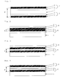
- Figs. 1 to 7 are schematic cross-sectional views of examples of the front panel for a plasma display of the present invention.
- the present invention provides a front panel for a plasma display comprising a transparent substrate and two or more electroconductive films.
- the transparent substrate in the front panel of the present invention preferably comprises a synthetic resin such as an acrylic resin, polycarbonate, polystyrene or methyl methacrylate-styrene copolymer, and the acrylic resin is especially preferred since it can be easily processed into the intended size and has excellent transparency.
- the transparent substrate used has a thickness of usually from about 0.01 mm to about 10 mm, preferably from about 0.5 mm to about 10 mm. Size of the transparent substrate is appropriately determined depending on screen size of the display.
- the transparent substrate may be substantially transparent, and further, may be colored by a dye, pigment and the like.
- Light transmittance at a wavelength in the range of from about 400 nm to about 600 nm is usually about 50% or more, preferably about 60% or more.
- the average light transmittance at a wavelength in the range of from about 850 nm to about 1000 nm is preferably about 10% or less.
- the transparent substrate having the ability to shield a near-infrared ray can be produced, for example, by molding a resin composition comprising a compound containing elemental copper, and a copolymer obtained by copolymerizing a monomer havinganunsaturated double bond and anelemental phosphorus-containing monomer (, which is described in detail, for example, in Japanese Patent Application Laid-Open (JP-A) No. Hei 6-118228), a resin composition comprising a copper compound and a phosphorus compound (, which is described in detail, for example, in Japanese Patent Application Publication (JP-B) No.
- JP-A Japanese Patent Application Laid-Open
- JP-B Japanese Patent Application Publication
- the substrate surface of at least one side on which the electroconductive film is laminated has been subjected to a hard coat treatment, so that when exposed to high temperature generated from the plasma display for long period of time, the electroconductive film is not easily released from the transparent substrate, and in the case in which the transparent substrate comprises an acrylic resin, the effect is remarkable.
- the hard coat layer used in the present invention may be a commonly used one. Examples thereof include layers prepared by polymerization and curing of polyfunctional monomers or oligomers thereof. Examples of the polyfunctional monomer include acryl-based monomers, silicon-based monomers, epoxy-based monomers and melamine-based monomers.
- a hard coat agent such as an acryl-based hard coat agent, silicon-based hard coat agent, epoxy-based hard coat agent or melamine-based hard coat agent, which contains one or more of the above polyfunctional monomers or oligomers thereof as a main component, is applied and then, is polymerized and cured to form a hard coat layer.
- acryl-based monomer for example, a polymerizable compound containing at least two (meth)acryloyloxy groups in the molecule may be listed.
- (meth)acryloyloxy represents both acryloyloxy and methacryloyloxy, and hereinafter, the term “(meth)” has an analogous meaning indicating the optional presence of a methyl substituent.
- the polymerizable compound examples include an ester compound of a polyhydric alcohol with (meth)acrylic acid, a urethane-modified (meth)acrylic oligomer obtained from a compound having an isocyanate group at the end and a (meth)acrylic acid derivative having a hydroxyl group.
- polyhydric alcohol examples include dihydric alcohol such as ethylene glycol, diethylene glycol, polyethylene glycol, propylene glycol, polypropylene glycol, propane diol, butane diol, pentane diol, hexane diol, neopentyl glycol, 2-ethyl-1,3-hexanediol, 2,2'-thiodiethanol and 1,4-cyclohexane dimethanol, and tri- or more hydric alcohol such as trimethylol propane, pentaglycerol, glycerol, pentaerythritol, diglycerol, dipentaglycerol and dipentaerythritol.
- dihydric alcohol such as ethylene glycol, diethylene glycol, polyethylene glycol, propylene glycol, polypropylene glycol, propane diol, butane diol, pentane diol, hexane diol, neopentyl glycol
- a polyvalent unsaturated carboxylic acid may be further added in small amount to prepare a mixed ester for imparting flexibility to the resulting cured film to prevent cracking.
- polyvalent unsaturated carboxylic acid examples include succinic acid, tetrahydro phthalic acid, phthalic acid, maleic acid, fumaric acid and itaconic acid.
- a urethane-modified (meth)acrylic oligomer can be obtained, for example, by reacting a (meth)acrylic acid derivative with an end isocyanate polyurethane obtained by reacting a polyisocyanate with an oligomer having a plurality of hydroxyl group.
- polyisocyanate hexamethylene diisocyanate and isophorone isocyanate may be exemplified; as the oligomer having a plurality of hydroxyl groups, polycaprolactone diol and polytetramethylene diol may be exemplified; and as the (meth)acrylic acid derivative, (meth)acrylic acid hydroxyalkylated compounds such as (meth)acrylic acid-2-hydroxyethyl and (meth)acrylic acid-2-hydroxypropyl may be exemplified.
- the polyfunctional monomer or oligomer thereof is usually, for example, mixed with an initiator and then, is applied on a transparent substrate by a common method such as a spin coating method, immersion coating method, roll-coat coating method, gravure-coat coating method and curtain flow coating method and then, it is polymerized and cured. Further, it may be diluted with various kinds of solvents before being applied, and in this case, the solvent is usually evaporated by the curing after the applying.
- a method such as an ultraviolet ray curing method, heat curing method or electron beam curing method is appropriately conducted depending on the kind of the polyfunctional monomer or oligomer thereof to be used.
- the thickness Of the hard coat layer thus formed on the surface of the transparent substrate is not particularly restricted, and preferably from about 1 ⁇ m to about 20 ⁇ m. When the thickness is less than about 1 ⁇ m , interference stripes derived from the hard coat layer tend to easily occur, and when over about 20 ⁇ m, cracking tends to easily occur on the hard coat layer.
- an adhesive layer may be provided between the transparent substrate and the hard coat layer.
- the electroconductive film is obtained by placing a transparent electroconductive layer on at least one surface of a polymer film.
- the transparent electroconductive layer for example, a layer made of metal and a layer made of one or more metal oxides may be listed.
- Metals such as gold, silver, platinum, palladium, copper, titanium, chromium, molybdenum, nickel and zirconium, and metal oxides such as silicon oxide, titanium oxide, tantalum oxide, tin oxide, indium oxide, zirconium oxide and zinc oxide may be exemplified respectively, and these may be used alone or in combination of two or more.
- silver is preferred since an electroconductive film having excellent electroconductivity is easily obtained with silver.
- the transparent electroconductive layer is a layer made of metal (, which is called “a metal layer” hereinafter,) it is preferred that dielectric layers are placed on both sides of surface of the transparent electroconductive layer since reflection of visible light by the metal layer can be lowered by the dielectric layers.
- a metal layer a layer made of metal
- dielectric layers are placed on both sides of surface of the transparent electroconductive layer since reflection of visible light by the metal layer can be lowered by the dielectric layers.
- Examples of the transparent electroconductive layer in view of structure include the following: (, in the following , "A/B" represents A is followed by B in a layer,)
- the surface resistance of the transparent electroconductive layer is usually 50 ⁇ / ⁇ or less, preferably 10 ⁇ / ⁇ or less, more preferably 6 ⁇ / ⁇ or less for obtaining sufficient electromagnetic wave shielding function.
- the transparent electroconductive layer can be placed on the surface of a polymer film, for example, by a method such as vacuum deposition, sputtering or ion-plating.
- the thickness of the transparent electroconductive layer is usually from about 30 nm to about 1000 nm, preferably from about 50 nm to about 500 nm. When the thickness is less than 30 nm, electroconductivity tends to be insufficient, though it depends on the kind of metal and metal oxide constituting the transparent electroconductive layer. On the other hand, when the thickness is more than 1000 nm, the transparency tends to be deficient, and for example, the tendency is remarkable when silver is used.
- the polymer film, on which the transparent electroconductive layer is formed is not particularly restricted, providing it has transparency, and in view of easy handling, processability and economy, there are usually used an ester-based resin film mainly containing an ester-based resin such as polyethylene terephthalate , an acryl-based resin film mainly containing an acryl-based resin such as polymethyl methacrylate, a cellulose-based resin film mainly containing a cellulose-based resin such as triacetylcellulose, a film mainly containing an olefin-based resin such as polypropylene or polymethylpentene, a polycarbonate-based resin film mainly containing a polycarbonate resin, or a polyvinyl chloride-based resin film mainly containing a polyvinyl chloride resin.
- the thickness of the film is usually from about 20 ⁇ m to about 500 ⁇ m.
- the electroconductive film can be obtained by cutting out of a film which is produced by using a roll film as a raw polymer film and a transparent electroconductive layer having been continuously placed on the polymer film.
- the two or more electroconductive films are placed on the transparent substrate.
- Three or more electroconductive films may be placed, however, two electroconductive films are usually placed in view of cost and procedure of the production process thereof since a desired electromagnetic-wave-shielding property is able to be obtained when two electroconductive films are placed.
- two or more electroconductive films 4 may be placed on at least one side of surface of the transparent substrate 1, or as shown in Fig. 1, the films 4 may be placed on both sides of surface of the transparent substrate 1.
- an adhesive may be used effectively.
- the adhesive for example, an acryl-based adhesive and a rubber-based adhesive may be listed.
- the adhesive is applied on one side of surface of an electroconductive film, then, the electroconductive film is placed on a transparent substrate, then, they are press-bonded, for example using a roll press-bonding pasting machine or batch-wise pasting machine.
- the adhesive may advantageously be applied to the surface of the electroconductive film on the side opposite to the side on which the transparent electroconductive layer is placed.
- outward and inward mean “outward relative to the transparent substrate” and “inward relative to the transparent substrate” respectively.
- an electroconductive film 4 may be placed on a transparent substrate 1 so that the transparent electroconductive layer 3 faces outward, and onto this may be placed another electroconductive film 4 so that the transparent electroconductive layer 3 faces inward, or as shown in Fig. 3, an electroconductive film 4 may be placed on a transparent substrate 1 so that the transparent electroconductive layer 3 faces inward, and onto this may be placed another electroconductive film 4 so that the transparent electroconductive layer 3 also faces inward. Or as shown in Fig. 4, the electroconductive film 4 may by placed on a transparent substrate 1 so that the transparent electroconductive layer 3 faces inward, and onto this may be placed another electroconductive film 4 so that the transparent electroconductive layer 3 faces outward.
- the electroconductive film 4 may be placed on a transparent substrate 1 so that the transparent electroconductive layer 3 faces outward, and onto this may be placed another electroconductive film 4 so that the transparent electroconductive layer 3 also faces outward.
- both two transparent electroconductive layers 3 are placed internally in the structure of the front panel using an adhesive and, therefore, the front panel can not be earthed from the electroconductive layers so easily, but in the front panel shown in Fig. 4 or in Fig. 5, at least one transparent electroconductive layer is placed externally and onto that is there no adhesive, so the front panel can be easily earthed via the electroconductive layer compared with the panel shown in Fig. 2 or in Fig. 3 and, therefore, is preferred.
- one or more electroconductive films When one or more electroconductive films are placed on one side of surface of the transparent substrate, one or more electroconductive films may further be placed on the other side of surface thereof.
- the electroconductive films 4 may be placed so that both two transparent electroconductive layers 3 of the electroconductive films 4 face inward as shown in Fig. 6, however, it is preferable that at least one electroconductive film 4 is placed so that the transparent electroconductive layer 3 of the electroconductive film 4 faces inward and one electroconductive film 4 is placed so that the transparent electroconductive layer 3 of the electroconductive film 4 faces outward as shown in Fig. 7, and it is more preferable that one electroconductive film 4 is placed on each side of the transparent substrate 1 so that each transparent electroconductive layer 3 of the electroconductive films 4 faces outward as shown in Fig. 1, since the front panel shown in Fig. 7 or in Fig. 1 can be easily earthed compared with the panel shown in Fig. 6.
- the distance "d" of the transparent electroconductive layers placed on each electroconductive film is preferably 0.5 mm or more, more preferably 2 mm or more, and furthermore preferably in the range of from 2.5 mm to 10 mm in view of ability for shielding an electromagnetic wave generated from a plasma display.
- the distance "d" is essentially equal to at least the thickness of the transparent substrate, plus the thickness of the electroconductive layer, and is usually from about 0.01 mm to about 10 mm, preferably from about 0.5 mm to about 10 mm.
- the electroconductive films are placed on one side of surface of the transparent substrate, as shown in Figs. 2 to 5, especially when an electroconductive film is placed on one side of surface of the transparent substrate so that the transparent electroconductive layer faces outward, and onto this, another transparent electroconductive film is further placed on the former electroconductive film so that the transparent electroconductive layer of the latter film faces outward as shown in Fig.
- the distance "d" is essentially equal to the thickness of the polymer film consisting of the electroconductive film to be placed and is usually from about 20 ⁇ m to about 500 ⁇ m. Therefore, in view of electromagnetic wave shielding ability, the electroconductive films are preferably placed on both sides of surface of a transparent substrate having a thickness of about 2 mm or more.
- the front panel of the present invention is obtained, and in this front panel, other films such as an anti-reflection film, near-infrared shielding film and surface protection film may be further applied on the electroconductive film.
- other films such as an anti-reflection film, near-infrared shielding film and surface protection film may be further applied on the electroconductive film.
- the anti-reflection film is a film which is obtained by placing an anti-reflection layer on a transparent film.
- the anti-reflection film is a film having poor electroconductivity and the surface resistance thereof is usually over 50 ⁇ / ⁇ .
- this anti-reflection layer include a layer comprising a substance having a low refractive index, such as magnesium fluoride or silicon oxide, and a multilayer comprising a combination of a layer comprising a substance having a high refractive index such as titanium oxide, tantalum oxide, tin oxide, indium oxide, zirconium oxide or zinc oxide with a layer comprising a substance having a low refractive index.
- Aluminum oxide may be placed between the anti-reflection layer and the transparent film in the anti-reflection film.
- the anti-reflection film may have the following conformation of: a silicon oxide layer/a magnesium fluoride layer/an aluminum oxide layer/a transparent film.
- a film used as the anti-reflection film is not particularly restricted, providing it has transparency, and in view of easy handling, processability and economy, there are usually used a film mainly containing an ester-based resin such as polyethylene terephthalate, a film mainly containing an acryl-based resin such as polymethyl methacrylate, a film mainly containing a cellulose-based resin such as triacetylcellulose, a film mainly containing an olefin-based resin such as polypropylene or polymethylpentene, a film mainly containing a polycarbonate resin, or a film mainly containing a polyvinyl chloride resin.
- the thickness of the film is usually from about 20 ⁇ m to about 500 ⁇ m. It is preferable that the surface of the film has been subjected to hard coat treatment in view of hardness of the surface. The hard coat treatment is conducted in the same manner as described above.
- the anti-reflection layer can be formed on the film, for example, by a vacuum deposition method, a sputtering method and an ion-plating method, and a thickness thereof is appropriately determined depending on an effect of the anti-reflection and is usually from about 100 nm to about 500 nm.
- a stain-proofing layer may further be formed on the surface of the anti-reflection film.
- the stain-proofing layer can be easily formed, for example, by applying a solution of fluorine-based or silicon-based coupling agents on the anti-reflection film and then drying it.
- the anti-reflection film may be placed on an electroconductive film using, for example, an adhesive.
- the adhesive include an acryl-based adhesive and a rubber-based adhesive.
- the anti-reflection film may be placed on an electroconductive film in the same manner as in the electroconductive film being placed on the transparent substrate.
- a film which has been subjected to hard coat treatment, and the like may be placed on the electroconductive film as a surface protecting film.
- This surface protecting film may be placed on the electroconductive film, for example, by using an adhesive.
- an adhesive for example, an acryl-based pressure sensitive adhesive and a rubber-based pressure sensitive adhesive may be listed.
- the surface protecting film may be placed in the same manner as for the electroconductive film being placed on the transparent substrate.
- the front panel of the present invention is excellent as a front panel for a plasma display since it can effectively shield an electromagnetic wave generated from the screen of the plasma display and can be simply produced.
- Light transmittance of the front panel was measured in the range of from 400 nm to 1000 nm by using an automatic-recording spectrophotometer Model 330 manufactured by Hitachi, Ltd.
- Sarface reflectance of the front panel was measured at an incident angle of 15 degrees in the range of from 300 nm to 800 nm by using an automatic-recording spectrophotometer Model MPS-2000 manufactured by Shimadzu Corporation.
- the front panel was installed to the front face of a 20-inch plasma display and the screen was observed through the panel and then, differences in color and border of the image between before and after installing the front panel were confirmed.
- Electromagnetic wave shielding performance :
- a plasma display apparatus (Model PDS 1000, manufactured by Fujitsu General Co., Ltd.) to which the front panel has been installed was placed at a tilted angle of 15 degrees to the panel perpendicular to a domestic television, ahead of, and at a distant of 10 m from the television, and the image was exhibited.
- a remote-control signal (signal wavelength: 950 nm) was transmitted to the television from a position at an angle of 15 degrees titled in the direction opposite to the plasma display, ahead of, and at a distance of 3 m from the television to confirm that the television responds normally. Then, the plasma display apparatus was brought close to the television to measure the distance between the plasma display apparatus and the domestic television when the television became out of normal control.
- the front panel was placed in an oven at 80°C, was taken out after 1000 hours lapsed, and then the change in appearance of the front panel was visually observed.
- a transparent substrate which is acryl resin plate SUMIPEX E having size of 600 mm ⁇ 400 mm and a thickness of 4 mm, manufactured by Sumitomo Chemical Co., Ltd., and the substrate was lifted at a rate of 30 cm/minute to apply the hard coat agent on both sides of surface of the transparent substrate.
- the mixed solvent was vaporized, then, a hard coat layer was formed on both sides of surface of the transparent substrate by being irradiated by a 120 W metal halide lamp UB 0451, manufactured by AI GRAPHIC from a distance of 20 cm for 10 seconds.
- This solution was poured into a polymerization cell composed of a gasket made of polyvinyl chloride having a thickness of 3 mm and two pieces of glass plates of 620 mm ⁇ 420 mm ⁇ 10 mm, and was heated for 12 hours at 50°C and subsequently for 2 hours at 100°C for conducting thermal polymerization, to obtain a transparent substrate, which is in the form of a plate and has a size of 600 mm ⁇ 400 mm and a thickness of 3 mm, having an ability for shielding near-infrared ray.
- a urethane acrylate-based hard coat agent Koei hard M101 manufactured by Koei Chemical Industries Ltd.
- a mixed solvent comprising xylene, ethyl acetate and ethylene glycol monobutyl ether (mixing ratio 3:1:1) so that solid component content was 40%
- the substrate was lifted at a rate of 30 cm/minute to apply the hard coat agent on both sides of surface of the transparent substrate, and the mixed solvent was vaporized and then, a hard coat layer was formed on both sides of surface of the transparent substrate by being irradiated by a 120 W metal halide lamp UB 0451, manufactured by AI GRAPHIC from a distance of 20 cm for 10 seconds.
- ITO indium oxide-tin oxide
- silicon oxide layer silicon oxide layer
- ITO layer silicon oxide layer
- silicon oxide layer were sequentially placed in this order for formation of anti-reflection layers by DC magnetron sputtering method on a polyethylene terephthalate (hereinafter, referred to as PET) film having a thickness of 188 ⁇ m and being manufactured by Toyobo Co., Ltd., (trade name: ESTER FILM), to obtain an anti-reflection film.
- PET polyethylene terephthalate
- a mask film was placed on the side of surface opposite to the side of surface of the anti-reflection layer of the anti-reflection film obtained above and then, the anti-reflection film was immersed into a solution obtained above, was lifted at a rate of 15 cm/minute, to coat the both sides of surface of the film. After that, the film was left for a day at room temperature for evaporation of the mixed solvent, to form a stain-proofing layer on the anti-reflection layer.
- This front panel had a penetrating color of off-yellowish light-blue and had remarkably excellent appearance, and a reflection of a background was remarkably low. Visibility of this front panel was excellent when the front panel was installed in front of a plasma display. Further, in the remote control test, the domestic television was able to be normally controlled until the distance between the plasma display and the domestic television was shortened to 1.0 m. The evaluation results of a light transmittance, a surface reflectance, an electromagnetic wave shielding performance and a high temperature durable test are shown in Tables 1 to 4.
- This front panel had a penetrating color of off-yellowish light-blue and had excellent appearance, and a reflection of a background was remarkably low. Visibility of this front panel was excellent when the front panel was installed in front of a plasma display. Further, in the remote control test, the domestic television was able to be normally controlled until the distance between the plasma display and the domestic television was shortened to 1.3 m.
- the evaluation results of a light transmittance, a surface reflectance, an electromagnetic wave shielding performance and a high temperature durable test are shown in Tables 1 to 4.
- a front panel was obtained in the same manner as in Example 1 except that a PET film having a thickness of 50 ⁇ m manufactured by Toyobo Co., Ltd. which had been subjected to hard coat treatment was used instead of the anti-reflection film.
- This front panel was installed in front of a plasma display so that the side of surface having the electroconductive layer was used as an exhibiting screen.
- This front panel had a penetrating color of off-light-blue and had excellent appearance.
- the domestic television was able to be normally controlled until the distance between the plasma display and the domestic television was shortened to 1.0 m.
- Tables 1 to 4 The evaluation results of a light transmittance, a surface reflectance, an electromagnetic wave shielding performance and a high temperature durable test are shown in Tables 1 to 4.
- Example 3 Onto one side of surface of the same transparent substrate as used in Example 3, were placed the two electroconductive films ALTAIR XIR so that both transparent electroconductive layers of the electroconductive films faced outward as shown in Fig. 5, provided that the nearer transparent electroconductive layer to the substrate had a size of 200 mm ⁇ 200 mm and the upper transparent electroconductive layer had a size of 190 mm ⁇ 190 mm, to obtain a front panel.
- the exposed surface of the nearer transparent electroconductive layer to the substrate was seen 5 mm in each width at the periphery on the front panel, since the size of the nearer transparent electroconductive layer is larger than the other upper one.
- the placement of the electroconductive films was conducted by roll press bonding method by using an adhesive.
Abstract
Description
(, in the following , "A/B" represents A is followed by B in a layer,)
a silicon oxide layer/a magnesium fluoride layer/an aluminum oxide layer/a transparent film.
| Wavelength | Light transmittance (%) | ||
| Example 1 | Comparative example 1 | Example 2 | |
| 300nm | 0.4 | 0.2 | 0.4 |
| 400nm | 39.7 | 44.0 | 39.6 |
| 500nm | 67.6 | 67.8 | 67.1 |
| 600nm | 63.2 | 65.8 | 62.9 |
| 700nm | 37.7 | 16.9 | 37.4 |
| 800nm | 10.1 | 2.0 | 9.9 |
| 900nm | 2.7 | 1.0 | 2.5 |
| 1000nm | 1.4 | 0.8 | 1.4 |
| Wavelength | Surface reflectance (%) | ||
| Example 1 | Comparative example 1 | Example 2 | |
| 300nm | 12.8 | 12.3 | 12.9 |
| 400nm | 4.0 | 6.9 | 10.0 |
| 500nm | 2.5 | 1.5 | 8.5 |
| 600nm | 0.8 | 0.5 | 7.7 |
| 700nm | 13.8 | 11.2 | 18.0 |
| 800nm | 44.1 | 43.0 | 50.5 |
| Frequency | Electromagnetic wave shielding performance | ||||
| Example 1 | Comparative example 1 | Example 2 | Example 3 | Example 4 | |
| 30 MHz | 63 dB | 55 dB | 62 dB | 61 dB | 57 dB |
| 50 MHz | 57 dB | 49 dB | 55 dB | 56 dB | 53 dB |
| 70 MHz | 53 dB | 45 dB | 52 dB | 52 dB | 50 dB |
| 90 MHz | 51 dB | 42 dB | 51 dB | 50 dB | 48 dB |
| Example | Change in appearance in a high temperature durable test |
| Example 1 | No change |
| Comparative example 1 | No change |
| Example 2 | No change |
| Example 3 | No change |
| Example 4 | No change |
Claims (9)
- A front panel for a plasma display comprising a transparent substrate and two or more electroconductive films, each electroconductive film comprising a transparent polymer film with a transparent electroconductive layer on at least one surface thereof.
- A front panel for a plasma display according to claim 1, wherein two or more electroconductive films are present on one side of the transparent substrate.
- A front panel for a plasma display according to claim 2, each electroconductive film comprising a transparent polymer film with a transparent electroconductive layer on one surface thereof, wherein a first electroconductive film on one side of the transparent substrate is oriented so that its transparent electroconductive layer faces outward relative to the transparent substrate, and a second electroconductive film superimposed on the first electroconductive film is oriented so that its transparent electroconductive layer faces outward relative to the transparent substrate.
- A front panel for a plasma display according to claim 1, wherein at least one electroconductive film is present on each side of the transparent substrate.
- A front panel for a plasma display according to claim 4, each electroconductive film comprising a transparent polymer film with a transparent electroconductive layer on one surface thereof, wherein the electroconductive films on both sides of the transparent substrate are oriented so that their electroconductive layers face outward relative to the transparent substrate.
- A front panel for a plasma display according to claim 5, wherein the distance between the transparent electroconductive layer of any electroconductive film on one side of the transparent substrate, and the transparent electroconductive layer of any electroconductive film on the opposite side of the transparent substrate is 0.5 mm or more.
- A front panel for a plasma display according to any one of the preceding claims, which further comprises a hard coat layer on at least one surface of the transparent substrate, on the side of the transparent substrate on which at least one electroconductive film is present.
- A plasma display apparatus comprising a front panel for a plasma display according to any one of the preceding claims.
- A method of shielding against electromagnetic radiation generated by a plasma display, which comprises placing in front of the plasma display a front panel for a plasma display as defined in any one of claims 1 to 7.
Applications Claiming Priority (3)
| Application Number | Priority Date | Filing Date | Title |
|---|---|---|---|
| JP16267297 | 1997-06-19 | ||
| JP162672/97 | 1997-06-19 | ||
| JP16267297 | 1997-06-19 |
Publications (3)
| Publication Number | Publication Date |
|---|---|
| EP0886295A2 true EP0886295A2 (en) | 1998-12-23 |
| EP0886295A3 EP0886295A3 (en) | 1999-02-10 |
| EP0886295B1 EP0886295B1 (en) | 2003-08-20 |
Family
ID=15759101
Family Applications (1)
| Application Number | Title | Priority Date | Filing Date |
|---|---|---|---|
| EP98304818A Expired - Lifetime EP0886295B1 (en) | 1997-06-19 | 1998-06-18 | Front panel for plasma display |
Country Status (3)
| Country | Link |
|---|---|
| US (1) | US6078139A (en) |
| EP (1) | EP0886295B1 (en) |
| DE (1) | DE69817263T2 (en) |
Cited By (3)
| Publication number | Priority date | Publication date | Assignee | Title |
|---|---|---|---|---|
| EP1069815A2 (en) * | 1999-07-16 | 2001-01-17 | Nitto Denko Corporation | Method of sticking transparent electromagnetic wave shield film |
| EP1280179A2 (en) * | 2001-07-23 | 2003-01-29 | Asahi Glass Company Ltd. | Flat display panel |
| EP1788607A2 (en) | 2005-11-22 | 2007-05-23 | Samsung SDI Co., Ltd. | Device for Emitting Light by Gas Excitation |
Families Citing this family (12)
| Publication number | Priority date | Publication date | Assignee | Title |
|---|---|---|---|---|
| KR100416083B1 (en) * | 1999-11-02 | 2004-01-31 | 삼성에스디아이 주식회사 | Plasma display device |
| WO2002029830A1 (en) * | 2000-09-29 | 2002-04-11 | Matsushita Electric Industrial Co., Ltd. | Transparent substrate with conductive multilayer anti reflection film, transparent touch panel using the transparent substrate with multilayer anti reflection film and electronic apparatus using the touch panel |
| JP2002260447A (en) * | 2000-11-17 | 2002-09-13 | Furuya Kinzoku:Kk | Transparent conductive film forming material and manufacturing method, transparent conductive film, touch panel and manufacturing method, plasma display and manufacturing method, solar cell and manufacturing method, conductive film and manufacturing method, heat ray reflecting glass and manufacturing method, liquid crystal display device and manufacturing method, inorganic electroluminescense element and manufacturing method and organic electroluminescense element and manufacturing method |
| CN100406250C (en) * | 2000-11-27 | 2008-07-30 | 帝人株式会社 | Multilayered film and near-infrared-ray reflection film |
| JP2002341776A (en) * | 2001-05-16 | 2002-11-29 | Nitto Denko Corp | Film-like filter for preventing glass crack and plasma display device |
| US20050124417A1 (en) * | 2003-12-04 | 2005-06-09 | Sosnoski Michael J. | Gaming machine with electro-magnetic interference shielding |
| WO2008099932A1 (en) * | 2007-02-16 | 2008-08-21 | Kaneka Corporation | Transparent electroconductive film and process for producing the same |
| JP5223298B2 (en) * | 2007-10-30 | 2013-06-26 | 横河電機株式会社 | Infrared light source |
| EP2319687B1 (en) * | 2008-08-28 | 2013-05-08 | Mitsubishi Gas Chemical Company, Inc. | Thermoplastic resin laminate |
| US20140216803A1 (en) * | 2012-04-19 | 2014-08-07 | Shenzhen O-Film Tech Co., Ltd. | Conductive component and preparation method thereof |
| CN103631456B (en) | 2012-08-24 | 2017-07-04 | 深圳欧菲光科技股份有限公司 | Film inductor, the capacitance touch screen comprising the inductor and preparation method thereof and end product |
| US9510456B2 (en) | 2012-11-09 | 2016-11-29 | Shenzhen O-Film Tech Co., Ltd. | Transparent conductor and preparation method thereof |
Citations (6)
| Publication number | Priority date | Publication date | Assignee | Title |
|---|---|---|---|---|
| US4732454A (en) * | 1985-04-22 | 1988-03-22 | Toray Industries, Inc. | Light-transmissible plate shielding electromagnetic waves |
| EP0299607A1 (en) * | 1987-06-09 | 1989-01-18 | Pilkington Plc | Shielding panel |
| JPH01171299A (en) * | 1987-12-25 | 1989-07-06 | Asahi Glass Co Ltd | Hue control type electromagnetic wave shielding transparent body |
| JPH02271697A (en) * | 1989-04-13 | 1990-11-06 | Nitto Denko Corp | Electrostatic and electromagnetic wave shielding material |
| EP0413580A1 (en) * | 1989-08-18 | 1991-02-20 | Pilkington Plc | Electromagnetic shielding panel |
| JPH07297591A (en) * | 1994-04-28 | 1995-11-10 | Oji Toobi Kk | Transparent electromagnetic shielding film and manufacture of optical diffuser provided therewith |
Family Cites Families (4)
| Publication number | Priority date | Publication date | Assignee | Title |
|---|---|---|---|---|
| US3647729A (en) * | 1967-04-10 | 1972-03-07 | Kyowa Gas Chem Ind Co Ltd | Infrared-absorbent methyl methacrylate resin composition and shaped articles thereof |
| JPS55142045A (en) * | 1979-04-20 | 1980-11-06 | Mitsubishi Rayon Co Ltd | Methacrylic resin material having excellent solar radiation absorptivity, and its preparation |
| JP3224869B2 (en) * | 1992-08-27 | 2001-11-05 | ダイセル化学工業株式会社 | Near-infrared absorbing transparent resin composition and molded article thereof |
| TW358895B (en) * | 1996-12-26 | 1999-05-21 | Sumitomo Chemical Co | Plasma display front panel |
-
1998
- 1998-06-18 US US09/099,207 patent/US6078139A/en not_active Expired - Fee Related
- 1998-06-18 EP EP98304818A patent/EP0886295B1/en not_active Expired - Lifetime
- 1998-06-18 DE DE69817263T patent/DE69817263T2/en not_active Expired - Fee Related
Patent Citations (6)
| Publication number | Priority date | Publication date | Assignee | Title |
|---|---|---|---|---|
| US4732454A (en) * | 1985-04-22 | 1988-03-22 | Toray Industries, Inc. | Light-transmissible plate shielding electromagnetic waves |
| EP0299607A1 (en) * | 1987-06-09 | 1989-01-18 | Pilkington Plc | Shielding panel |
| JPH01171299A (en) * | 1987-12-25 | 1989-07-06 | Asahi Glass Co Ltd | Hue control type electromagnetic wave shielding transparent body |
| JPH02271697A (en) * | 1989-04-13 | 1990-11-06 | Nitto Denko Corp | Electrostatic and electromagnetic wave shielding material |
| EP0413580A1 (en) * | 1989-08-18 | 1991-02-20 | Pilkington Plc | Electromagnetic shielding panel |
| JPH07297591A (en) * | 1994-04-28 | 1995-11-10 | Oji Toobi Kk | Transparent electromagnetic shielding film and manufacture of optical diffuser provided therewith |
Non-Patent Citations (3)
| Title |
|---|
| PATENT ABSTRACTS OF JAPAN vol. 013, no. 445 (E-829), 6 October 1989 & JP 01 171299 A (ASAHI GLASS CO LTD), 6 July 1989 * |
| PATENT ABSTRACTS OF JAPAN vol. 015, no. 029 (E-1026), 23 January 1991 & JP 02 271697 A (NITTO DENKO CORP), 6 November 1990 * |
| PATENT ABSTRACTS OF JAPAN vol. 096, no. 003, 29 March 1996 & JP 07 297591 A (OJI TOOBI KK;OTHERS: 01), 10 November 1995 * |
Cited By (8)
| Publication number | Priority date | Publication date | Assignee | Title |
|---|---|---|---|---|
| EP1069815A2 (en) * | 1999-07-16 | 2001-01-17 | Nitto Denko Corporation | Method of sticking transparent electromagnetic wave shield film |
| EP1069815A3 (en) * | 1999-07-16 | 2002-03-13 | Nitto Denko Corporation | Method of sticking transparent electromagnetic wave shield film |
| US6398900B1 (en) | 1999-07-16 | 2002-06-04 | Nitto Denko Corporation | Method of sticking transparent electromagnetic wave shield film |
| EP1280179A2 (en) * | 2001-07-23 | 2003-01-29 | Asahi Glass Company Ltd. | Flat display panel |
| EP1280179A3 (en) * | 2001-07-23 | 2003-09-03 | Asahi Glass Company Ltd. | Flat display panel |
| US6833665B2 (en) | 2001-07-23 | 2004-12-21 | Asahi Glass Company, Limited | Flat display panel with a front protection plate |
| EP1788607A2 (en) | 2005-11-22 | 2007-05-23 | Samsung SDI Co., Ltd. | Device for Emitting Light by Gas Excitation |
| EP1788607A3 (en) * | 2005-11-22 | 2008-07-30 | Samsung SDI Co., Ltd. | Device for Emitting Light by Gas Excitation |
Also Published As
| Publication number | Publication date |
|---|---|
| EP0886295A3 (en) | 1999-02-10 |
| US6078139A (en) | 2000-06-20 |
| DE69817263T2 (en) | 2004-07-15 |
| EP0886295B1 (en) | 2003-08-20 |
| DE69817263D1 (en) | 2003-09-25 |
Similar Documents
| Publication | Publication Date | Title |
|---|---|---|
| EP0886295B1 (en) | Front panel for plasma display | |
| US7521123B2 (en) | Transparent conductive laminate film, touch panel having this transparent conductive laminate film, and production method for this transparent conductive laminate film | |
| EP0990928B1 (en) | Filter for plasma display panel | |
| US6252703B1 (en) | Transparent laminate and filter for use for plasma display panel using the transparent laminate | |
| EP1144908B1 (en) | Display panel filter and method of making the same | |
| WO1998045828A1 (en) | Front panel board for plasma display | |
| US6235398B1 (en) | Transparent laminate and filter for plasma display panel using the transparent laminate | |
| EP0851452B1 (en) | Plasma display front panel | |
| US6657691B2 (en) | Front panel with an anti-reflection layer having particular compositions | |
| EP1856711A1 (en) | Pdp filter and manufacturing method thereof | |
| US20220244429A1 (en) | Optical laminate and article | |
| EP1107025B1 (en) | Transparent laminate and plasma display panel filter utilizing same | |
| JP2004047456A (en) | Transparent conductive material and touch panel | |
| JPH11103192A (en) | Front plate for plasma display and plasma display arranged with front plate | |
| JPH1148411A (en) | Front panel | |
| JP4175424B2 (en) | Electromagnetic shielding material having good electromagnetic shielding properties and transparency, invisibility and warping characteristics, and display using the electromagnetic shielding material | |
| JPH10223146A (en) | Front board for plasma display | |
| JPH10186128A (en) | Front surface plate for plasma display | |
| JP2000105311A (en) | Filter for plasma display panel | |
| JPH1187988A (en) | Front panel for plasma display | |
| JPH10153964A (en) | Display front surface plate | |
| JP2000229371A (en) | Transparent laminate and filter for plasma display panel using the same | |
| JP2000028813A (en) | Optical filter and its production as well as front surface plate for plasma display | |
| JP3877356B2 (en) | Optical filter for display | |
| JPH11149063A (en) | Spectacle lens with antireflection film |
Legal Events
| Date | Code | Title | Description |
|---|---|---|---|
| PUAI | Public reference made under article 153(3) epc to a published international application that has entered the european phase |
Free format text: ORIGINAL CODE: 0009012 |
|
| AK | Designated contracting states |
Kind code of ref document: A2 Designated state(s): DE FR GB IT NL |
|
| AX | Request for extension of the european patent |
Free format text: AL;LT;LV;MK;RO;SI |
|
| PUAL | Search report despatched |
Free format text: ORIGINAL CODE: 0009013 |
|
| AK | Designated contracting states |
Kind code of ref document: A3 Designated state(s): AT BE CH CY DE DK ES FI FR GB GR IE IT LI LU MC NL PT SE |
|
| AX | Request for extension of the european patent |
Free format text: AL;LT;LV;MK;RO;SI |
|
| 17P | Request for examination filed |
Effective date: 19990722 |
|
| AKX | Designation fees paid |
Free format text: DE FR GB IT NL |
|
| 17Q | First examination report despatched |
Effective date: 20020213 |
|
| GRAH | Despatch of communication of intention to grant a patent |
Free format text: ORIGINAL CODE: EPIDOS IGRA |
|
| GRAH | Despatch of communication of intention to grant a patent |
Free format text: ORIGINAL CODE: EPIDOS IGRA |
|
| GRAA | (expected) grant |
Free format text: ORIGINAL CODE: 0009210 |
|
| AK | Designated contracting states |
Designated state(s): DE FR GB IT NL |
|
| REG | Reference to a national code |
Ref country code: GB Ref legal event code: FG4D |
|
| REF | Corresponds to: |
Ref document number: 69817263 Country of ref document: DE Date of ref document: 20030925 Kind code of ref document: P |
|
| ET | Fr: translation filed | ||
| PGFP | Annual fee paid to national office [announced via postgrant information from national office to epo] |
Ref country code: NL Payment date: 20040603 Year of fee payment: 7 |
|
| PGFP | Annual fee paid to national office [announced via postgrant information from national office to epo] |
Ref country code: FR Payment date: 20040608 Year of fee payment: 7 |
|
| PGFP | Annual fee paid to national office [announced via postgrant information from national office to epo] |
Ref country code: GB Payment date: 20040616 Year of fee payment: 7 |
|
| PLBE | No opposition filed within time limit |
Free format text: ORIGINAL CODE: 0009261 |
|
| STAA | Information on the status of an ep patent application or granted ep patent |
Free format text: STATUS: NO OPPOSITION FILED WITHIN TIME LIMIT |
|
| PGFP | Annual fee paid to national office [announced via postgrant information from national office to epo] |
Ref country code: DE Payment date: 20040701 Year of fee payment: 7 |
|
| 26N | No opposition filed |
Effective date: 20040524 |
|
| PG25 | Lapsed in a contracting state [announced via postgrant information from national office to epo] |
Ref country code: IT Free format text: LAPSE BECAUSE OF NON-PAYMENT OF DUE FEES Effective date: 20050618 Ref country code: GB Free format text: LAPSE BECAUSE OF NON-PAYMENT OF DUE FEES Effective date: 20050618 |
|
| PG25 | Lapsed in a contracting state [announced via postgrant information from national office to epo] |
Ref country code: NL Free format text: LAPSE BECAUSE OF NON-PAYMENT OF DUE FEES Effective date: 20060101 |
|
| PG25 | Lapsed in a contracting state [announced via postgrant information from national office to epo] |
Ref country code: DE Free format text: LAPSE BECAUSE OF NON-PAYMENT OF DUE FEES Effective date: 20060103 |
|
| PG25 | Lapsed in a contracting state [announced via postgrant information from national office to epo] |
Ref country code: FR Free format text: LAPSE BECAUSE OF NON-PAYMENT OF DUE FEES Effective date: 20060228 |
|
| GBPC | Gb: european patent ceased through non-payment of renewal fee |
Effective date: 20050618 |
|
| NLV4 | Nl: lapsed or anulled due to non-payment of the annual fee |
Effective date: 20060101 |
|
| REG | Reference to a national code |
Ref country code: FR Ref legal event code: ST Effective date: 20060228 |