EP0880150B1 - Printed wiring board - Google Patents
Printed wiring board Download PDFInfo
- Publication number
- EP0880150B1 EP0880150B1 EP98109129A EP98109129A EP0880150B1 EP 0880150 B1 EP0880150 B1 EP 0880150B1 EP 98109129 A EP98109129 A EP 98109129A EP 98109129 A EP98109129 A EP 98109129A EP 0880150 B1 EP0880150 B1 EP 0880150B1
- Authority
- EP
- European Patent Office
- Prior art keywords
- wiring board
- printed
- board according
- conductor layers
- power source
- Prior art date
- Legal status (The legal status is an assumption and is not a legal conclusion. Google has not performed a legal analysis and makes no representation as to the accuracy of the status listed.)
- Expired - Lifetime
Links
- 239000004020 conductor Substances 0.000 claims description 92
- 239000000696 magnetic material Substances 0.000 claims description 25
- 239000003990 capacitor Substances 0.000 claims description 24
- 238000009413 insulation Methods 0.000 claims description 21
- 239000002904 solvent Substances 0.000 claims description 20
- 239000000203 mixture Substances 0.000 claims description 11
- 125000003700 epoxy group Chemical group 0.000 claims description 10
- 239000000843 powder Substances 0.000 claims description 10
- 239000000758 substrate Substances 0.000 claims description 9
- 229910000859 α-Fe Inorganic materials 0.000 claims description 9
- 229910018605 Ni—Zn Inorganic materials 0.000 claims description 4
- 239000011248 coating agent Substances 0.000 claims description 4
- 238000000576 coating method Methods 0.000 claims description 4
- 230000000149 penetrating effect Effects 0.000 claims description 3
- 229910000702 sendust Inorganic materials 0.000 claims description 2
- 238000005259 measurement Methods 0.000 description 16
- 230000002285 radioactive effect Effects 0.000 description 7
- 230000003247 decreasing effect Effects 0.000 description 5
- 238000010586 diagram Methods 0.000 description 5
- 230000000694 effects Effects 0.000 description 5
- 230000005855 radiation Effects 0.000 description 5
- 230000007423 decrease Effects 0.000 description 4
- 230000035699 permeability Effects 0.000 description 4
- 238000009792 diffusion process Methods 0.000 description 3
- 238000004519 manufacturing process Methods 0.000 description 3
- 238000000034 method Methods 0.000 description 3
- 239000000523 sample Substances 0.000 description 3
- 238000001228 spectrum Methods 0.000 description 3
- 230000008878 coupling Effects 0.000 description 2
- 238000010168 coupling process Methods 0.000 description 2
- 238000005859 coupling reaction Methods 0.000 description 2
- 230000005670 electromagnetic radiation Effects 0.000 description 2
- 239000011888 foil Substances 0.000 description 2
- 239000002184 metal Substances 0.000 description 2
- 230000003071 parasitic effect Effects 0.000 description 2
- 239000000126 substance Substances 0.000 description 2
- 230000003190 augmentative effect Effects 0.000 description 1
- 230000005540 biological transmission Effects 0.000 description 1
- 238000007599 discharging Methods 0.000 description 1
- 238000001914 filtration Methods 0.000 description 1
- 230000036039 immunity Effects 0.000 description 1
- 238000002955 isolation Methods 0.000 description 1
- 239000000463 material Substances 0.000 description 1
- 230000007246 mechanism Effects 0.000 description 1
- 230000002035 prolonged effect Effects 0.000 description 1
- 230000009467 reduction Effects 0.000 description 1
- 239000011347 resin Substances 0.000 description 1
- 229920005989 resin Polymers 0.000 description 1
- 229910052725 zinc Inorganic materials 0.000 description 1
Images


Classifications
-
- H—ELECTRICITY
- H01—ELECTRIC ELEMENTS
- H01F—MAGNETS; INDUCTANCES; TRANSFORMERS; SELECTION OF MATERIALS FOR THEIR MAGNETIC PROPERTIES
- H01F17/00—Fixed inductances of the signal type
- H01F17/0006—Printed inductances
- H01F17/0013—Printed inductances with stacked layers
-
- H—ELECTRICITY
- H05—ELECTRIC TECHNIQUES NOT OTHERWISE PROVIDED FOR
- H05K—PRINTED CIRCUITS; CASINGS OR CONSTRUCTIONAL DETAILS OF ELECTRIC APPARATUS; MANUFACTURE OF ASSEMBLAGES OF ELECTRICAL COMPONENTS
- H05K1/00—Printed circuits
- H05K1/02—Details
- H05K1/0213—Electrical arrangements not otherwise provided for
- H05K1/0216—Reduction of cross-talk, noise or electromagnetic interference
- H05K1/023—Reduction of cross-talk, noise or electromagnetic interference using auxiliary mounted passive components or auxiliary substances
- H05K1/0233—Filters, inductors or a magnetic substance
-
- H—ELECTRICITY
- H05—ELECTRIC TECHNIQUES NOT OTHERWISE PROVIDED FOR
- H05K—PRINTED CIRCUITS; CASINGS OR CONSTRUCTIONAL DETAILS OF ELECTRIC APPARATUS; MANUFACTURE OF ASSEMBLAGES OF ELECTRICAL COMPONENTS
- H05K1/00—Printed circuits
- H05K1/02—Details
- H05K1/0213—Electrical arrangements not otherwise provided for
- H05K1/0237—High frequency adaptations
- H05K1/0243—Printed circuits associated with mounted high frequency components
-
- H—ELECTRICITY
- H05—ELECTRIC TECHNIQUES NOT OTHERWISE PROVIDED FOR
- H05K—PRINTED CIRCUITS; CASINGS OR CONSTRUCTIONAL DETAILS OF ELECTRIC APPARATUS; MANUFACTURE OF ASSEMBLAGES OF ELECTRICAL COMPONENTS
- H05K1/00—Printed circuits
- H05K1/02—Details
- H05K1/11—Printed elements for providing electric connections to or between printed circuits
- H05K1/115—Via connections; Lands around holes or via connections
-
- H—ELECTRICITY
- H05—ELECTRIC TECHNIQUES NOT OTHERWISE PROVIDED FOR
- H05K—PRINTED CIRCUITS; CASINGS OR CONSTRUCTIONAL DETAILS OF ELECTRIC APPARATUS; MANUFACTURE OF ASSEMBLAGES OF ELECTRICAL COMPONENTS
- H05K1/00—Printed circuits
- H05K1/16—Printed circuits incorporating printed electric components, e.g. printed resistor, capacitor, inductor
- H05K1/165—Printed circuits incorporating printed electric components, e.g. printed resistor, capacitor, inductor incorporating printed inductors
-
- H—ELECTRICITY
- H05—ELECTRIC TECHNIQUES NOT OTHERWISE PROVIDED FOR
- H05K—PRINTED CIRCUITS; CASINGS OR CONSTRUCTIONAL DETAILS OF ELECTRIC APPARATUS; MANUFACTURE OF ASSEMBLAGES OF ELECTRICAL COMPONENTS
- H05K2201/00—Indexing scheme relating to printed circuits covered by H05K1/00
- H05K2201/01—Dielectrics
- H05K2201/0183—Dielectric layers
- H05K2201/0187—Dielectric layers with regions of different dielectrics in the same layer, e.g. in a printed capacitor for locally changing the dielectric properties
-
- H—ELECTRICITY
- H05—ELECTRIC TECHNIQUES NOT OTHERWISE PROVIDED FOR
- H05K—PRINTED CIRCUITS; CASINGS OR CONSTRUCTIONAL DETAILS OF ELECTRIC APPARATUS; MANUFACTURE OF ASSEMBLAGES OF ELECTRICAL COMPONENTS
- H05K2201/00—Indexing scheme relating to printed circuits covered by H05K1/00
- H05K2201/08—Magnetic details
- H05K2201/083—Magnetic materials
- H05K2201/086—Magnetic materials for inductive purposes, e.g. printed inductor with ferrite core
-
- H—ELECTRICITY
- H05—ELECTRIC TECHNIQUES NOT OTHERWISE PROVIDED FOR
- H05K—PRINTED CIRCUITS; CASINGS OR CONSTRUCTIONAL DETAILS OF ELECTRIC APPARATUS; MANUFACTURE OF ASSEMBLAGES OF ELECTRICAL COMPONENTS
- H05K2201/00—Indexing scheme relating to printed circuits covered by H05K1/00
- H05K2201/09—Shape and layout
- H05K2201/09209—Shape and layout details of conductors
- H05K2201/0929—Conductive planes
- H05K2201/09309—Core having two or more power planes; Capacitive laminate of two power planes
-
- H—ELECTRICITY
- H05—ELECTRIC TECHNIQUES NOT OTHERWISE PROVIDED FOR
- H05K—PRINTED CIRCUITS; CASINGS OR CONSTRUCTIONAL DETAILS OF ELECTRIC APPARATUS; MANUFACTURE OF ASSEMBLAGES OF ELECTRICAL COMPONENTS
- H05K2201/00—Indexing scheme relating to printed circuits covered by H05K1/00
- H05K2201/09—Shape and layout
- H05K2201/09209—Shape and layout details of conductors
- H05K2201/0929—Conductive planes
- H05K2201/09336—Signal conductors in same plane as power plane
-
- H—ELECTRICITY
- H05—ELECTRIC TECHNIQUES NOT OTHERWISE PROVIDED FOR
- H05K—PRINTED CIRCUITS; CASINGS OR CONSTRUCTIONAL DETAILS OF ELECTRIC APPARATUS; MANUFACTURE OF ASSEMBLAGES OF ELECTRICAL COMPONENTS
- H05K2201/00—Indexing scheme relating to printed circuits covered by H05K1/00
- H05K2201/09—Shape and layout
- H05K2201/09209—Shape and layout details of conductors
- H05K2201/09654—Shape and layout details of conductors covering at least two types of conductors provided for in H05K2201/09218 - H05K2201/095
- H05K2201/097—Alternating conductors, e.g. alternating different shaped pads, twisted pairs; Alternating components
-
- H—ELECTRICITY
- H05—ELECTRIC TECHNIQUES NOT OTHERWISE PROVIDED FOR
- H05K—PRINTED CIRCUITS; CASINGS OR CONSTRUCTIONAL DETAILS OF ELECTRIC APPARATUS; MANUFACTURE OF ASSEMBLAGES OF ELECTRICAL COMPONENTS
- H05K3/00—Apparatus or processes for manufacturing printed circuits
- H05K3/46—Manufacturing multilayer circuits
- H05K3/4688—Composite multilayer circuits, i.e. comprising insulating layers having different properties
Description
- The present invention relates to a printed-wiring board, more particularly to a printed-wiring board comprising at least one electronic circuit and a substrate having two or more conductor layers for mounting said at least one electronic circuit.
- It is well known that a printed-wiring board mounted with a circuit element such as a transistor, an IC or an LSI often generates an electromagnetic noise, and hence a failure is sometimes caused in an electronic apparatus itself which has the built-in printed-wiring board or in other related electronic apparatus.
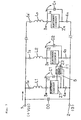
- Among causes which generate the failure of the electronic apparatus of this like, the cause of particular large weight is a conductive or a radioactive electromagnetic wave produced by a current (a sneak current) which flows through the parasitic capacity or the parasitic mutual inductance of a circuit, called a common mode phenomenon. Since the generation mechanism of the electromagnetic wave of this kind is complex, an effective countermeasure near the failure generation source which is considered most effective has not been established. Therefore, a conventional countermeasure has been to control the conduction or the radiation of the electromagnetic wave by electromagnetically shielding the whole electronic apparatus with a metallic cover and providing a common-mode choke coil or core for the cable outwardly extending from the apparatus. On the other hand, with reference to the printed-wiring board of the conventional type, as shown in Fig. 2, high frequency capacitors C1 - Cn are often connected between power supply terminals 3a - 3n and ground terminals 4a - 4n of electronic circuits Z1 - Zn such as the IC, LSI (hereinafter simply called an electronic circuit) connected respectively to power supply line 1 which corresponds to power source conductor layer 1 and grounding line 2 which corresponds to ground conductor layer 2 of the printed-wiring board. The purpose of this arrangement is to flow the high frequency current, which flows in power supply line 1 accompanying the high frequency operation of electronic circuits Z1 - Zn, in high frequency capacitors C1 - Cn to decrease (that is, filtering) the high frequency fluctuation of the power source terminal voltage and to restrict the coupling (that is, decoupling) with other electronic circuit sharing power supply line 1. However, in particular, for effectively reducing the fluctuation of the power supply voltage, the conventional printed-wiring board is structured, as shown in Fig. 1, with power source conductor layer 1 made of all flat plate having no wiring in order to lower the impedance of the power supply line. The conventional printing wiring board is structured, as shown in Fig 1, with insulative board layers 6, which are, e.g., typical resin substrates.
- The above conventional printed-wiring board has a problem that a circuit designer can not control the high frequency current which flows in the power supply line accompanying the high frequency operation of said electronic circuit.
- In other words, when the power conductor layer is made of a flat plate over the whole area without having wiring, the impedance of the power supply line is small, and hence even if a high frequency capacitor is connected between the power source terminal and the ground terminal of the electronic circuit, it is hard to control the high frequency power source current which flows out to the power supply line, and resultantly the high frequency power source current flows in the decoupling capacitor disposed in the vicinity of other electronic circuits which share the power supply line. Therefore, the analysis of the high frequency power source current with reference to the whole printed-wiring board is very difficult and hence it is unable to strictly select the decoupling capacitor to be used for each electronic circuit.
- Further, the distribution of the high frequency power source current on the whole printed-wiring board is very complex. Depending on the arrangement of electronic circuits on the printed-wiring board or on the operation state of the electronic circuits even if they are in the same arrangement, the high frequency power source current distributes in such a manner to form a large loop, having the probability of introducing the problem of electromagnetic radiation or immunity.
- For example, as shown in Fig. 2, electronic circuits Z1 (a large current), Z2 (a medium current) and Zn (a small current) for different high frequency power source currents are connected respectively to both power supply line 1 and ground line 2. Mainly from the mounting and the cost restrictions, capacitors C1, C2 and Cn of capacitance corresponding to respective high frequency power source currents (large capacitance for Z1, medium capacitance for Z2, small capacitance for Z3) are connected to respective electronic circuits. When the electronic circuits on the printed-wiring board operate in this state, since capacitor Cn of small capacitance, connected between the power source terminal and the ground terminal of electronic circuit Zn for small high frequency power source current, has the impedance larger than that of other capacitors, the high frequency power source current of electronic circuit Zn flows into capacitor C2 of medium capacitance (having small impedance compared to that of Zn) connected between the power source terminal and a ground terminal of electronic circuit Z2 for a medium high frequency power source current, or into capacitor C1 of large capacitance connected between the power source terminal and the ground terminal of electronic circuit Z1 for a large high frequency power source current. Further, if the capacitors are of the same type, the frequency characteristic of the impedance becomes different according to each capacitance, and the impedance of the capacitor of small capacitance tends to become smaller than the impedance of the capacitor having the larger capacitance, in the region where the number of the high frequency exceeds some value. Therefore, when viewed in the broad frequency band, electric currents flow to and fro in a complicated way between electronic circuits on the printed-wiring board. As a result, the loop made by the high frequency power source current becomes large or the high frequency current of the common mode is made to flow into such as the cable connected from one printed-wiring board to another printed-wiring board, thereby increasing the conductive or radioactive electromagnetic waves. These phenomena have caused the electromagnetic interference between the electronic apparatus, that is, EMC problem. Further, for example, high frequency power source voltage fluctuation with reference to one electronic circuit on the printed-wiring board sometimes becomes an issue. In this case, even if the capacitance of a decoupling capacitor in the vicinity of the electronic circuit is increased, it is not effective because the more the capacitance is increased, the more the high frequency power source currents of other electronic circuits flow into the circuit, and consequently it becomes hard to decrease the high frequency power source voltage fluctuation with the probability of failing in securing the high frequency operation of the electronic circuit.
- Further, when the latest IC/LSI is used in a logical unit which operates at a low frequency, for preventing the generation of the unnecessary conductive or radioactive electromagnetic waves to be caused due to excessively fast rise time or fall time of a rectangular wave signal of the IC/LSI, sometimes a high frequency filter is inserted in the circuit to slow the rise time and the fall time of the rectangular wave signal of the IC/LSI. However, when the high frequency filter of this like is newly added as parts, the high density mounting efficiency on the printed-wiring board is disadvantageously affected.
- EP 0 690 461 A1 describes a method to provide a device with a metallised magnetic substrate comprising a minimized inductor.
- Therefore, with the conventional printed-wiring board, it becomes necessary to electromagnetically shield the whole electronic apparatus with metal foil, as described above, to protect against the EMC problem and concurrently control the conduction of the electromagnetic waves by attaching a common-mode choke coil or core for the cable extending outwardly of the apparatus. Still further, with reference to the problem which hinders the high frequency operation of the IC/LSI, it is necessary to meet the problem by mounting capacitors of a required number or more on the printed-wiring board to control the high frequency power source voltage fluctuation of the whole wiring board.
- An object of the present invention is to provide a printed-wiring board which can remarkably reduce the generation of an electromagnetic noise, largely increase the-resistance to an extraneous electromagnetic noise, and allows the smooth high frequency operation of electronic circuits such as an IC, LSI to be mounted.
- Another object of the present invention is to provide a printed-wiring board for which a circuit designer can control the high frequency power source current of each electronic circuit such as an IC, LSI mounted on the wiring board.
- The printed-wiring board of the present invention is disclosed in claim 1.
- It is allowable to use a structure such that a capacitor is connected between a power supply side terminal and a ground side terminal of the electronic circuit, one end of the spiral coil inductor is connected to the power source terminal of the electronic circuit and the other end thereof is connected to the power source conductor layer. In this case, the spiral coil inductor constitutes a structural element of a decoupling circuit while discharging a large decoupling function with a small space.
- It is allowable to use a structure such that a high frequency filter is connected between an output terminal of one electronic circuit and an input terminal of an other electronic circuit, the high frequency filter including the spiral coil inductor as a structural element thereof. In this case, when the latest IC/LSI is used as the electronic circuit which operates at a low frequency, even if the rise time or the fall time of a rectangular wave signal of the IC/LSI is too fast, unnecessary conductive or radioactive electromagnetic waves are not generated.
- A part of the ground conductor layer and the power source conductor layer disposed opposite to each other may be used as two layers of conductor layers which constitute a spiral coil inductor. In this case, the spiral coil inductor is sometimes composed without using the additional number of conductor layers compared with the conventional case.
- Two layers of conductor layers used for composing the spiral coil inductor are each a part of the power source conductor layer and can have at least one layer of a ground layer outside of two conductor layers. In this case, unnecessary conductive or radioactive electromagnetic waves are not generated and the distortion of the signal waveform becomes minimum.
- Furthermore, it may take a structure having a viahole vertically connecting between two signal conductor layers while penetrating two conductor layers, and having another viahole connected to two ground conductor layers at both ends thereof being disposed in the proximity of the viahole. Also in this case, unnecessary electromagnetic waves are not generated and the signal waveform distortion becomes minimum.
- As an insulative magnetic material, a mixture of a ferrite fine powder of one of an Ni-Zn group, a Mn-Zn group, Sendust or a Li group and an insulative solvent may be used. Also as the insulative solvent, epoxy group insulative solvent can be used.
- Further, the insulative magnetic material can be formed of a plurality of magnetic films, with insulation coating on both sides of the insulative magnetic material. It is also possible to use a multilayer band of amorphous magnetic film as the plurality of magnetic film.
- The above and other objects, features and advantages of the present invention will become apparent from the following description with reference to the accompanying drawings which illustrate examples of the present invention.
-
- Fig. 1 is a longitudinal section of a conventional example of a printed-wiring board,
- Fig. 2 is a circuit diagram including electronic circuits of the printed-wiring board of Fig. 1,
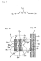
- Fig. 3 is a circuit symbol diagram of a spiral coil inductor which constitutes a primary part of an embodiment of the printed-wiring board of the present invention,
- Fig. 4A is a plan view of a first embodiment of the spiral coil inductor Ln of Fig. 3,
- Fig. 4B is a longitudinal section of Fig. 4A,
- Fig. 5 is a perspective view of the spiral coil inductor Ln of Fig. 4A,
- Fig. 6A is a plan view of a second embodiment of the spiral coil inductor Ln of Fig. 3,
- Fig. 6B is a longitudinal section of Fig. 6A,
- Fig. 7 is a circuit diagram showing an application example of the spiral coil inductor of Fig. 3,
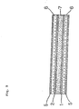
- Fig. 8 is a perspective view of the spiral coil inductor of Fig. 3,
- Fig. 9 is a longitudinal section of a four-layer printed-wiring board for constituting the spiral coil inductor of Fig. 3,
- Fig. 10 is a longitudinal section of a six-layer printed-wiring board for constituting the spiral coil inductor of Fig. 3,
- Fig. 11 is a longitudinal section of a six-layer printed-wiring board different from that of Fig. 10 and used for constituting the spiral coil inductor of Fig. 3,
- Fig. 12 is a longitudinal section of a six-layer printed-wiring board different from those of Fig. 10 and Fig. 11 and used for constituting the spiral coil inductor of Fig. 3,
- Fig. 13A is a graph showing measured results of the radiation field intensity in a radio wave darkroom with reference to the conventional example of the printed-wiring board,
- Fig. 13B is a graph showing measurement results similar to that of Fig. 13A prepared with reference to the embodiment of the printed-wiring board of the present invention,
- Fig. 14A is another graph showing the measurement result of Fig. 13A,
- Fig. 14B is another graph showing the measurement result of Fig. 13B,
- Fig. 15A is a measurement chart showing the magnetic field distribution in the vicinal area with reference to the conventional example of the printed-wiring board,
- Fig. 15B is a measurement chart showing the magnetic field distribution in the vicinal area with reference to the embodiment of the printed-wiring board of the present invention,
- Fig. 16 is a plan view showing the arrangement of I/O connectors of the embodiment of the printed-wiring board of the present invention,
- Fig. 17 is a diagram showing a measuring system for measuring a common-mode current which parallelly flows in an interface cable through the I/O connector.
- Fig. 18A is a graph showing the measurement result of the common-mode current of I/O connector (RS232C1) of the conventional example of the printed-wiring board,
- Fig. 18B is a graph showing the measurement result similar to that of Fig. 18A prepared with reference to the embodiment of the printed-wiring board of the present invention,
- Fig. 19A is a graph showing the measurement result of the common-mode current of I/O connector (RS232C2) of the conventional example of the printed-wiring board,
- Fig. 19B is a graph showing the measurement result similar to that of Fig. 19A prepared with reference to the embodiment of the printed-wiring board of the present invention,
- Fig. 20A is a graph showing the measurement result of the common-mode current of the I/O connector (keyboard/mouse) of the conventional example of the printed-wiring board,
- Fig. 20B is a graph showing the measurement result similar to that of Fig. 20A prepared with reference to the embodiment of the printed-wiring board of the present invention,
- Fig. 21A is a graph showing the measurement result of the common-mode current of the I/O connector (printer) of the conventional example of the printed-wiring board,
- Fig. 21B is a graph showing the measurement result similar to that of Fig. 21A prepared with reference to the embodiment of the printed-wiring board of the present invention.
-
- Fig. 3 shows circuit symbols of a spiral coil inductor which is a primary part of a printed-wiring board of the present invention, Fig. 4A and Fig. 4B show a plan view and a section of the spiral coil inductor Ln of a first embodiment of the printed-wiring board of Fig. 3, respectively. Terminal numbers 1n and 3n in the circuit symbols of Fig. 3 correspond to terminal numbers 1n and 3n of the plan view of Fig. 4A, respectively. In the first embodiment of the printed-wiring board, a part of two conductor layers 9, 10 disposed opposite to each other are cut out to produce a plurality of conductor layers 9a, 9b and 10a, lOb. In the whole region between two conductor layers 9a and 10a, 9b and 10b oppositely disposed to each other, there are provided insulative magnetic material 7 disposed in layers. By using viaholes 8a, 8b, 8c and 8d connecting between conductor layers 9a and 10a, 9b and 10b, and constructing as shown in perspective views of Fig. 4A, Fig. 4B and Fig. 5, spiral coil inductors each being an inductor of a spiral form are produced in the printed-wiring board.
- Figs. 6A and 6B show a plan view and a longitudinal section of the spiral coil inductor Ln of a second embodiment of the printed-wiring board of Fig. 3, respectively. In the printed-wiring board of the second embodiment, as shown in Figs. 6A and 6B, the structure is similar to that of the first embodiment except that insulative magnetic material 71 is disposed in layers to form the spiral coil inductor in a partial region between two layers of conductors 9a and 10a, 9b and 10b disposed facing each other.
- In the printed-wiring board of the first and the second embodiments, the spiral coil inductor is formed by using two layers of conductor layers. The inductance (L) of this coil is obtained in the following equation.
- µ0:
- permeability in the vacuum (4π10-7),
- µs:
- relative magnetic permeability,
- n:
- number of turns of spiral coil,
- s:
- cross-sectional area of spiral coil (m2),
- l:
- mean magnetic path length of spiral coil (m),
- For example, in case of composing a microstrip line in a well known meandering form, the microstrip line may take a structure (J.P.A. 236488/1995) in which the insulative magnetic material is disposed in layers on both sides of the conductor layer which constitutes the microstrip line, additionally providing ground conductor layers on both outsides of the magnetic material. However, in this case, the electrostatic coupling between the microstrip conductor layer and the neighboring ground conductor layer functions to control the impedance of the inductor. Therefore, even if the conductor length of the inductor is lengthened, when the wavelength of the current exceeds one half of the wavelength of the problematic high frequency current, characteristic impedance Z0 of the transmission line on the lossless line is given by equation (2). Specifically, Z0 becomes the constant impedance which is independent of the length of the conductor and the frequency of the applied current.
- C: capacitance (F) between conductors oppositely disposed, interposing a dielectric,
- L: inductance (H) of the microstrip line.
-
- Specifically, the insulative magnetic material generally shows relatively high permeability and also a relatively large dielectric constant. In the above equation (2), the value of C is proportional to the effective area and the dielectric constant of the conductors oppositely disposed, in other words, it is well known that C is proportional to the length of the conductor if the width of the conductor, the distance and the dielectric factor between the microstrip conductor layer and the ground conductor layer, are all constant. Similarly, with reference to the inductance when the microstrip is composed with one layer of the conductor in the same way as above in the meandering form, it is well known that the inductance is proportional to the length of the conductor if the width of the conductor and the effective permeability around the conductor are constant. Therefore, if the length of the conductor is prolonged, capacitance C and inductance L increase at the same rate, and hence characteristic impedance becomes always constant according to equation (2).
- On the other hand, with the spiral coil inductor according to the present invention, since the inductance L is proportional to the square of the number of turns of the coil, the value of L becomes proportional to the square of the length of the conductor, if the width of the conductor is constant. Therefore, according to the structure of the present invention, even if the inductor is placed between, for example, ground conductor layers to obtain the stable characteristic and reduce the interference on the signal conductor layer which is caused by the generated magnetic field, with reference to the value of the inductance L of the spiral coil inductor, the upper limit of the impedance of the inductor is not limited by said equation (2) and can take the larger value. Further, the more the frequency increases, the more it becomes possible to get the larger impedance.
- Although Figs. 4A, 4B and Figs. 6A, 6B show examples of the spiral coil inductor with the number of turns two, respectively, it is possible to get a large number of turns of the coil by increasing the number of conductors 9 and 10. In Fig. 4A, ℓ represents a mean magnetic path length, s in Fig. 4B an effective sectional area. Now, these values are structurally settled, and when the number of turns n is determined, the inductance L can be obtained through said equation (1).
- Fig. 7 shows a circuit in which the spiral coil inductor formed in such a way as described above is applied as a power source decoupling circuit of electronic circuits Z1 - Zn such as the IC, LSI which are mounted on the printed-wiring board and a part of a high frequency filter for prolonging the rise time or the fall time of the rectangular wave signal of the IC/LSI. In the printed-wiring board, one end of each of spiral coil inductors L1 - Ln designed to have an appropriate characteristic is connected to a power source terminal of each of electronic circuits Z1 - Zn, and each of the other ends is connected to power source conductor layer 1. Further, between power source terminals 3a - 3n and ground terminals 4a - 4n of electronic circuits, capacitors C1 - Cn of the proper characteristic are selectively connected, respectively. The high frequency power source currents produced by the high frequency operation of electronic circuits Z1 - Zn are effectively bypassed to respective capacitors, thereby controlling the high . frequency power source currents which leak out to power source terminal 1. This means that the value of capacitors C1 - Cn connected to electronic circuits Z1 - Zn, respectively, can be determined independently through the optimum design for every capacitor. Further, by concurrently setting the dimension of each conductor of spiral coil inductors L1 - Ln appropriately to get the resistance of a minute value, it becomes possible to control the fluctuation of the power source voltage of electronic circuits Z1 - Zn to a minute value.
- Now, high frequency filter F1 is connected between electronic circuits Z1 and Z2 of Fig. 7 by signal line 5. High frequency filter F1 is used for prolonging the rise time or the fall time of the rectangular wave signal of the IC/LSI, while having built-in spiral coil inductor L1 as a structural element. When the spiral coil inductor is used in the high frequency filter, even if the latest IC/LSI is applied in a logical unit which is operated at a low frequency, it becomes possible to effectively control, in mounting, the generation of the unnecessary conductive or radioactive electromagnetic wave which may be caused due to an excessively short rise time or fall time of the rectangular wave signal of the IC/LSI.
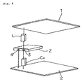
- Fig. 8 illustrates a connection structure shown with reference to one unit of the power source decoupling circuit selected from among circuit diagrams shown in Fig. 7. In this figure, it is important to make the high frequency power source current flow in the circuit easily by preparing the length of the path as short as possible particularly from power source terminal 3 of electronic circuit Z to ground terminal 4 of electronic circuit Z through capacitor Cn and ground layer 2.
- The printed-wiring board of Fig. 9 has four layers of conductor layers, the outer two layers serving as signal conductor layers 5, inner two layers serving as power source conductor layer 1 and ground conductor layer 2, respectively, and insulative magnetic substance 7 being disposed in layers between oppositely disposed power source conductor layer 1 and ground conductor layer 2.
- In the printed-wiring board, the spiral coil inductor Ln is formed by using power source conductor layer 1 and ground conductor layer 2. As insulative magnetic substance 7, a mixture of an Ni-Zn group ferrite fine powder and an insulation solvent of such as an epoxy group, or a mixture of a Mn-Zn group ferrite fine powder and an insulation solvent of such as an epoxy group, or a mixture of a Li group ferrite fine powder and an insulation solvent of such as an epoxy group is used.
- The printed-wiring board shown in Fig. 10 has six layers of conductor layers, the outermost two layers serving as signal conductor layers 5, the innermost two layers serving as power source conductor layer 1 while interposing insulative magnetic layer 7 and serving for forming the spiral coil inductor Ln. Two layers disposed outside both power conductor layers 1 serve as ground layers 2, respectively. If the spiral coil inductor according to the present invention is formed in a part of oppositely disposed two layers of power source conductor layers 1 which belong to six layer printed-wiring board of this like, the structure of the spiral coil inductor is as described before.
- The printed-wiring board shown in Fig. 11 comprises two layers of power source conductor layers 1 disposed opposite to each other for composing a spiral coil inductor, two layers of ground conductor layers 2 disposed outside both power source conductor layers 1, respectively, and viaholes 81 penetrating ground conductor layers 2 for vertically connecting between signal conductor layers, and further viaholes 82 disposed near said viaholes 81 being connected at both ends thereof to ground conductor layers 2. By constructing the printed-wiring board to this structure, with reference to viahole 81 for vertically connecting between the signal conductor layers, the unbalance of the impedance which may be produced near magnetic layer 7 can be controlled.
- In the printed-wiring board shown in Fig. 12, a multilayer band of the amorphous magnetic foil, is used as insulative magnetic material 7 disposed between two power source conductor layers. Insulation coating 11 is provided on both sides of the insulative magnetic material 7. As insulative magnetic material 7 to be disposed between conductor layers, it is of course possible to use other materials.
- The printed-wiring board according to the present embodiment has a built-in spiral coil inductor Ln composed by disposing insulative magnetic material in layers partially or wholly between two conductor layers facing each other, so that the large inductance can be obtained with a reduced space.
- A decoupling circuit composed by using said spiral coil inductor Ln can produce large decoupling effect with a reduced space.
- A high frequency filter composed by using said spiral coil inductor can prevent the generation of unnecessary conductive or radioactive electromagnetic waves which are caused by excessively shortened rise time or fall time of a rectangular wave signal of the IC/LSI, particularly when it is employed in the logical unit which operates at a low frequency.
- Now, the spiral coil inductor Ln, composed of a power source conductor layers and a ground conductor layer disposed opposite to each other and viaholes, has a number of layers not more than that of a conventional multilayer printed-wiring board, therefore it is advantageous to use from the viewpoint of cost when a small amount of the spiral coil inductor is required.
- Since a mixture of metal or a ferrite fine powder and an insulation solvent of such as an epoxy group is used as the magnetic material for composing the spiral coil inductor, the influence on the manufacturing process of the printed-wiring board can be kept to a lower level.
- When magnetic film is used as the magnetic material for composing the spiral coil inductor, the manufacturing process of the magnetic layer can be simplified.
- Next, a test result will be described with reference to a concrete example of the printed-wiring of the present embodiment.
- As shown in Figs. 3, 4 and 5, the printed wiring board (embodiment) to be tested is prepared by forming a spiral coil, using the wiring and a viahole, between a power source layer and an opposite layer both made of a flat plate, disposing a mixture of an Ni-Zn group ferrite fine powder and an insulation solvent of such as an epoxy group between both layers in layer form for the purpose of augmenting the inductance. Further, this printed-wiring board has a strengthened decoupling circuit as shown in Fig. 7. By placing an electronic apparatus (EWS: engineering work station) which uses this printed-wiring board in an electronic wave dark room, a tester measured the radiation field intensity (by VCCI measuring method). Thus measured results and the measured results of the conventional example are shown in Figs. 13A, 13B and Figs. 14A, 14B, respectively. Further, the results of Figs. 13A, 13B and Figs. 14A, 14B are shown in table 1.

- In the table, data in parentheses each represents a noise level. As shown in table 1, by comparing an original substrate (described as "conventional" in the table) having a conventional power source layer made of a flat plate as a whole and the embodiment of the present invention, it is known that the spectra of the multiplied waves (80 MHz, 320 MHz, 480 MHz, 600 MHz, 800 MHz, 860 MHz, 920 MHz) of the clock frequency (40 MHz) are more clearly controlled in the embodiment than in the original substrate, and the reduction effect of the radiation field can be recognized (spectra other than 80 MHz and 860 MHz are controlled to the background noise level).
- Further, in Figs. 15A, 15B, measurement results of the vicinity magnetic field distribution are shown, obtained by scanning a magnetic field measuring probe on the substrate of the conventional example and the embodiment (EWS), respectively. Although the measurement was performed for all the frequencies which showed the remarkable control effect in said radiation field intensity measurement, here the case of 80 MHz twice the clock frequency is shown as an example. In the distribution charts of Figs. 15A, 15B, a dark color portion represents the place where the magnetic field intensity is strong, and as the color becomes lighter, it represents that the magnetic field intensity decreases. In the dark color portion at the lower left part of the distribution chart, there exists a substrate mounted with a CPU and a large LSI which are noise generation sources. By comparing the distribution chart of Fig. 15A and Fig. 15B, it is understood that the magnetic field intensity of the periphery portion such as an upper part and a right side of Fig. 15B of the embodiment is weak (diffusion to the periphery is reduced). This means that the high frequency power source currents from the CPU and the large LSI which are the noise generation sources are effectively bypassed to the ground conductor by the decoupling capacitor disposed in the vicinity, thereby decreasing the wraparound of the currents to other electronic circuits. In other words, it shows that the decoupling effect has been increased due to the isolation realized by the individual LSI/IC unit.
- It is confirmed in the vicinity magnetic field distribution chart of Fig. 15B that the present embodiment has succeeded to increase the decoupling effect thereby decreasing the wraparound of the high frequency power source current to other circuit. Particularly, it is recognized that the diffusion to the upper right portion is decreased. It is to be noted that a similar tendency is confirmed with other frequencies. At the right side edge of the printed-wiring board which is an object of the present examination, there are provided as shown in Fig. 16, I/O connector (RS232C1) 11 for use as an interface to the outside, ditto (RS232C2) 12, ditto (printer) 13, and ditto (keyboard/mouse) 14. Accordingly, the fact that the diffusion of the high frequency current to the I/O connector portion has decreased, suggests that the current parallelly flows in the interface cable (called as a common-mode current) through the above I/O connectors 11 - 14 has also decreased. Therefore, in the measuring system shown in Fig. 17, the common-mode current parallelly flowing in the above interface cable 16 from the printed-wiring board 15 is measured by using a current probe 17. The results (current waveforms observed by a spectrum analyzer 18) are shown in Figs. 18A, 18B, Figs. 19A, 19B, Figs. 20A, 20B and Figs. 21A, 21B (only for 80 MHz). The measured data of the common-mode current are shown in table 2.
- The data in Fig. 18A - Fig. 21B are indicated by voltage between the both opposite ends of a terminal resister of probe 17 with unit of dB µ V.
- However, the relationship among the common currents can be recognized from the relationship among the measured data in Table 2.

- According to table 2, it is understood that the common-mode current decreases remarkably in the embodiment for all frequencies and connectors except RS232C1 connector with 360 MHz.
- As described above, by applying the present invention, the decoupling circuit is strengthened and the electromagnetic radiation noise from the electronic apparatus can largely be controlled.
- In the present embodiment, since the spiral coil inductor is structured with the inner layer of the printed-wiring board, no special parts are required to be mounted. Therefore, it can serve as the printed-wiring board of the high density mounting to effectively prevent the generation of the EMC problem.
- Further, since the design of the spiral coil inductor of the present invention can be performed together with the design of the wiring by means of a CAD tool for the printed-wiring board, a period for designing and manufacturing is remarkably reduced.
- Still further, according to the present invention, since the power source line for each electronic circuit such as the IC, LSI on the printed-wiring board is separated by the large high frequency impedance, the circuit designer can control the high frequency power source current on each of electronic circuits on the printed-wiring board. Therefore, when a designing problem is produced related with the high frequency operation of electronic circuits of this like, it can be settled sooner than ever.
- Further, the high frequency operation of electronic circuits such as the IC, LSI on the printed-wiring board will become stabilized. Consequently, it can contribute to the promotion of high speed clock multimedia equipment. The reason for this is that when a spiral coil inductor which gives high impedance with the high frequency wave and a capacitor which gives low impedance with the high frequency wave are used, if the power source line is viewed from the electronic circuits such as the IC, LSI, the impedance becomes very low thereby making it possible to control the distortion of the signal waveform which may be caused by source voltage fluctuation, while if said electronic circuits are viewed from the common power source line, the impedance becomes very high thereby becoming able to control the wraparound of the high frequency power source current from electronic circuits such as other IC, LSI connected to the common power source line.
- Further, the printed-wiring board according to the present invention is excellent in economical efficiency and reliability quality. The reason is that the spiral coil inductor is composed of the inner layer of the printed-wiring board and hence the spiral coil inductor is also manufactured according to a high technique at the same time when the printed-wiring board is manufactured.
Claims (20)
- A printed-wiring board comprising at least one electronic circuit; and a substrate for mounting said electronic circuit, wherein said substrate comprises:characterized in that a first end of said coil inductor is connected to a power source terminal of said electronic circuit and a second end of said coil inductor is connected to a first power source conductor layer.two or more conductor layers (9, 10);a coil inductor composed of a plurality of conductor strips (9a, 9b, 10a, 10b) formed by cutting a part of a pair of conductor layers (9, 10) disposed opposite to each other from among said conductor layers (9, 10), and viaholes (8a, 8b, 8c, 8d) vertically connecting said plurality of conductor strips (9a, 9b, 10a, 10b);an insulative magnetic material (7) being disposed between said pair of conductor layers facing each other used for composing said coil inductor; and
- A printed-wiring board according to claim 1, wherein said insulative magnetic material (7) is disposed in the whole region between said pair of conductor layers (9, 10) disposed opposite to each other.
- A printed-wiring board according to claim 1, wherein said insulative magnetic material is disposed only in a part of the region between said pair of conductor layers where said plurality of conductor strips are formed.
- A printed-wiring board according to claim 1, further comprising a capacitor connected between said power source terminal and a ground terminal of said electronic circuit.
- A printed-wiring board according to claim 1, further comprising a high frequency filter connected between an output terminal of one electronic circuit and an input terminal of an other electronic circuit, wherein said coil inductor is used as a composition element of said high frequency filter.
- A printed-wiring board according to claim 1, wherein said electronic circuit is an IC.
- A printed-wiring board according to claim 1, wherein said electronic circuit is an LSI.
- A printed-wiring board according to claim 1, wherein said pair of conductor layers (9, 10) which are used for composing said coil inductor are apart of a ground conductor layer and a part of said first power source conductor layer oppositely disposed to each other.
- A printed-wiring board according to claim 1, further comprising:a second power source conductor layer; wherein said first and second power source conductor layers are used as said pair of conductor layers (9, 10) which composing said coil inductor; and at least one ground layer outside said pair of conductor layers (9, 10) respectively.
- A printed-wiring board according to claim 1 further comprising: a first viahole penetrating said pair of conductor layers (9, 10) used for composing said coil inductor while connecting two signal conductor layers; and a second viahole connecting two ground conductor layers, being disposed in the proximity of said viahole.
- A printed-wiring board according to claim 1, wherein a mixture of an Ni-Zn group ferrite fine powder and an insulation solvent is used as said insulative magnetic material.
- A printed-wiring board according to claim 1, wherein a mixture of a Mn-Zn group ferrite fine powder and an insulation solvent is used as said insulative magnetic material.
- A printed-wiring board according to claim 1, wherein a mixture of a SENDUST fine powder and an insulation solvent is used as said insulative magnetic material.
- A printed-wiring board according to claim 1, wherein a mixture of a Li group ferrite fine powder and an insultion solvent is used as said insulative magnetic material.
- A printed-wiring board according to claim 11, wherein said insulation solvent is an epoxy group insulation solvent.
- A printed-wiring board according to claim 12, wherein said insulation solvent is an epoxy group insulation solvent.
- A printed-wiring board according to claim 13, wherein said insulation solvent is an epoxy group insulation solvent.
- A printed-wiring board according to claim 14, wherein said insulation solvent is the epoxy group insulation solvent.
- A printed-wiring board according to claim 1, wherein said insulation magnetic material comprises:a magnetic material layer formed of a plurality of magnetic films;a first insulation coating applied to an upper surface of said magnetic material layer; anda second insulation coating applied to a lower surface of said magnetic material layer.
- A printed-wiring board according to claim 19, wherein said plurality of magnetic films comprise amorphous magnetic films.
Applications Claiming Priority (6)
| Application Number | Priority Date | Filing Date | Title |
|---|---|---|---|
| JP13220297 | 1997-05-22 | ||
| JP132202/97 | 1997-05-22 | ||
| JP13220297 | 1997-05-22 | ||
| JP9253519A JPH1140915A (en) | 1997-05-22 | 1997-09-18 | Printed wiring board |
| JP25351997 | 1997-09-18 | ||
| JP253519/97 | 1997-09-18 |
Publications (3)
| Publication Number | Publication Date |
|---|---|
| EP0880150A2 EP0880150A2 (en) | 1998-11-25 |
| EP0880150A3 EP0880150A3 (en) | 1999-08-18 |
| EP0880150B1 true EP0880150B1 (en) | 2003-03-19 |
Family
ID=26466836
Family Applications (1)
| Application Number | Title | Priority Date | Filing Date |
|---|---|---|---|
| EP98109129A Expired - Lifetime EP0880150B1 (en) | 1997-05-22 | 1998-05-19 | Printed wiring board |
Country Status (9)
| Country | Link |
|---|---|
| US (1) | US5978231A (en) |
| EP (1) | EP0880150B1 (en) |
| JP (1) | JPH1140915A (en) |
| KR (1) | KR100294957B1 (en) |
| CN (1) | CN1083684C (en) |
| AU (1) | AU704127B2 (en) |
| CA (1) | CA2237677C (en) |
| DE (1) | DE69812221T2 (en) |
| TW (1) | TW374975B (en) |
Families Citing this family (65)
| Publication number | Priority date | Publication date | Assignee | Title |
|---|---|---|---|---|
| US7336468B2 (en) | 1997-04-08 | 2008-02-26 | X2Y Attenuators, Llc | Arrangement for energy conditioning |
| US7301748B2 (en) | 1997-04-08 | 2007-11-27 | Anthony Anthony A | Universal energy conditioning interposer with circuit architecture |
| US7321485B2 (en) | 1997-04-08 | 2008-01-22 | X2Y Attenuators, Llc | Arrangement for energy conditioning |
| US9054094B2 (en) | 1997-04-08 | 2015-06-09 | X2Y Attenuators, Llc | Energy conditioning circuit arrangement for integrated circuit |
| US6103134A (en) * | 1998-12-31 | 2000-08-15 | Motorola, Inc. | Circuit board features with reduced parasitic capacitance and method therefor |
| US6570994B1 (en) * | 1999-03-25 | 2003-05-27 | Agere Systems Inc. | Field layer speaker for consumer products |
| JP3255151B2 (en) * | 1999-05-11 | 2002-02-12 | 日本電気株式会社 | Multilayer printed circuit board |
| JP3267274B2 (en) * | 1999-08-13 | 2002-03-18 | 日本電気株式会社 | Multilayer printed circuit board |
| CN1240086C (en) | 2000-05-19 | 2006-02-01 | P·A·哈丁 | Slot core transformers |
| US20020121943A1 (en) * | 2000-05-25 | 2002-09-05 | Alexander Axelrod | EMI filters based on amorphous metals in a form of a microwire, a ribbon and/or a powder |
| AU2001294646A1 (en) * | 2000-09-22 | 2002-04-02 | M-Flex Multi-Fineline Electronix, Inc. | Electronic transformer/inductor devices and methods for making same |
| CN1230840C (en) * | 2000-11-21 | 2005-12-07 | 皇家菲利浦电子有限公司 | System, printed circuit board, charger device, user device, and apparatus |
| JP2002259478A (en) | 2001-02-28 | 2002-09-13 | Nec Corp | Integrated digital circuit design system and design method |
| JP2002335107A (en) | 2001-05-08 | 2002-11-22 | Nec Corp | Transmission line type component |
| US7016490B2 (en) | 2001-05-21 | 2006-03-21 | Conexant Systems, Inc. | Circuit board capacitor structure for forming a high voltage isolation barrier |
| TWI279080B (en) * | 2001-09-20 | 2007-04-11 | Nec Corp | Shielded strip line device and method of manufacture thereof |
| DE10154833A1 (en) * | 2001-11-08 | 2003-05-22 | Infineon Technologies Ag | Inductor and process for its manufacture |
| US6489853B1 (en) | 2002-03-19 | 2002-12-03 | Z-Communications, Inc. | Low phase noise oscillator |
| JP2004104420A (en) * | 2002-09-09 | 2004-04-02 | Fujitsu Ten Ltd | Signal transmission circuit and electronic equipment |
| US7135952B2 (en) | 2002-09-16 | 2006-11-14 | Multi-Fineline Electronix, Inc. | Electronic transformer/inductor devices and methods for making same |
| US6972967B2 (en) * | 2003-02-20 | 2005-12-06 | Avaya Technology Group | EMC/ESD mitigation module |
| WO2004082065A1 (en) * | 2003-03-12 | 2004-09-23 | Nec Corporation | Power supply distribution circuit |
| US20040197284A1 (en) * | 2003-04-04 | 2004-10-07 | Frederic Auguste | Cosmetic composition comprising a volatile fatty phase |
| JP4506303B2 (en) * | 2003-08-29 | 2010-07-21 | 株式会社デンソー | Electronic control unit |
| DE10343362B4 (en) * | 2003-09-15 | 2005-09-22 | Institut für Maschinen, Antriebe und elektronische Gerätetechnik gGmbH - IMG | Method for producing a printed circuit board with improved EMC behavior |
| US7237217B2 (en) * | 2003-11-24 | 2007-06-26 | International Business Machines Corporation | Resonant tree driven clock distribution grid |
| CN1890854A (en) | 2003-12-22 | 2007-01-03 | X2Y艾泰钮埃特有限责任公司 | Internally shielded energy conditioner |
| US7310243B2 (en) * | 2004-06-10 | 2007-12-18 | International Business Machines Corporation | Method and components for implementing EMC shielded resonance damping |
| KR100603632B1 (en) * | 2004-10-29 | 2006-07-24 | 수퍼나노텍(주) | A sensing board excelent in high frequency feature, and method for manufacturing the same |
| US7436282B2 (en) | 2004-12-07 | 2008-10-14 | Multi-Fineline Electronix, Inc. | Miniature circuitry and inductive components and methods for manufacturing same |
| AU2005314077B2 (en) | 2004-12-07 | 2010-08-05 | Multi-Fineline Electronix, Inc. | Miniature circuitry and inductive components and methods for manufacturing same |
| GB2439861A (en) | 2005-03-01 | 2008-01-09 | X2Y Attenuators Llc | Internally overlapped conditioners |
| US7817397B2 (en) | 2005-03-01 | 2010-10-19 | X2Y Attenuators, Llc | Energy conditioner with tied through electrodes |
| US7221251B2 (en) * | 2005-03-22 | 2007-05-22 | Acutechnology Semiconductor | Air core inductive element on printed circuit board for use in switching power conversion circuitries |
| EP1991996A1 (en) | 2006-03-07 | 2008-11-19 | X2Y Attenuators, L.L.C. | Energy conditioner structures |
| US7645941B2 (en) | 2006-05-02 | 2010-01-12 | Multi-Fineline Electronix, Inc. | Shielded flexible circuits and methods for manufacturing same |
| US7636242B2 (en) * | 2006-06-29 | 2009-12-22 | Intel Corporation | Integrated inductor |
| JP4859700B2 (en) * | 2007-02-20 | 2012-01-25 | セイコーエプソン株式会社 | Coil unit and electronic equipment |
| KR100838244B1 (en) | 2007-06-22 | 2008-06-17 | 삼성전기주식회사 | Electromagnetic bandgap structure and printed circuit board |
| US8169790B2 (en) * | 2007-08-07 | 2012-05-01 | Samsung Electro-Mechanics Co., Ltd. | Electromagnetic bandgap structure and printed circuit board |
| US8310840B2 (en) * | 2007-08-07 | 2012-11-13 | Samsung Electro-Mechanics Co., Ltd. | Electromagnetic bandgap structure and printed circuit board |
| TWI345243B (en) * | 2007-08-14 | 2011-07-11 | Ind Tech Res Inst | Inter-helix inductor devices |
| KR101038234B1 (en) * | 2009-02-24 | 2011-06-01 | 삼성전기주식회사 | Electromagnetic interference noise reduction board using electromagnetic bandgap structure |
| KR101055483B1 (en) * | 2009-04-07 | 2011-08-08 | 포항공과대학교 산학협력단 | Electromagnetic bandgap structure and printed circuit board including the same |
| JP2011101327A (en) * | 2009-11-09 | 2011-05-19 | Canon Inc | Signal transmission line |
| CN102065636A (en) * | 2009-11-12 | 2011-05-18 | 群康科技(深圳)有限公司 | Circuit board as well as electronic device and liquid crystal display applying same |
| JP5724804B2 (en) * | 2011-09-30 | 2015-05-27 | 株式会社村田製作所 | Circuit module |
| JP6086370B2 (en) * | 2012-03-16 | 2017-03-01 | 学校法人福岡大学 | Inductor built-in substrate manufacturing method, inductor built-in substrate, and power supply module using the same |
| WO2014115678A1 (en) * | 2013-01-22 | 2014-07-31 | 株式会社村田製作所 | High frequency signal transmission line, and electronic apparatus |
| WO2014119410A1 (en) * | 2013-01-29 | 2014-08-07 | 株式会社村田製作所 | High-frequency-signal transmission line, and electronic device |
| CN204464431U (en) * | 2013-01-29 | 2015-07-08 | 株式会社村田制作所 | High frequency signal transmission line and electronic equipment |
| JP6353642B2 (en) * | 2013-02-04 | 2018-07-04 | 株式会社トーキン | Magnetic core, inductor, and module with inductor |
| JP6012539B2 (en) * | 2013-05-08 | 2016-10-25 | 本田技研工業株式会社 | Noise filter |
| WO2016111282A1 (en) * | 2015-01-07 | 2016-07-14 | 株式会社村田製作所 | Coil component |
| CN110351949B (en) * | 2016-02-02 | 2022-04-15 | 景硕科技股份有限公司 | Layer-adding carrier plate structure with magnetic induction coil and soft plate |
| US10256028B2 (en) | 2016-03-31 | 2019-04-09 | Kinsus Interconnect Technology Corp. | Buildup board structure |
| EP3346478B1 (en) * | 2017-01-09 | 2019-05-01 | Siemens Aktiengesellschaft | Capacitor system and subsea electrical system comprising it |
| JP6852415B2 (en) * | 2017-01-24 | 2021-03-31 | 大日本印刷株式会社 | Manufacturing method of mounting substrate and through electrode substrate including through electrode substrate and through electrode substrate |
| KR102562793B1 (en) | 2017-12-06 | 2023-08-03 | 삼성전자주식회사 | Prinred circuit and electronic device including the same |
| CN108599396B (en) * | 2018-06-14 | 2023-11-03 | 西安电掣风云智能科技有限公司 | Ultra-thin wide-frequency medium-and-long-distance wireless power transmission coil |
| US11500433B2 (en) | 2020-01-14 | 2022-11-15 | Au Optronics Corporation | Flexible electronic device |
| TW202032226A (en) * | 2020-01-14 | 2020-09-01 | 友達光電股份有限公司 | Structure of flexible circuits |
| CN111475064B (en) * | 2020-04-17 | 2022-05-24 | 深圳市鸿合创新信息技术有限责任公司 | Transparent coil plate and manufacturing method thereof, transparent electromagnetic induction plate and display device |
| CN111462687B (en) * | 2020-06-09 | 2021-05-25 | 上海天马有机发光显示技术有限公司 | Display panel, driving method thereof and display device |
| CN112004310B (en) * | 2020-08-24 | 2023-09-01 | 大连吉星电子股份有限公司 | Flexible circuit board for enabling 5G signals to be stably transmitted |
Family Cites Families (11)
| Publication number | Priority date | Publication date | Assignee | Title |
|---|---|---|---|---|
| LU83316A1 (en) * | 1981-04-24 | 1981-07-24 | Siemens Ag | HYBRID COIL AND METHOD FOR THE PRODUCTION THEREOF |
| JPS60196910A (en) * | 1984-03-19 | 1985-10-05 | Fujitsu Ltd | Hybrid integrated circuit and manufacture thereof |
| JPS62139395A (en) * | 1985-12-13 | 1987-06-23 | 松下電器産業株式会社 | Multi-function circuit board |
| JPH02280410A (en) * | 1989-04-20 | 1990-11-16 | Takeshi Ikeda | Lc noise filter |
| US5055816A (en) * | 1989-06-26 | 1991-10-08 | Motorola, Inc. | Method for fabricating an electronic device |
| US4984146A (en) * | 1990-03-27 | 1991-01-08 | International Business Machines Corporation | Suppression of radiated EMI for power supplies |
| JP2829151B2 (en) * | 1991-03-04 | 1998-11-25 | メルコアジャパン株式会社 | Conductive material bonding element and circuit configuration |
| US5349743A (en) * | 1991-05-02 | 1994-09-27 | At&T Bell Laboratories | Method of making a multilayer monolithic magnet component |
| DE4306416A1 (en) * | 1993-03-02 | 1994-09-08 | Kolbe & Co Hans | Coil structure for a printed circuit board arrangement |
| TW265450B (en) * | 1994-06-30 | 1995-12-11 | At & T Corp | Devices using metallized magnetic substrates |
| JP2734447B2 (en) * | 1995-09-14 | 1998-03-30 | 日本電気株式会社 | Multilayer printed circuit board |
-
1997
- 1997-09-18 JP JP9253519A patent/JPH1140915A/en active Pending
-
1998
- 1998-05-06 TW TW087107029A patent/TW374975B/en not_active IP Right Cessation
- 1998-05-14 CA CA002237677A patent/CA2237677C/en not_active Expired - Fee Related
- 1998-05-19 EP EP98109129A patent/EP0880150B1/en not_active Expired - Lifetime
- 1998-05-19 DE DE69812221T patent/DE69812221T2/en not_active Expired - Fee Related
- 1998-05-21 AU AU68029/98A patent/AU704127B2/en not_active Ceased
- 1998-05-21 US US09/082,800 patent/US5978231A/en not_active Expired - Fee Related
- 1998-05-21 CN CN98101485A patent/CN1083684C/en not_active Expired - Fee Related
- 1998-05-21 KR KR1019980018295A patent/KR100294957B1/en not_active IP Right Cessation
Also Published As
| Publication number | Publication date |
|---|---|
| US5978231A (en) | 1999-11-02 |
| DE69812221T2 (en) | 2004-02-05 |
| CN1201366A (en) | 1998-12-09 |
| KR100294957B1 (en) | 2001-07-12 |
| CN1083684C (en) | 2002-04-24 |
| KR19980087247A (en) | 1998-12-05 |
| TW374975B (en) | 1999-11-21 |
| CA2237677C (en) | 2002-03-26 |
| EP0880150A3 (en) | 1999-08-18 |
| JPH1140915A (en) | 1999-02-12 |
| AU704127B2 (en) | 1999-04-15 |
| EP0880150A2 (en) | 1998-11-25 |
| DE69812221D1 (en) | 2003-04-24 |
| AU6802998A (en) | 1998-11-26 |
| CA2237677A1 (en) | 1998-11-22 |
Similar Documents
| Publication | Publication Date | Title |
|---|---|---|
| EP0880150B1 (en) | Printed wiring board | |
| KR100294956B1 (en) | Reducing electromagnetic noise radiated from a printed board | |
| KR100382804B1 (en) | Multilayer print substrate | |
| JP3055488B2 (en) | Multilayer printed circuit board and method of manufacturing the same | |
| US5357050A (en) | Apparatus and method to reduce electromagnetic emissions in a multi-layer circuit board | |
| EP0470031B1 (en) | Circuit board EMI suppressor | |
| US6215372B1 (en) | Method and apparatus for reducing electrical resonances in power and noise propagation in power distribution circuits employing plane conductors | |
| JP3255151B2 (en) | Multilayer printed circuit board | |
| EP0982813B1 (en) | Method for reducing RF electromagnetic emissions | |
| EP0631460B1 (en) | Printed circuit board | |
| JP2734447B2 (en) | Multilayer printed circuit board | |
| EP1232679B1 (en) | Printed circuit board employing lossy power distribution network to reduce power plane resonances | |
| US6150895A (en) | Circuit board voltage plane impedance matching | |
| JP3214472B2 (en) | Multilayer printed circuit board | |
| US20030062965A1 (en) | Circuit board having ferrite containing layer | |
| US6297965B1 (en) | Wiring arrangement including capacitors for suppressing electromagnetic wave radiation from a printed circuit board | |
| US6706974B2 (en) | Plane splits filled with lossy materials | |
| US5912597A (en) | Printed circuit board | |
| EP0719078B1 (en) | Printed circuit assembly having improved reference plane isolation | |
| US6215076B1 (en) | Printed circuit board with noise suppression | |
| JP2991136B2 (en) | Multilayer printed circuit board and method of manufacturing the same | |
| JP2001326468A (en) | Multilayer printed wiring board and electronic apparatus | |
| JPH0621154A (en) | Tape carrier for tab |
Legal Events
| Date | Code | Title | Description |
|---|---|---|---|
| PUAI | Public reference made under article 153(3) epc to a published international application that has entered the european phase |
Free format text: ORIGINAL CODE: 0009012 |
|
| AK | Designated contracting states |
Kind code of ref document: A2 Designated state(s): DE FR GB |
|
| AX | Request for extension of the european patent |
Free format text: AL;LT;LV;MK;RO;SI |
|
| PUAL | Search report despatched |
Free format text: ORIGINAL CODE: 0009013 |
|
| AK | Designated contracting states |
Kind code of ref document: A3 Designated state(s): AT BE CH CY DE DK ES FI FR GB GR IE IT LI LU MC NL PT SE |
|
| AX | Request for extension of the european patent |
Free format text: AL;LT;LV;MK;RO;SI |
|
| RIC1 | Information provided on ipc code assigned before grant |
Free format text: 6H 01F 17/00 A, 6H 05K 1/16 B |
|
| 17P | Request for examination filed |
Effective date: 19990707 |
|
| AKX | Designation fees paid |
Free format text: DE FR GB |
|
| 17Q | First examination report despatched |
Effective date: 20010903 |
|
| GRAH | Despatch of communication of intention to grant a patent |
Free format text: ORIGINAL CODE: EPIDOS IGRA |
|
| GRAH | Despatch of communication of intention to grant a patent |
Free format text: ORIGINAL CODE: EPIDOS IGRA |
|
| GRAA | (expected) grant |
Free format text: ORIGINAL CODE: 0009210 |
|
| AK | Designated contracting states |
Designated state(s): DE FR GB |
|
| REG | Reference to a national code |
Ref country code: GB Ref legal event code: FG4D |
|
| REF | Corresponds to: |
Ref document number: 69812221 Country of ref document: DE Date of ref document: 20030424 Kind code of ref document: P |
|
| ET | Fr: translation filed | ||
| PLBE | No opposition filed within time limit |
Free format text: ORIGINAL CODE: 0009261 |
|
| STAA | Information on the status of an ep patent application or granted ep patent |
Free format text: STATUS: NO OPPOSITION FILED WITHIN TIME LIMIT |
|
| 26N | No opposition filed |
Effective date: 20031222 |
|
| PGFP | Annual fee paid to national office [announced via postgrant information from national office to epo] |
Ref country code: FR Payment date: 20090515 Year of fee payment: 12 Ref country code: DE Payment date: 20090514 Year of fee payment: 12 |
|
| PGFP | Annual fee paid to national office [announced via postgrant information from national office to epo] |
Ref country code: GB Payment date: 20090513 Year of fee payment: 12 |
|
| GBPC | Gb: european patent ceased through non-payment of renewal fee |
Effective date: 20100519 |
|
| REG | Reference to a national code |
Ref country code: FR Ref legal event code: ST Effective date: 20110131 |
|
| PG25 | Lapsed in a contracting state [announced via postgrant information from national office to epo] |
Ref country code: DE Free format text: LAPSE BECAUSE OF NON-PAYMENT OF DUE FEES Effective date: 20101201 |
|
| PG25 | Lapsed in a contracting state [announced via postgrant information from national office to epo] |
Ref country code: FR Free format text: LAPSE BECAUSE OF NON-PAYMENT OF DUE FEES Effective date: 20100531 |
|
| PG25 | Lapsed in a contracting state [announced via postgrant information from national office to epo] |
Ref country code: GB Free format text: LAPSE BECAUSE OF NON-PAYMENT OF DUE FEES Effective date: 20100519 |