EP0875771A2 - Senseur opto-électronique avec des éléments photosensibles arangés en ligne ou matrice - Google Patents
Senseur opto-électronique avec des éléments photosensibles arangés en ligne ou matrice Download PDFInfo
- Publication number
- EP0875771A2 EP0875771A2 EP98107139A EP98107139A EP0875771A2 EP 0875771 A2 EP0875771 A2 EP 0875771A2 EP 98107139 A EP98107139 A EP 98107139A EP 98107139 A EP98107139 A EP 98107139A EP 0875771 A2 EP0875771 A2 EP 0875771A2
- Authority
- EP
- European Patent Office
- Prior art keywords
- light
- sensor arrangement
- useful
- photosensitive elements
- transmission
- Prior art date
- Legal status (The legal status is an assumption and is not a legal conclusion. Google has not performed a legal analysis and makes no representation as to the accuracy of the status listed.)
- Granted
Links
Images


Classifications
-
- G—PHYSICS
- G01—MEASURING; TESTING
- G01S—RADIO DIRECTION-FINDING; RADIO NAVIGATION; DETERMINING DISTANCE OR VELOCITY BY USE OF RADIO WAVES; LOCATING OR PRESENCE-DETECTING BY USE OF THE REFLECTION OR RERADIATION OF RADIO WAVES; ANALOGOUS ARRANGEMENTS USING OTHER WAVES
- G01S17/00—Systems using the reflection or reradiation of electromagnetic waves other than radio waves, e.g. lidar systems
- G01S17/02—Systems using the reflection of electromagnetic waves other than radio waves
- G01S17/06—Systems determining position data of a target
- G01S17/46—Indirect determination of position data
-
- G—PHYSICS
- G01—MEASURING; TESTING
- G01S—RADIO DIRECTION-FINDING; RADIO NAVIGATION; DETERMINING DISTANCE OR VELOCITY BY USE OF RADIO WAVES; LOCATING OR PRESENCE-DETECTING BY USE OF THE REFLECTION OR RERADIATION OF RADIO WAVES; ANALOGOUS ARRANGEMENTS USING OTHER WAVES
- G01S7/00—Details of systems according to groups G01S13/00, G01S15/00, G01S17/00
- G01S7/48—Details of systems according to groups G01S13/00, G01S15/00, G01S17/00 of systems according to group G01S17/00
- G01S7/483—Details of pulse systems
- G01S7/486—Receivers
- G01S7/4861—Circuits for detection, sampling, integration or read-out
- G01S7/4863—Detector arrays, e.g. charge-transfer gates
-
- G—PHYSICS
- G01—MEASURING; TESTING
- G01S—RADIO DIRECTION-FINDING; RADIO NAVIGATION; DETERMINING DISTANCE OR VELOCITY BY USE OF RADIO WAVES; LOCATING OR PRESENCE-DETECTING BY USE OF THE REFLECTION OR RERADIATION OF RADIO WAVES; ANALOGOUS ARRANGEMENTS USING OTHER WAVES
- G01S7/00—Details of systems according to groups G01S13/00, G01S15/00, G01S17/00
- G01S7/48—Details of systems according to groups G01S13/00, G01S15/00, G01S17/00 of systems according to group G01S17/00
- G01S7/483—Details of pulse systems
- G01S7/486—Receivers
- G01S7/487—Extracting wanted echo signals, e.g. pulse detection
- G01S7/4873—Extracting wanted echo signals, e.g. pulse detection by deriving and controlling a threshold value
-
- G—PHYSICS
- G01—MEASURING; TESTING
- G01S—RADIO DIRECTION-FINDING; RADIO NAVIGATION; DETERMINING DISTANCE OR VELOCITY BY USE OF RADIO WAVES; LOCATING OR PRESENCE-DETECTING BY USE OF THE REFLECTION OR RERADIATION OF RADIO WAVES; ANALOGOUS ARRANGEMENTS USING OTHER WAVES
- G01S7/00—Details of systems according to groups G01S13/00, G01S15/00, G01S17/00
- G01S7/48—Details of systems according to groups G01S13/00, G01S15/00, G01S17/00 of systems according to group G01S17/00
- G01S7/483—Details of pulse systems
- G01S7/486—Receivers
- G01S7/487—Extracting wanted echo signals, e.g. pulse detection
- G01S7/4876—Extracting wanted echo signals, e.g. pulse detection by removing unwanted signals
Definitions
- the invention relates to an opto-electronic sensor arrangement with a light transmitter for sending successive Useful light pulses in a monitoring area and one Light receiver unit for receiving one in the surveillance area reflected object reflected useful light pulses.
- the light receiver units can for example several photosensitive elements include, so that after a suitable evaluation of the Photosensitive elements delivered signals to the position of the reflecting object in the surveillance area can be closed.
- PSDs position sensitive detectors
- CCDs position sensitive detectors
- An object of the invention is an opto-electronic Sensor arrangement of the type mentioned to further develop such that an improved extraneous light, in particular Constant light suppression is made possible.
- this object is achieved in that an opto-electronic sensor arrangement of the type mentioned, in which the light receiver unit has at least two photosensitive Elements, each photosensitive element each assigned a circuit for extraneous light suppression becomes.
- Each photosensitive element is thus in accordance with the invention with its own separate extraneous light suppression circuit equipped.
- the principle according to the invention enables particularly reliable and effective suppression of extraneous light, which, for example, also enables reliable detection of useful light signals when the dynamic range of the useful light signal is significantly smaller than the dynamic range of the extraneous light.
- the opto-electronic according to the invention Sensor arrangement advantageous that due to the in each Cell of a row or an array or with respect to each photosensitive Elements separate suppression of extraneous light differently illuminated background areas no negative effects on the useful light signal evaluation to have.
- the received useful light gives according to the invention always correct information about the reflectivity of objects or background elements in the surveillance area, independently of how these objects or background elements be illuminated by extraneous light.
- the suppression of extraneous light in an opto-electronic according to the invention can also be improved by that only relatively short useful light pulses, in particular those with high energy.
- the duration of the Useful light pulses can be in the ns range, for example.
- the pulse duration of the useful light signal can preferably be between 1 ⁇ s and 20 ⁇ s. It is advantageous if the reciprocal the pulse duration of the useful light by approximately two orders of magnitude lies above the highest occurring stray light frequency, because then a particularly reliable interference or external light suppression becomes possible.
- a device according to the invention is particularly advantageous Sensor arrangement when a variety of photosensitive Elements side by side in a row or matrix arrangement be provided. Especially with a matrix arrangement it is possible according to the invention, not only that Presence of an object in the surveillance room but also to determine its position.
- each of the circuits for suppression of extraneous light one with the respective Regulated photosensitive element Energy source, especially a power source.
- This energy source provides the through the photosensitive element flowing current, which in the breaks between the Useful light pulse emissions correspond to the existing ambient light.
- the electricity supplied by the named energy source is then according to the invention also during the transmission of useful light signals kept at the value determined last or in the time range of a useful light signal transmission extrapolated extraneous light curve corresponds.
- the additional when receiving useful light through the photosensitive Element flowing current becomes another Energy source, in particular related to a capacitor, wherein the measurable value of this additional current ultimately corresponds to the received useful light.
- the regulation changeable in times of the transmission of the useful light pulses compared to the regulation in the pauses between the transmission of the useful light pulses, the change in the regulating behavior being able to be effected in particular by activating and deactivating at least one filter of a regulating circuit.
- a filter with a shorter time constant can be activated in the pauses between the transmission of the useful light pulses than during the transmission of the useful light pulses. The latter procedure allows extrapolation of the current supplied by the energy source as a function of its course in the pauses between the transmission of useful light during the transmission of the useful light pulses, so that the external light compensation is additionally improved.
- Each of the circuits for extraneous light suppression can be equipped with a Storage element for storing the photosensitive Element received useful light portion are provided, the storage element being designed in particular as a capacitor becomes.
- the memory element can be received during the useful light pulse reception can be coupled to the photosensitive element via a switch be so that the amplitude of the received useful light is transferred into the storage element.
- each of the circuits provided for suppression of extraneous light with a during the break between the transmission of the useful light pulses activatable reset circuit be coupled. So all existing ones Storage elements after a snapshot and after the stored values of an evaluation circuit for Were made available again to a neutral value reset and thus for the storage of a new useful light signal value be made ready.
- the storage elements provided can in particular have a addressable switch with one or more sample-and-hold elements, a comparator circuit or an A / D converter be connected.
- a particularly economical use of an inventive Sensor arrangement becomes possible when all photosensitive Elements of the light receiver unit on a single Chip are arranged. Likewise, all circuits for Suppression of extraneous light is also arranged on the chip mentioned be so that the entire sensor assembly according to the invention can be integrated on a single chip.
- the photosensitive elements of the light receiver unit can be equidistant from each other or directly next to each other be arranged adjacent. It can therefore be geometric Ratios can be achieved that of CCD arrays correspond with both large and small receiver sizes, i.e. photosensitive elements with large and small Reception areas are realizable. In particular, it is possible the photosensitive elements so close together to arrange that a photosensitive surface with almost 100% fill level results.
- the photosensitive surfaces of the elements provided can have different geometric shapes, the Form is adaptable to the given requirements.
- each color filter especially in its pass frequency adjustable color filters.
- the sensor arrangement according to the invention can also be a multi-dimensional one Color detection system can be used.
- three adjacent photosensitive elements can always be provided with different color filters, so that a unit of three photosensitive elements is always suitable for detecting a color pixel.
- an adjustable color filter upstream of all photosensitive elements where that, for example, three snapshots of the surveillance area are taken in short succession with differently set color filters, these three snapshots then being able to be combined to form a color image.
- the invention also includes such an embodiment which the light receiver unit is only a photosensitive Element comprises a circuit for suppression of extraneous light is assigned, which corresponds specifically to the above described features is formed or the in Explained within the scope of the following description of the figures Circuit corresponds.
- an evaluation circuit for example, the position, the movement, the height profile including any sloping flanks and / or the contrast of one in the surveillance area located object determined.
- An evaluation circuit which is capable of one or more of the above Realizing the mentioned functions enables a variety of functions Possible uses of the sensor arrangement according to the invention. It is advantageous if the evaluation circuit has several Can implement functions between which the user the sensor arrangement can switch without this Reprogramming the sensor arrangement would be necessary. This Switching function can in particular by a selector switch will be realized.
- the sensor arrangement in principle also operated without an active light transmitter can be, in which case extraneous or ambient light from the object in the surveillance area to Light receiving unit is reflected or the object itself is designed as a light source. External or ambient light in this case, however, the required time synchronization have.
- the light receiver unit also includes this application, at least two photosensitive Elements, each having a photosensitive element Circuit for extraneous light suppression is assigned.
- a reflector delimiting the monitoring area is provided at the end of the monitoring area opposite the sensor device, which reflector serves to reflect light emitted by the light transmitter of the sensor device back to the receiver. This is useful, for example, at long distances, where it must be ensured that sufficient light is reflected back to the receiver.
- no reflector delimiting the monitoring area is provided at the end of the monitoring area opposite the sensor arrangement, which is useful, for example, at short distances or when an object to be detected has sufficient reflection properties.
- the reflector When using the above-mentioned reflector, it makes sense to the reflector before putting the sensor assembly into operation to pivot in such a way in the case of an object-free surveillance area and / or move until all photosensitive elements signal light reception to the light receiver unit.
- This alignment of the reflector ensures that always then when all photosensitive during operation of the sensor arrangement Objects signal light reception, of which it can be assumed that there is no object in the surveillance area located. If an object in the surveillance area is introduced, this prevents part of the radiation emitted by the light transmitter reaches the reflector and therefore not reflected back to the light receiver unit can be.
- translucent or transparent objects Cause radiation attenuation.
- the corresponding photosensitive Elements of the light receiver unit then do not become or signal less light reception, causing on the presence of an object in the surveillance area and in particular also be closed on its position can.
- the principle of the invention can, for example, in one Sensor can be used according to the light section method the presence, position, height or overall profile to determine an object.
- the light transmitter the sensor arrangement operated such that it, for example a substantially V-shaped plane Beam of light that emits a reflective line the surface of an object in the surveillance area, the so-called light section.
- the principle according to the invention can be used for this edges of objects, lines, the distance or gaps between two objects or the width, the length or the To determine the size of an object.
- the objects can in particular on a means of transport that transports them are located.
- the use of the principle according to the invention advantageously leads to a quick evaluation option, on the possibility of the selectable setting of Detection and tolerance ranges, for the possibility of detection low contrast differences, especially by means of Teach-in procedure, as well as the possibility of recognizing smaller ones Objects, lines or gaps.
- Transparent material can also be used according to the invention Principle can be monitored especially with light. If, for example as part of a slack regulation Material is monitored, causing the lower edge of the sagging Material in the direction of light propagation a certain Path that is emitted as well as reflected Light must be passed through. So in this area greater absorption or reflection at the lower edge given than with the remaining sagging material or the one below the sagging material Area. As a result, less becomes in the area of said edge Light reflected to the light receiver than in the other areas, causing the lower edge of the sagging material can be detected by means of the principle according to the invention can.
- the application of the principle according to the invention is in particular then advantageous if the light transmitter with different Wavelengths or different colors can work, so that, for example, as part of a teach-in process optimal wavelength for contrast detection, edge detection, object detection or other detection processes is teachable.
- the principle according to the invention can also be used for detection a one- or two-dimensional code, in particular a barcode or a font.
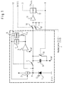
- FIG. 1 Arranged cells in a row or in an array will.
- the cell shown in FIG. 1 has a photodiode 1 trained photosensitive element on the one hand with the earth potential and on the other hand with a current source 2 connected is.
- the potential point P common to the photodiode 1 and the current source 2 is coupled to the input of a controller 3, the output of which is connected to the control input of the current source 2 via two filters 4, 5 connected in parallel, in particular each designed as a low-pass filter, so that the controller 3 ultimately causes the potential point P between the current source 2 and the photodiode 1 to be kept at the potential V ref , which is applied to the second input of the controller 2.
- the first filter 4 has a time constant of 1 kHz and is directly between the output of controller 3 and the control input the power source 2 switched.
- the second filter 5 has a time constant of 50kHz and is also between the output of controller 3 and the control input of Current source 2 switched, but between the output the controller 3 and the input of the filter 5 a controllable Switch 6 is provided.
- the common potential P of the photodiode 1 and the current source 2 is connected via a likewise controllable switch 7 to a pole of a capacitor 8, the other pole of which is at the potential V ref .
- the pole of the switch 7 facing the capacitor 8 is above a further switch 10 with the input of an amplifier 11 coupled, the output of which is the input of a sample and Hold member 12 is supplied.
- the switches 6 and 7 are from a common control input SE applied, i.e. that both switches by the control signal SE can be operated simultaneously, the switch 7 is always open when switch 6 is closed and vice versa.
- switches 10, 10 ', etc. each of which is one in FIG. 1 shown cell is assigned. So if the switches 10, 10 ', etc. can be operated sequentially one after the other sequentially one after the other in the capacitors 8, 8 ', etc. stored values in the sample and hold element shown 12 can be saved.
- Switch 10, 10 ', etc. For sequentially operating the Switch 10, 10 ', etc. is an address and clock line Ad & Cl provided, via which one of the switches 10, 10 ', etc. can be addressed and operated.
- the clock component of the signal Ad & Cl is on as signal Cl the clock input of the sample-and-hold element 12 to clock this accordingly and for timely reading the values stored in the capacitors 8, 8 ', etc. to care.
- a reset line R is provided by means of which on the one hand the switch 9 can be actuated and closed and on the other hand, the sample-and-hold element 12 can be reset.
- the control loop consisting of elements 2-6 is active, filter 5 with the time constant 50 kHz being decisive here.
- the control loop follows rapid changes at the potential point P, which are caused by ambient light via the photodiode 1.
- the control loop explained consequently ensures with a time constant of 50 kHz that the potential point P is kept at the potential V ref regardless of the amplitude and frequency of the ambient light.
- the capacitor 8 is charged to the potential V ref at the switch positions shown in the drawing, ie charge is stored in the capacitor 8.
- the filter 5 is excluded Force set, which means that only the filter 4th is active with a time constant of 1 kHz.
- the one described The control loop thus only follows slow signal changes and causes at the potential point P that before opening the Switch 6 active control only for interference signals with accordingly low frequency is continued.
- the one that takes place immediately before the useful signal reception Closing the switch 7 causes the one through whom Photodiode 1 flowing additional current through the useful light is caused from the capacitor 8 or from the in this capacitor 8 stored charge is obtained.
- the switch is switched on via the signal SE 7 opened again and switch 6 closed.
- the sample and hold element 12 By addressing and loading the switch 10 over the signal Ad & Cl becomes the charge difference mentioned Capacitor 8 via the amplifier 11, the sample and hold element 12 fed where a storage of this difference signal he follows. The one stored in the sample and hold element 12 Value can then be processed in any way.
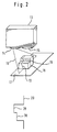
- FIG. 2 shows an optoelectronic sensor arrangement according to the invention 13 housed in a cuboid housing and a transmission optic on one of its long narrow sides 14 and a receiving optics arranged next to this 15 has.
- a light transmitter is provided in the housing behind the transmission optics 14. There is also a behind the receiving optics 15 Light receiver unit with a variety of in a matrix arranged photosensitive elements.
- Light transmitter and transmission optics 14 are designed such that they emit a V-shaped light beam in a plane 16, which extends through the surveillance area towards a level 17 that extends the surveillance area limited on the side facing away from the sensor arrangement 13.
- Level 17 does not necessarily have to be a stationary one, at the end of the monitoring area arranged element, but can also be designed as funding, for example on which objects are transported through the surveillance area will.
- an object 18 which consists of two side by side arranged, different sized cuboids.
- the light beam emitted by the light transmitter is shown in the Embodiment aligned such that it is inclined object 18 hits. It is essential that level 16 of the Transmitting light beam at an angle greater than 0 ° to the optical Axis of the receiving optics 15 runs so that it is also possible would be to hit the transmitted light beam perpendicularly on the object 18 to let and the optical axis of the receiver accordingly to align diagonally.
- the light beam irradiating the object 18 in the manner mentioned creates a light line 19 on the object 18, the so-called Light section.
- this line of light points 19 the course shown in the lower area of FIG. 2 20 on.
- the representation of the course 20 according to FIG. 2 can be seen that this course 20 ultimately the Corresponds to the height profile of the object 18, the area 38 of the course 20 the smaller cuboid of the object 18 and the Area 39 of the course 20 the larger cuboid of the object 18 indicates.
- the height profile in a simple manner using the light section method of an object can be determined, here based on of the principle according to the invention a high level of light immunity is guaranteed.
- the object 18 mentioned in connection with FIG. 2 can also be designed differently.
- it can to be a single object, which has a certain processing state which is recognized according to the invention shall be.
- According to the principle according to the invention e.g. can be recognized whether an object is provided with a milling groove or whether the milling groove has the desired dimensions.
- a typical use case for the detection of multiple objects consists of counting a stream of shingles superimposed newspapers or magazines.
- the difference is made determined from level to level, with fluctuations in the amount of scanned newspapers or magazines that by vibrating the objects transporting said objects Conveyor belts are created by the relative measurement mentioned be compensated.
- relative measurement is used understood that only the stages of the scale flow, i.e. the height differences between two successive, Newspapers or magazines lying on top of each other like shingles be determined.
- FIG. 3 shows a sensor arrangement 21 according to the invention, which like the sensor arrangement 13 according to FIG. 2 in a cuboid Housing is housed.
- the sensor arrangement 21 has an autocollimation optics 22 on which for both the transmit and receive radiation is decisive.
- the sensor arrangement 21 sends a V-shaped light beam 23 towards a reflector 24 which emits the Light reflected back to the sensor arrangement 21.
- the monitoring area is on one side by the reflector 24 and on the other hand through the sensor arrangement 21 limited.
- the band 27 hangs between positions 25 and 26 in such a way that it projects into the area of the light beam 23 and in this way prevents all of light from the sensor arrangement 21 onto the area 28 of the reflector hits. Due to the sagging band 27 strikes only the area 29 of the reflector from the sensor arrangement 21 emitted light, so that even from this area 29 reflects light back to the sensor arrangement 21 becomes.
- the size of the sensor arrangement 21 can of area 29 can be determined, which is ultimately a measure represents for the current sag of the band 27.
- V-shaped described above in connection with Figure 3 Illumination of the band 27 or the reflector 24 can alternatively, advantageously also by means of a telecentric Lighting to be replaced, which essentially only includes light beams directed in parallel.
- the transformation the V-shaped lighting into a telecentric lighting can for example by a concave mirror or a lens can be achieved.
- FIG. 4 shows an optoelectronic sensor arrangement according to the invention 30, which, like the sensor arrangement according to FIG Figures 2 and 3 housed in a cuboid housing is.
- the sensor arrangement 30 sends a light beam 31 in the direction a reflector 32, which the emitted light back to Sensor arrangement 30 reflects.
- the light beam 31 is designed such that the entire area of the reflector 32 is illuminated so that everyone reflective point on the reflector 32 for generation a corresponding signal in the sensor arrangement 30 can lead.
- Photosensitive cells are equipped for differentiation different shades of gray are suitable for example the image of an object according to FIG. 5a on different Types are evaluated:
- 5a has three different bright areas with the area 35 brightest and the area 37 is the darkest.
- the brightness of the area 36 lies between the brightnesses of the two areas 35 and 37.
- a sensor arrangement according to the invention can be programmed in this way or be set so that they only such objects or object areas recognizes which have a brightness that above or below a threshold or between two thresholds lie. This is illustrated by means of FIGS. 5b-d, all from a sensor arrangement according to the invention delivered images of the object according to FIG. 5a show, wherein different operating modes of the sensor arrangement are set.
- An image according to FIG. 5b is delivered, for example, when the sensor arrangement is set such that only those brightness levels of the object lead to image recognition which are below a threshold value S 1 .
- the brightness levels of the object areas 36 and 37 are below the threshold value S 1 , while the brightness of the object area 35 is above this threshold value.
- the ratio of the brightness levels of the areas 35, 36 and 37 to the threshold value S 1 is illustrated by the staircase signal and the threshold value S 1 shown in FIG. 5b.
- the first stage of the staircase signal corresponds to the dark object region 37
- the second stage corresponds to the middle object region 36
- the third stage corresponds to the light object region 35.
- Fig. 5b shows that with the threshold setting mentioned only the object areas 36 and 37 are recognized while reflected from the background and the object area 35 Light does not emit a corresponding light signal leads.
- the image according to FIG. 5b thus only contains the contours of object areas 36 and 37.
- 5c illustrates an operating mode of the sensor according to the invention in which a lower threshold value S 2 is set, so that ultimately only the darkest object area 37 is recognized.
- an operating mode of the sensor according to the invention is also possible in which only those object areas are detected whose brightness lies between the two threshold values S 1 and S 2 .
- the image of the object according to FIG. 5a delivered in such an operating mode is illustrated in FIG. 5d. Only the object area 36 has a brightness that lies between the two threshold values S 1 and S 2 , so that only this object area 36 is also imaged.
Landscapes
- Engineering & Computer Science (AREA)
- Physics & Mathematics (AREA)
- Computer Networks & Wireless Communication (AREA)
- General Physics & Mathematics (AREA)
- Radar, Positioning & Navigation (AREA)
- Remote Sensing (AREA)
- Electromagnetism (AREA)
- Geophysics And Detection Of Objects (AREA)
- Optical Elements Other Than Lenses (AREA)
- Length Measuring Devices By Optical Means (AREA)
- Photo Coupler, Interrupter, Optical-To-Optical Conversion Devices (AREA)
- Optical Radar Systems And Details Thereof (AREA)
Applications Claiming Priority (4)
| Application Number | Priority Date | Filing Date | Title |
|---|---|---|---|
| DE1997118389 DE19718389A1 (de) | 1997-04-30 | 1997-04-30 | Opto-elektronische Sensoranordnung |
| DE19718389 | 1997-04-30 | ||
| DE1997127459 DE19727459A1 (de) | 1997-06-27 | 1997-06-27 | Opto-elektronische Sensoranordnung mit mehreren in einer Zeile oder einem Array angeordneten photoempfindlichen Elementen |
| DE19727459 | 1997-06-27 |
Publications (3)
| Publication Number | Publication Date |
|---|---|
| EP0875771A2 true EP0875771A2 (fr) | 1998-11-04 |
| EP0875771A3 EP0875771A3 (fr) | 1999-11-17 |
| EP0875771B1 EP0875771B1 (fr) | 2004-07-14 |
Family
ID=26036227
Family Applications (1)
| Application Number | Title | Priority Date | Filing Date |
|---|---|---|---|
| EP98107139A Expired - Lifetime EP0875771B1 (fr) | 1997-04-30 | 1998-04-20 | Senseur opto-électronique avec des éléments photosensibles arangés en ligne ou matrice |
Country Status (4)
| Country | Link |
|---|---|
| US (1) | US6097489A (fr) |
| EP (1) | EP0875771B1 (fr) |
| JP (1) | JP4213783B2 (fr) |
| DE (1) | DE59811662D1 (fr) |
Cited By (3)
| Publication number | Priority date | Publication date | Assignee | Title |
|---|---|---|---|---|
| DE10360174A1 (de) * | 2003-12-20 | 2005-07-21 | Leuze Lumiflex Gmbh + Co. Kg | Vorrichtung zur Überwachung eines Erfassungsbereichs an einem Arbeitsmittel |
| DE10360789B4 (de) * | 2003-12-23 | 2007-03-15 | Leuze Lumiflex Gmbh + Co. Kg | Vorrichtung zur Überwachung eines Erfassungsbereichs an einem Arbeitsmittel |
| US8803065B2 (en) | 2010-07-02 | 2014-08-12 | Pantron Instruments Gmbh | Light barrier and method for pulsed operation in which the incidence of extraneous light on the detector can be detected and compensated for |
Families Citing this family (4)
| Publication number | Priority date | Publication date | Assignee | Title |
|---|---|---|---|---|
| BRPI0514958A (pt) * | 2004-09-07 | 2008-07-01 | Petromodel Ehf | aparelho e método para análise de tamanho, forma e angularidade e para análise composicional de partìculas de mineral e rocha |
| DE102005060399A1 (de) * | 2005-12-16 | 2007-06-21 | Sick Ag | Optoelektronische Vorrichtung und Verfahren zum Betreiben einer optoelektronischen Vorrichtung |
| US7783376B2 (en) * | 2006-05-10 | 2010-08-24 | The Boeing Company | Photogrammetric contrasting light for hole recognition |
| DE102008004025B4 (de) * | 2007-02-06 | 2010-08-12 | Leuze Electronic Gmbh & Co Kg | Optischer Sensor |
Citations (5)
| Publication number | Priority date | Publication date | Assignee | Title |
|---|---|---|---|---|
| US4851689A (en) * | 1987-04-15 | 1989-07-25 | Alps Electric Co., Ltd. | Photodetecting circuit |
| US4886976A (en) * | 1988-12-28 | 1989-12-12 | Pitney Bowes Inc. | Driver circuitry for multiple sensors |
| EP0372204A2 (fr) * | 1988-12-02 | 1990-06-13 | Atlas Elektronik Gmbh | Capteur optique de surveillance |
| US5198877A (en) * | 1990-10-15 | 1993-03-30 | Pixsys, Inc. | Method and apparatus for three-dimensional non-contact shape sensing |
| FR2731522A1 (fr) * | 1995-03-06 | 1996-09-13 | Ruiz Ventura Ricardo | Procede et dispositif de telemetre optique et detecteur d'obstacles |
Family Cites Families (10)
| Publication number | Priority date | Publication date | Assignee | Title |
|---|---|---|---|---|
| US4102580A (en) * | 1976-12-29 | 1978-07-25 | Nasa | System for the measurement of ultra-low stray light levels |
| DE2939139A1 (de) * | 1979-09-27 | 1981-04-09 | Agfa-Gevaert Ag, 5090 Leverkusen | Entfernungsmessvorrichtung |
| DE3146506A1 (de) * | 1981-11-24 | 1983-06-01 | Maschinenfabrik Alfred Schmermund Gmbh & Co, 5820 Gevelsberg | Verfahren und pruefgeraet zum pruefen des fuellungsgrades von zigarettenenden |
| CH663464A5 (de) * | 1983-10-19 | 1987-12-15 | Oerlikon Buehrle Ag | Optischer abstandszuender zum messen eines vorgebbaren zielabstandes. |
| DE3627972A1 (de) * | 1986-08-18 | 1988-02-25 | Ifm Int Fluggeraete Motoren | Photoelektrischer taster |
| GB2221294B (en) * | 1988-07-26 | 1993-03-03 | Formula Systems Ltd | Detection circuitry |
| US4920260A (en) * | 1988-08-30 | 1990-04-24 | Msc Technologies, Inc. | Detector system for optical mouse |
| DE4236618A1 (de) * | 1992-10-29 | 1994-05-05 | Hirschmann Richard Gmbh Co | Anordnung zum Verhindern von Fehlalarmen bei Bewegungsmeldern mit einem Infrarot-Detektor |
| IT1263446B (it) * | 1993-06-28 | 1996-08-05 | Gd Spa | Metodo per il controllo ottico per il riempimento di sigarette. |
| GB9426242D0 (en) * | 1994-12-24 | 1995-02-22 | Renishaw Plc | Laser diode for raman spectroscopy |
-
1998
- 1998-04-20 EP EP98107139A patent/EP0875771B1/fr not_active Expired - Lifetime
- 1998-04-20 DE DE59811662T patent/DE59811662D1/de not_active Expired - Lifetime
- 1998-04-28 US US09/069,050 patent/US6097489A/en not_active Expired - Lifetime
- 1998-04-30 JP JP12053798A patent/JP4213783B2/ja not_active Expired - Fee Related
Patent Citations (5)
| Publication number | Priority date | Publication date | Assignee | Title |
|---|---|---|---|---|
| US4851689A (en) * | 1987-04-15 | 1989-07-25 | Alps Electric Co., Ltd. | Photodetecting circuit |
| EP0372204A2 (fr) * | 1988-12-02 | 1990-06-13 | Atlas Elektronik Gmbh | Capteur optique de surveillance |
| US4886976A (en) * | 1988-12-28 | 1989-12-12 | Pitney Bowes Inc. | Driver circuitry for multiple sensors |
| US5198877A (en) * | 1990-10-15 | 1993-03-30 | Pixsys, Inc. | Method and apparatus for three-dimensional non-contact shape sensing |
| FR2731522A1 (fr) * | 1995-03-06 | 1996-09-13 | Ruiz Ventura Ricardo | Procede et dispositif de telemetre optique et detecteur d'obstacles |
Cited By (5)
| Publication number | Priority date | Publication date | Assignee | Title |
|---|---|---|---|---|
| DE10360174A1 (de) * | 2003-12-20 | 2005-07-21 | Leuze Lumiflex Gmbh + Co. Kg | Vorrichtung zur Überwachung eines Erfassungsbereichs an einem Arbeitsmittel |
| DE10360174B4 (de) * | 2003-12-20 | 2007-03-08 | Leuze Lumiflex Gmbh + Co. Kg | Vorrichtung zur Überwachung eines Erfassungsbereichs an einem Arbeitsmittel |
| DE10360789B4 (de) * | 2003-12-23 | 2007-03-15 | Leuze Lumiflex Gmbh + Co. Kg | Vorrichtung zur Überwachung eines Erfassungsbereichs an einem Arbeitsmittel |
| US7412861B2 (en) | 2003-12-23 | 2008-08-19 | Leuze Lumiflex Gmbh & Co., Ltd. | Device for monitoring an area of coverage on a work tool |
| US8803065B2 (en) | 2010-07-02 | 2014-08-12 | Pantron Instruments Gmbh | Light barrier and method for pulsed operation in which the incidence of extraneous light on the detector can be detected and compensated for |
Also Published As
| Publication number | Publication date |
|---|---|
| US6097489A (en) | 2000-08-01 |
| JPH10311703A (ja) | 1998-11-24 |
| JP4213783B2 (ja) | 2009-01-21 |
| EP0875771B1 (fr) | 2004-07-14 |
| DE59811662D1 (de) | 2004-08-19 |
| EP0875771A3 (fr) | 1999-11-17 |
Similar Documents
| Publication | Publication Date | Title |
|---|---|---|
| DE2549457C3 (de) | Elektronische Einrichtung zur Erfassung optisch erkennbarer Fehler | |
| DE3532068C2 (fr) | ||
| EP0360126B2 (fr) | Méthode d'opération d'un détecteur optique de fumée et détecteur de fumée pour la mise en oeuvre de la méthode | |
| DE69515500T2 (de) | Automatische elektrische kamera für etikettenbildaufnahme | |
| EP1816488B1 (fr) | Dispositif optoélectronique et son procédé de fonctionnement | |
| EP1738580B1 (fr) | Dispositif pour surveiller une zone, notamment pour securiser une zone dangereuse d'une installation automatique | |
| EP1158460B1 (fr) | Système et procédé de traitement d'images | |
| EP0892280A2 (fr) | Procédé pour faire fonctionner un dispositif capteur opto-électronique | |
| DE3143007A1 (de) | "verfahren und vorrichtung zum kompensieren der signaldrift bei der behaelterpruefung" | |
| EP1850269B1 (fr) | Procédé et dispositif de balayage | |
| DE2431010B2 (de) | Vorrichtung zum Nachweis von Fremdkörpern und/oder Rissen in lichtdurchlässigen Behältern | |
| EP0875771B1 (fr) | Senseur opto-électronique avec des éléments photosensibles arangés en ligne ou matrice | |
| DE19727459A1 (de) | Opto-elektronische Sensoranordnung mit mehreren in einer Zeile oder einem Array angeordneten photoempfindlichen Elementen | |
| EP0553699A1 (fr) | Dispositif de test pour l'extrémité des cigarettes | |
| DE3602008C2 (fr) | ||
| EP2434311B1 (fr) | Procédé de surveillance optique d'un domaine de surveillance et senseur lumineux à réflexion | |
| EP3528005A1 (fr) | Dispositif de caméra tof destiné à la détection d'erreurs | |
| DE102010014912A1 (de) | Sensor zur Prüfung von Wertdokumenten | |
| EP1498747B1 (fr) | Appareil optoélectronique | |
| DE102020113183B4 (de) | Kamera und Verfahren zur Erfassung von bewegten Objekten | |
| EP0143165B1 (fr) | Senseur de distance pour mesurer la distance d'un objet proche | |
| DE19629396C2 (de) | Reflexionslichttaster | |
| DE10101443B4 (de) | Verfahren zur Ermittlung eines Schnittbildes einer Objektstruktur | |
| EP2887105A1 (fr) | Capteur optoélectrique et procédé de détection d'objets brillants | |
| DE1919879B2 (de) | Vorrichtung zum nachweisen von oberflaechenfehlern |
Legal Events
| Date | Code | Title | Description |
|---|---|---|---|
| PUAI | Public reference made under article 153(3) epc to a published international application that has entered the european phase |
Free format text: ORIGINAL CODE: 0009012 |
|
| AK | Designated contracting states |
Kind code of ref document: A2 Designated state(s): CH DE FR IT LI SE |
|
| AX | Request for extension of the european patent |
Free format text: AL;LT;LV;MK;RO;SI |
|
| PUAL | Search report despatched |
Free format text: ORIGINAL CODE: 0009013 |
|
| AK | Designated contracting states |
Kind code of ref document: A3 Designated state(s): AT BE CH CY DE DK ES FI FR GB GR IE IT LI LU MC NL PT SE |
|
| AX | Request for extension of the european patent |
Free format text: AL;LT;LV;MK;RO;SI |
|
| 17P | Request for examination filed |
Effective date: 20000204 |
|
| AKX | Designation fees paid |
Free format text: CH DE FR IT LI SE |
|
| 17Q | First examination report despatched |
Effective date: 20021113 |
|
| GRAH | Despatch of communication of intention to grant a patent |
Free format text: ORIGINAL CODE: EPIDOS IGRA |
|
| GRAS | Grant fee paid |
Free format text: ORIGINAL CODE: EPIDOSNIGR3 |
|
| GRAA | (expected) grant |
Free format text: ORIGINAL CODE: 0009210 |
|
| AK | Designated contracting states |
Kind code of ref document: B1 Designated state(s): CH DE FR IT LI SE |
|
| REG | Reference to a national code |
Ref country code: CH Ref legal event code: EP |
|
| REF | Corresponds to: |
Ref document number: 59811662 Country of ref document: DE Date of ref document: 20040819 Kind code of ref document: P |
|
| PG25 | Lapsed in a contracting state [announced via postgrant information from national office to epo] |
Ref country code: SE Free format text: LAPSE BECAUSE OF FAILURE TO SUBMIT A TRANSLATION OF THE DESCRIPTION OR TO PAY THE FEE WITHIN THE PRESCRIBED TIME-LIMIT Effective date: 20041014 |
|
| ET | Fr: translation filed | ||
| PLBE | No opposition filed within time limit |
Free format text: ORIGINAL CODE: 0009261 |
|
| STAA | Information on the status of an ep patent application or granted ep patent |
Free format text: STATUS: NO OPPOSITION FILED WITHIN TIME LIMIT |
|
| 26N | No opposition filed |
Effective date: 20050415 |
|
| PGFP | Annual fee paid to national office [announced via postgrant information from national office to epo] |
Ref country code: CH Payment date: 20120423 Year of fee payment: 15 |
|
| PGFP | Annual fee paid to national office [announced via postgrant information from national office to epo] |
Ref country code: FR Payment date: 20120511 Year of fee payment: 15 |
|
| REG | Reference to a national code |
Ref country code: CH Ref legal event code: PL |
|
| PG25 | Lapsed in a contracting state [announced via postgrant information from national office to epo] |
Ref country code: CH Free format text: LAPSE BECAUSE OF NON-PAYMENT OF DUE FEES Effective date: 20130430 Ref country code: LI Free format text: LAPSE BECAUSE OF NON-PAYMENT OF DUE FEES Effective date: 20130430 |
|
| REG | Reference to a national code |
Ref country code: FR Ref legal event code: ST Effective date: 20131231 |
|
| PG25 | Lapsed in a contracting state [announced via postgrant information from national office to epo] |
Ref country code: FR Free format text: LAPSE BECAUSE OF NON-PAYMENT OF DUE FEES Effective date: 20130430 |
|
| PGFP | Annual fee paid to national office [announced via postgrant information from national office to epo] |
Ref country code: IT Payment date: 20140428 Year of fee payment: 17 Ref country code: DE Payment date: 20140422 Year of fee payment: 17 |
|
| REG | Reference to a national code |
Ref country code: DE Ref legal event code: R119 Ref document number: 59811662 Country of ref document: DE |
|
| PG25 | Lapsed in a contracting state [announced via postgrant information from national office to epo] |
Ref country code: IT Free format text: LAPSE BECAUSE OF NON-PAYMENT OF DUE FEES Effective date: 20150420 Ref country code: DE Free format text: LAPSE BECAUSE OF NON-PAYMENT OF DUE FEES Effective date: 20151103 |