EP0872882A2 - Method of fabricating a curved metal-ceramic-substrate - Google Patents
Method of fabricating a curved metal-ceramic-substrate Download PDFInfo
- Publication number
- EP0872882A2 EP0872882A2 EP98105261A EP98105261A EP0872882A2 EP 0872882 A2 EP0872882 A2 EP 0872882A2 EP 98105261 A EP98105261 A EP 98105261A EP 98105261 A EP98105261 A EP 98105261A EP 0872882 A2 EP0872882 A2 EP 0872882A2
- Authority
- EP
- European Patent Office
- Prior art keywords
- temperature
- ceramic
- plate
- curved
- metallization
- Prior art date
- Legal status (The legal status is an assumption and is not a legal conclusion. Google has not performed a legal analysis and makes no representation as to the accuracy of the status listed.)
- Withdrawn
Links
- 239000000758 substrate Substances 0.000 title claims abstract description 64
- 238000004519 manufacturing process Methods 0.000 title claims abstract description 8
- 239000000919 ceramic Substances 0.000 claims abstract description 85
- 238000001465 metallisation Methods 0.000 claims abstract description 57
- 229910052751 metal Inorganic materials 0.000 claims abstract description 28
- 239000002184 metal Substances 0.000 claims abstract description 28
- RYGMFSIKBFXOCR-UHFFFAOYSA-N Copper Chemical compound [Cu] RYGMFSIKBFXOCR-UHFFFAOYSA-N 0.000 claims abstract description 26
- 239000011889 copper foil Substances 0.000 claims abstract description 23
- 238000010438 heat treatment Methods 0.000 claims abstract description 22
- 229910000679 solder Inorganic materials 0.000 claims abstract description 13
- 239000011888 foil Substances 0.000 claims abstract description 11
- 239000010949 copper Substances 0.000 claims abstract description 7
- 229910052802 copper Inorganic materials 0.000 claims abstract description 7
- 239000003779 heat-resistant material Substances 0.000 claims abstract description 4
- 229910052709 silver Inorganic materials 0.000 claims abstract description 3
- 238000000034 method Methods 0.000 claims description 44
- 238000000465 moulding Methods 0.000 claims description 18
- 238000001816 cooling Methods 0.000 claims description 15
- 238000005530 etching Methods 0.000 claims description 12
- 238000010304 firing Methods 0.000 claims description 6
- 239000000463 material Substances 0.000 claims description 6
- HBMJWWWQQXIZIP-UHFFFAOYSA-N silicon carbide Chemical compound [Si+]#[C-] HBMJWWWQQXIZIP-UHFFFAOYSA-N 0.000 claims description 5
- 230000002829 reductive effect Effects 0.000 claims description 4
- 239000012298 atmosphere Substances 0.000 claims description 3
- 238000005516 engineering process Methods 0.000 claims description 3
- TWNQGVIAIRXVLR-UHFFFAOYSA-N oxo(oxoalumanyloxy)alumane Chemical compound O=[Al]O[Al]=O TWNQGVIAIRXVLR-UHFFFAOYSA-N 0.000 claims description 3
- 238000005245 sintering Methods 0.000 claims description 3
- 238000004080 punching Methods 0.000 claims description 2
- 230000000284 resting effect Effects 0.000 claims description 2
- 239000011261 inert gas Substances 0.000 claims 2
- PMHQVHHXPFUNSP-UHFFFAOYSA-M copper(1+);methylsulfanylmethane;bromide Chemical compound Br[Cu].CSC PMHQVHHXPFUNSP-UHFFFAOYSA-M 0.000 claims 1
- 238000005520 cutting process Methods 0.000 claims 1
- 230000001681 protective effect Effects 0.000 claims 1
- 238000002844 melting Methods 0.000 description 7
- 230000008018 melting Effects 0.000 description 7
- 239000011248 coating agent Substances 0.000 description 3
- 238000000576 coating method Methods 0.000 description 3
- QPLDLSVMHZLSFG-UHFFFAOYSA-N Copper oxide Chemical compound [Cu]=O QPLDLSVMHZLSFG-UHFFFAOYSA-N 0.000 description 2
- 239000005751 Copper oxide Substances 0.000 description 2
- QVGXLLKOCUKJST-UHFFFAOYSA-N atomic oxygen Chemical compound [O] QVGXLLKOCUKJST-UHFFFAOYSA-N 0.000 description 2
- 238000005452 bending Methods 0.000 description 2
- 239000003795 chemical substances by application Substances 0.000 description 2
- 239000004020 conductor Substances 0.000 description 2
- 229910000431 copper oxide Inorganic materials 0.000 description 2
- 230000001419 dependent effect Effects 0.000 description 2
- 238000013461 design Methods 0.000 description 2
- 230000005496 eutectics Effects 0.000 description 2
- 230000017525 heat dissipation Effects 0.000 description 2
- 230000000873 masking effect Effects 0.000 description 2
- 239000012299 nitrogen atmosphere Substances 0.000 description 2
- 239000011224 oxide ceramic Substances 0.000 description 2
- 229910052574 oxide ceramic Inorganic materials 0.000 description 2
- 239000001301 oxygen Substances 0.000 description 2
- 229910052760 oxygen Inorganic materials 0.000 description 2
- 239000000843 powder Substances 0.000 description 2
- 229910010271 silicon carbide Inorganic materials 0.000 description 2
- 238000012546 transfer Methods 0.000 description 2
- 239000000853 adhesive Substances 0.000 description 1
- 230000001070 adhesive effect Effects 0.000 description 1
- 239000002131 composite material Substances 0.000 description 1
- 229910052593 corundum Inorganic materials 0.000 description 1
- 239000010431 corundum Substances 0.000 description 1
- 238000011161 development Methods 0.000 description 1
- 230000018109 developmental process Effects 0.000 description 1
- 238000009826 distribution Methods 0.000 description 1
- 230000000694 effects Effects 0.000 description 1
- 230000005489 elastic deformation Effects 0.000 description 1
- 238000012986 modification Methods 0.000 description 1
- 230000004048 modification Effects 0.000 description 1
- 230000001590 oxidative effect Effects 0.000 description 1
- 230000036961 partial effect Effects 0.000 description 1
- 230000002093 peripheral effect Effects 0.000 description 1
- 238000007639 printing Methods 0.000 description 1
- 230000002441 reversible effect Effects 0.000 description 1
- 239000004065 semiconductor Substances 0.000 description 1
- 238000007493 shaping process Methods 0.000 description 1
- 238000005476 soldering Methods 0.000 description 1
- 239000000126 substance Substances 0.000 description 1
Images


Classifications
-
- H—ELECTRICITY
- H01—ELECTRIC ELEMENTS
- H01L—SEMICONDUCTOR DEVICES NOT COVERED BY CLASS H10
- H01L23/00—Details of semiconductor or other solid state devices
- H01L23/12—Mountings, e.g. non-detachable insulating substrates
- H01L23/13—Mountings, e.g. non-detachable insulating substrates characterised by the shape
-
- C—CHEMISTRY; METALLURGY
- C04—CEMENTS; CONCRETE; ARTIFICIAL STONE; CERAMICS; REFRACTORIES
- C04B—LIME, MAGNESIA; SLAG; CEMENTS; COMPOSITIONS THEREOF, e.g. MORTARS, CONCRETE OR LIKE BUILDING MATERIALS; ARTIFICIAL STONE; CERAMICS; REFRACTORIES; TREATMENT OF NATURAL STONE
- C04B37/00—Joining burned ceramic articles with other burned ceramic articles or other articles by heating
- C04B37/001—Joining burned ceramic articles with other burned ceramic articles or other articles by heating directly with other burned ceramic articles
-
- C—CHEMISTRY; METALLURGY
- C04—CEMENTS; CONCRETE; ARTIFICIAL STONE; CERAMICS; REFRACTORIES
- C04B—LIME, MAGNESIA; SLAG; CEMENTS; COMPOSITIONS THEREOF, e.g. MORTARS, CONCRETE OR LIKE BUILDING MATERIALS; ARTIFICIAL STONE; CERAMICS; REFRACTORIES; TREATMENT OF NATURAL STONE
- C04B37/00—Joining burned ceramic articles with other burned ceramic articles or other articles by heating
- C04B37/02—Joining burned ceramic articles with other burned ceramic articles or other articles by heating with metallic articles
- C04B37/021—Joining burned ceramic articles with other burned ceramic articles or other articles by heating with metallic articles in a direct manner, e.g. direct copper bonding [DCB]
-
- C—CHEMISTRY; METALLURGY
- C04—CEMENTS; CONCRETE; ARTIFICIAL STONE; CERAMICS; REFRACTORIES
- C04B—LIME, MAGNESIA; SLAG; CEMENTS; COMPOSITIONS THEREOF, e.g. MORTARS, CONCRETE OR LIKE BUILDING MATERIALS; ARTIFICIAL STONE; CERAMICS; REFRACTORIES; TREATMENT OF NATURAL STONE
- C04B37/00—Joining burned ceramic articles with other burned ceramic articles or other articles by heating
- C04B37/02—Joining burned ceramic articles with other burned ceramic articles or other articles by heating with metallic articles
- C04B37/023—Joining burned ceramic articles with other burned ceramic articles or other articles by heating with metallic articles characterised by the interlayer used
-
- H—ELECTRICITY
- H01—ELECTRIC ELEMENTS
- H01L—SEMICONDUCTOR DEVICES NOT COVERED BY CLASS H10
- H01L21/00—Processes or apparatus adapted for the manufacture or treatment of semiconductor or solid state devices or of parts thereof
- H01L21/02—Manufacture or treatment of semiconductor devices or of parts thereof
- H01L21/04—Manufacture or treatment of semiconductor devices or of parts thereof the devices having potential barriers, e.g. a PN junction, depletion layer or carrier concentration layer
- H01L21/48—Manufacture or treatment of parts, e.g. containers, prior to assembly of the devices, using processes not provided for in a single one of the subgroups H01L21/06 - H01L21/326
- H01L21/4803—Insulating or insulated parts, e.g. mountings, containers, diamond heatsinks
- H01L21/4807—Ceramic parts
-
- H—ELECTRICITY
- H01—ELECTRIC ELEMENTS
- H01L—SEMICONDUCTOR DEVICES NOT COVERED BY CLASS H10
- H01L23/00—Details of semiconductor or other solid state devices
- H01L23/34—Arrangements for cooling, heating, ventilating or temperature compensation ; Temperature sensing arrangements
- H01L23/36—Selection of materials, or shaping, to facilitate cooling or heating, e.g. heatsinks
- H01L23/373—Cooling facilitated by selection of materials for the device or materials for thermal expansion adaptation, e.g. carbon
- H01L23/3735—Laminates or multilayers, e.g. direct bond copper ceramic substrates
-
- H—ELECTRICITY
- H05—ELECTRIC TECHNIQUES NOT OTHERWISE PROVIDED FOR
- H05K—PRINTED CIRCUITS; CASINGS OR CONSTRUCTIONAL DETAILS OF ELECTRIC APPARATUS; MANUFACTURE OF ASSEMBLAGES OF ELECTRICAL COMPONENTS
- H05K3/00—Apparatus or processes for manufacturing printed circuits
- H05K3/0011—Working of insulating substrates or insulating layers
- H05K3/0014—Shaping of the substrate, e.g. by moulding
-
- C—CHEMISTRY; METALLURGY
- C04—CEMENTS; CONCRETE; ARTIFICIAL STONE; CERAMICS; REFRACTORIES
- C04B—LIME, MAGNESIA; SLAG; CEMENTS; COMPOSITIONS THEREOF, e.g. MORTARS, CONCRETE OR LIKE BUILDING MATERIALS; ARTIFICIAL STONE; CERAMICS; REFRACTORIES; TREATMENT OF NATURAL STONE
- C04B2235/00—Aspects relating to ceramic starting mixtures or sintered ceramic products
- C04B2235/65—Aspects relating to heat treatments of ceramic bodies such as green ceramics or pre-sintered ceramics, e.g. burning, sintering or melting processes
- C04B2235/656—Aspects relating to heat treatments of ceramic bodies such as green ceramics or pre-sintered ceramics, e.g. burning, sintering or melting processes characterised by specific heating conditions during heat treatment
- C04B2235/6562—Heating rate
-
- C—CHEMISTRY; METALLURGY
- C04—CEMENTS; CONCRETE; ARTIFICIAL STONE; CERAMICS; REFRACTORIES
- C04B—LIME, MAGNESIA; SLAG; CEMENTS; COMPOSITIONS THEREOF, e.g. MORTARS, CONCRETE OR LIKE BUILDING MATERIALS; ARTIFICIAL STONE; CERAMICS; REFRACTORIES; TREATMENT OF NATURAL STONE
- C04B2235/00—Aspects relating to ceramic starting mixtures or sintered ceramic products
- C04B2235/65—Aspects relating to heat treatments of ceramic bodies such as green ceramics or pre-sintered ceramics, e.g. burning, sintering or melting processes
- C04B2235/656—Aspects relating to heat treatments of ceramic bodies such as green ceramics or pre-sintered ceramics, e.g. burning, sintering or melting processes characterised by specific heating conditions during heat treatment
- C04B2235/6565—Cooling rate
-
- C—CHEMISTRY; METALLURGY
- C04—CEMENTS; CONCRETE; ARTIFICIAL STONE; CERAMICS; REFRACTORIES
- C04B—LIME, MAGNESIA; SLAG; CEMENTS; COMPOSITIONS THEREOF, e.g. MORTARS, CONCRETE OR LIKE BUILDING MATERIALS; ARTIFICIAL STONE; CERAMICS; REFRACTORIES; TREATMENT OF NATURAL STONE
- C04B2237/00—Aspects relating to ceramic laminates or to joining of ceramic articles with other articles by heating
- C04B2237/02—Aspects relating to interlayers, e.g. used to join ceramic articles with other articles by heating
- C04B2237/12—Metallic interlayers
- C04B2237/124—Metallic interlayers based on copper
-
- C—CHEMISTRY; METALLURGY
- C04—CEMENTS; CONCRETE; ARTIFICIAL STONE; CERAMICS; REFRACTORIES
- C04B—LIME, MAGNESIA; SLAG; CEMENTS; COMPOSITIONS THEREOF, e.g. MORTARS, CONCRETE OR LIKE BUILDING MATERIALS; ARTIFICIAL STONE; CERAMICS; REFRACTORIES; TREATMENT OF NATURAL STONE
- C04B2237/00—Aspects relating to ceramic laminates or to joining of ceramic articles with other articles by heating
- C04B2237/30—Composition of layers of ceramic laminates or of ceramic or metallic articles to be joined by heating, e.g. Si substrates
- C04B2237/32—Ceramic
- C04B2237/34—Oxidic
- C04B2237/343—Alumina or aluminates
-
- C—CHEMISTRY; METALLURGY
- C04—CEMENTS; CONCRETE; ARTIFICIAL STONE; CERAMICS; REFRACTORIES
- C04B—LIME, MAGNESIA; SLAG; CEMENTS; COMPOSITIONS THEREOF, e.g. MORTARS, CONCRETE OR LIKE BUILDING MATERIALS; ARTIFICIAL STONE; CERAMICS; REFRACTORIES; TREATMENT OF NATURAL STONE
- C04B2237/00—Aspects relating to ceramic laminates or to joining of ceramic articles with other articles by heating
- C04B2237/30—Composition of layers of ceramic laminates or of ceramic or metallic articles to be joined by heating, e.g. Si substrates
- C04B2237/32—Ceramic
- C04B2237/36—Non-oxidic
- C04B2237/365—Silicon carbide
-
- C—CHEMISTRY; METALLURGY
- C04—CEMENTS; CONCRETE; ARTIFICIAL STONE; CERAMICS; REFRACTORIES
- C04B—LIME, MAGNESIA; SLAG; CEMENTS; COMPOSITIONS THEREOF, e.g. MORTARS, CONCRETE OR LIKE BUILDING MATERIALS; ARTIFICIAL STONE; CERAMICS; REFRACTORIES; TREATMENT OF NATURAL STONE
- C04B2237/00—Aspects relating to ceramic laminates or to joining of ceramic articles with other articles by heating
- C04B2237/30—Composition of layers of ceramic laminates or of ceramic or metallic articles to be joined by heating, e.g. Si substrates
- C04B2237/32—Ceramic
- C04B2237/36—Non-oxidic
- C04B2237/366—Aluminium nitride
-
- C—CHEMISTRY; METALLURGY
- C04—CEMENTS; CONCRETE; ARTIFICIAL STONE; CERAMICS; REFRACTORIES
- C04B—LIME, MAGNESIA; SLAG; CEMENTS; COMPOSITIONS THEREOF, e.g. MORTARS, CONCRETE OR LIKE BUILDING MATERIALS; ARTIFICIAL STONE; CERAMICS; REFRACTORIES; TREATMENT OF NATURAL STONE
- C04B2237/00—Aspects relating to ceramic laminates or to joining of ceramic articles with other articles by heating
- C04B2237/30—Composition of layers of ceramic laminates or of ceramic or metallic articles to be joined by heating, e.g. Si substrates
- C04B2237/40—Metallic
- C04B2237/407—Copper
-
- C—CHEMISTRY; METALLURGY
- C04—CEMENTS; CONCRETE; ARTIFICIAL STONE; CERAMICS; REFRACTORIES
- C04B—LIME, MAGNESIA; SLAG; CEMENTS; COMPOSITIONS THEREOF, e.g. MORTARS, CONCRETE OR LIKE BUILDING MATERIALS; ARTIFICIAL STONE; CERAMICS; REFRACTORIES; TREATMENT OF NATURAL STONE
- C04B2237/00—Aspects relating to ceramic laminates or to joining of ceramic articles with other articles by heating
- C04B2237/50—Processing aspects relating to ceramic laminates or to the joining of ceramic articles with other articles by heating
- C04B2237/54—Oxidising the surface before joining
-
- C—CHEMISTRY; METALLURGY
- C04—CEMENTS; CONCRETE; ARTIFICIAL STONE; CERAMICS; REFRACTORIES
- C04B—LIME, MAGNESIA; SLAG; CEMENTS; COMPOSITIONS THEREOF, e.g. MORTARS, CONCRETE OR LIKE BUILDING MATERIALS; ARTIFICIAL STONE; CERAMICS; REFRACTORIES; TREATMENT OF NATURAL STONE
- C04B2237/00—Aspects relating to ceramic laminates or to joining of ceramic articles with other articles by heating
- C04B2237/50—Processing aspects relating to ceramic laminates or to the joining of ceramic articles with other articles by heating
- C04B2237/70—Forming laminates or joined articles comprising layers of a specific, unusual thickness
-
- C—CHEMISTRY; METALLURGY
- C04—CEMENTS; CONCRETE; ARTIFICIAL STONE; CERAMICS; REFRACTORIES
- C04B—LIME, MAGNESIA; SLAG; CEMENTS; COMPOSITIONS THEREOF, e.g. MORTARS, CONCRETE OR LIKE BUILDING MATERIALS; ARTIFICIAL STONE; CERAMICS; REFRACTORIES; TREATMENT OF NATURAL STONE
- C04B2237/00—Aspects relating to ceramic laminates or to joining of ceramic articles with other articles by heating
- C04B2237/50—Processing aspects relating to ceramic laminates or to the joining of ceramic articles with other articles by heating
- C04B2237/76—Forming laminates or joined articles comprising at least one member in the form other than a sheet or disc, e.g. two tubes or a tube and a sheet or disc
-
- C—CHEMISTRY; METALLURGY
- C04—CEMENTS; CONCRETE; ARTIFICIAL STONE; CERAMICS; REFRACTORIES
- C04B—LIME, MAGNESIA; SLAG; CEMENTS; COMPOSITIONS THEREOF, e.g. MORTARS, CONCRETE OR LIKE BUILDING MATERIALS; ARTIFICIAL STONE; CERAMICS; REFRACTORIES; TREATMENT OF NATURAL STONE
- C04B2237/00—Aspects relating to ceramic laminates or to joining of ceramic articles with other articles by heating
- C04B2237/50—Processing aspects relating to ceramic laminates or to the joining of ceramic articles with other articles by heating
- C04B2237/82—Two substrates not completely covering each other, e.g. two plates in a staggered position
-
- H—ELECTRICITY
- H01—ELECTRIC ELEMENTS
- H01L—SEMICONDUCTOR DEVICES NOT COVERED BY CLASS H10
- H01L2224/00—Indexing scheme for arrangements for connecting or disconnecting semiconductor or solid-state bodies and methods related thereto as covered by H01L24/00
- H01L2224/01—Means for bonding being attached to, or being formed on, the surface to be connected, e.g. chip-to-package, die-attach, "first-level" interconnects; Manufacturing methods related thereto
- H01L2224/42—Wire connectors; Manufacturing methods related thereto
- H01L2224/47—Structure, shape, material or disposition of the wire connectors after the connecting process
- H01L2224/48—Structure, shape, material or disposition of the wire connectors after the connecting process of an individual wire connector
- H01L2224/4805—Shape
- H01L2224/4809—Loop shape
- H01L2224/48091—Arched
-
- H—ELECTRICITY
- H01—ELECTRIC ELEMENTS
- H01L—SEMICONDUCTOR DEVICES NOT COVERED BY CLASS H10
- H01L2224/00—Indexing scheme for arrangements for connecting or disconnecting semiconductor or solid-state bodies and methods related thereto as covered by H01L24/00
- H01L2224/01—Means for bonding being attached to, or being formed on, the surface to be connected, e.g. chip-to-package, die-attach, "first-level" interconnects; Manufacturing methods related thereto
- H01L2224/42—Wire connectors; Manufacturing methods related thereto
- H01L2224/47—Structure, shape, material or disposition of the wire connectors after the connecting process
- H01L2224/48—Structure, shape, material or disposition of the wire connectors after the connecting process of an individual wire connector
- H01L2224/481—Disposition
- H01L2224/48151—Connecting between a semiconductor or solid-state body and an item not being a semiconductor or solid-state body, e.g. chip-to-substrate, chip-to-passive
- H01L2224/48221—Connecting between a semiconductor or solid-state body and an item not being a semiconductor or solid-state body, e.g. chip-to-substrate, chip-to-passive the body and the item being stacked
- H01L2224/48225—Connecting between a semiconductor or solid-state body and an item not being a semiconductor or solid-state body, e.g. chip-to-substrate, chip-to-passive the body and the item being stacked the item being non-metallic, e.g. insulating substrate with or without metallisation
- H01L2224/48227—Connecting between a semiconductor or solid-state body and an item not being a semiconductor or solid-state body, e.g. chip-to-substrate, chip-to-passive the body and the item being stacked the item being non-metallic, e.g. insulating substrate with or without metallisation connecting the wire to a bond pad of the item
-
- H—ELECTRICITY
- H01—ELECTRIC ELEMENTS
- H01L—SEMICONDUCTOR DEVICES NOT COVERED BY CLASS H10
- H01L24/00—Arrangements for connecting or disconnecting semiconductor or solid-state bodies; Methods or apparatus related thereto
- H01L24/01—Means for bonding being attached to, or being formed on, the surface to be connected, e.g. chip-to-package, die-attach, "first-level" interconnects; Manufacturing methods related thereto
- H01L24/42—Wire connectors; Manufacturing methods related thereto
- H01L24/47—Structure, shape, material or disposition of the wire connectors after the connecting process
- H01L24/48—Structure, shape, material or disposition of the wire connectors after the connecting process of an individual wire connector
-
- H—ELECTRICITY
- H01—ELECTRIC ELEMENTS
- H01L—SEMICONDUCTOR DEVICES NOT COVERED BY CLASS H10
- H01L2924/00—Indexing scheme for arrangements or methods for connecting or disconnecting semiconductor or solid-state bodies as covered by H01L24/00
- H01L2924/0001—Technical content checked by a classifier
- H01L2924/00014—Technical content checked by a classifier the subject-matter covered by the group, the symbol of which is combined with the symbol of this group, being disclosed without further technical details
-
- H—ELECTRICITY
- H01—ELECTRIC ELEMENTS
- H01L—SEMICONDUCTOR DEVICES NOT COVERED BY CLASS H10
- H01L2924/00—Indexing scheme for arrangements or methods for connecting or disconnecting semiconductor or solid-state bodies as covered by H01L24/00
- H01L2924/01—Chemical elements
- H01L2924/0102—Calcium [Ca]
-
- H—ELECTRICITY
- H01—ELECTRIC ELEMENTS
- H01L—SEMICONDUCTOR DEVICES NOT COVERED BY CLASS H10
- H01L2924/00—Indexing scheme for arrangements or methods for connecting or disconnecting semiconductor or solid-state bodies as covered by H01L24/00
- H01L2924/01—Chemical elements
- H01L2924/01039—Yttrium [Y]
-
- H—ELECTRICITY
- H01—ELECTRIC ELEMENTS
- H01L—SEMICONDUCTOR DEVICES NOT COVERED BY CLASS H10
- H01L2924/00—Indexing scheme for arrangements or methods for connecting or disconnecting semiconductor or solid-state bodies as covered by H01L24/00
- H01L2924/013—Alloys
- H01L2924/0132—Binary Alloys
- H01L2924/01322—Eutectic Alloys, i.e. obtained by a liquid transforming into two solid phases
-
- H—ELECTRICITY
- H01—ELECTRIC ELEMENTS
- H01L—SEMICONDUCTOR DEVICES NOT COVERED BY CLASS H10
- H01L2924/00—Indexing scheme for arrangements or methods for connecting or disconnecting semiconductor or solid-state bodies as covered by H01L24/00
- H01L2924/095—Indexing scheme for arrangements or methods for connecting or disconnecting semiconductor or solid-state bodies as covered by H01L24/00 with a principal constituent of the material being a combination of two or more materials provided in the groups H01L2924/013 - H01L2924/0715
- H01L2924/097—Glass-ceramics, e.g. devitrified glass
- H01L2924/09701—Low temperature co-fired ceramic [LTCC]
-
- H—ELECTRICITY
- H01—ELECTRIC ELEMENTS
- H01L—SEMICONDUCTOR DEVICES NOT COVERED BY CLASS H10
- H01L2924/00—Indexing scheme for arrangements or methods for connecting or disconnecting semiconductor or solid-state bodies as covered by H01L24/00
- H01L2924/30—Technical effects
- H01L2924/35—Mechanical effects
- H01L2924/351—Thermal stress
- H01L2924/3511—Warping
-
- H—ELECTRICITY
- H05—ELECTRIC TECHNIQUES NOT OTHERWISE PROVIDED FOR
- H05K—PRINTED CIRCUITS; CASINGS OR CONSTRUCTIONAL DETAILS OF ELECTRIC APPARATUS; MANUFACTURE OF ASSEMBLAGES OF ELECTRICAL COMPONENTS
- H05K1/00—Printed circuits
- H05K1/02—Details
- H05K1/03—Use of materials for the substrate
- H05K1/0306—Inorganic insulating substrates, e.g. ceramic, glass
-
- H—ELECTRICITY
- H05—ELECTRIC TECHNIQUES NOT OTHERWISE PROVIDED FOR
- H05K—PRINTED CIRCUITS; CASINGS OR CONSTRUCTIONAL DETAILS OF ELECTRIC APPARATUS; MANUFACTURE OF ASSEMBLAGES OF ELECTRICAL COMPONENTS
- H05K2201/00—Indexing scheme relating to printed circuits covered by H05K1/00
- H05K2201/09—Shape and layout
- H05K2201/09009—Substrate related
- H05K2201/09018—Rigid curved substrate
-
- H—ELECTRICITY
- H05—ELECTRIC TECHNIQUES NOT OTHERWISE PROVIDED FOR
- H05K—PRINTED CIRCUITS; CASINGS OR CONSTRUCTIONAL DETAILS OF ELECTRIC APPARATUS; MANUFACTURE OF ASSEMBLAGES OF ELECTRICAL COMPONENTS
- H05K2203/00—Indexing scheme relating to apparatus or processes for manufacturing printed circuits covered by H05K3/00
- H05K2203/11—Treatments characterised by their effect, e.g. heating, cooling, roughening
- H05K2203/1105—Heating or thermal processing not related to soldering, firing, curing or laminating, e.g. for shaping the substrate or during finish plating
-
- H—ELECTRICITY
- H05—ELECTRIC TECHNIQUES NOT OTHERWISE PROVIDED FOR
- H05K—PRINTED CIRCUITS; CASINGS OR CONSTRUCTIONAL DETAILS OF ELECTRIC APPARATUS; MANUFACTURE OF ASSEMBLAGES OF ELECTRICAL COMPONENTS
- H05K2203/00—Indexing scheme relating to apparatus or processes for manufacturing printed circuits covered by H05K3/00
- H05K2203/30—Details of processes not otherwise provided for in H05K2203/01 - H05K2203/17
- H05K2203/302—Bending a rigid substrate; Breaking rigid substrates by bending
-
- Y—GENERAL TAGGING OF NEW TECHNOLOGICAL DEVELOPMENTS; GENERAL TAGGING OF CROSS-SECTIONAL TECHNOLOGIES SPANNING OVER SEVERAL SECTIONS OF THE IPC; TECHNICAL SUBJECTS COVERED BY FORMER USPC CROSS-REFERENCE ART COLLECTIONS [XRACs] AND DIGESTS
- Y10—TECHNICAL SUBJECTS COVERED BY FORMER USPC
- Y10T—TECHNICAL SUBJECTS COVERED BY FORMER US CLASSIFICATION
- Y10T29/00—Metal working
- Y10T29/49—Method of mechanical manufacture
- Y10T29/49002—Electrical device making
- Y10T29/49117—Conductor or circuit manufacturing
- Y10T29/49124—On flat or curved insulated base, e.g., printed circuit, etc.
- Y10T29/49128—Assembling formed circuit to base
-
- Y—GENERAL TAGGING OF NEW TECHNOLOGICAL DEVELOPMENTS; GENERAL TAGGING OF CROSS-SECTIONAL TECHNOLOGIES SPANNING OVER SEVERAL SECTIONS OF THE IPC; TECHNICAL SUBJECTS COVERED BY FORMER USPC CROSS-REFERENCE ART COLLECTIONS [XRACs] AND DIGESTS
- Y10—TECHNICAL SUBJECTS COVERED BY FORMER USPC
- Y10T—TECHNICAL SUBJECTS COVERED BY FORMER US CLASSIFICATION
- Y10T29/00—Metal working
- Y10T29/49—Method of mechanical manufacture
- Y10T29/49002—Electrical device making
- Y10T29/49117—Conductor or circuit manufacturing
- Y10T29/49124—On flat or curved insulated base, e.g., printed circuit, etc.
- Y10T29/49147—Assembling terminal to base
-
- Y—GENERAL TAGGING OF NEW TECHNOLOGICAL DEVELOPMENTS; GENERAL TAGGING OF CROSS-SECTIONAL TECHNOLOGIES SPANNING OVER SEVERAL SECTIONS OF THE IPC; TECHNICAL SUBJECTS COVERED BY FORMER USPC CROSS-REFERENCE ART COLLECTIONS [XRACs] AND DIGESTS
- Y10—TECHNICAL SUBJECTS COVERED BY FORMER USPC
- Y10T—TECHNICAL SUBJECTS COVERED BY FORMER US CLASSIFICATION
- Y10T29/00—Metal working
- Y10T29/49—Method of mechanical manufacture
- Y10T29/49002—Electrical device making
- Y10T29/49117—Conductor or circuit manufacturing
- Y10T29/49124—On flat or curved insulated base, e.g., printed circuit, etc.
- Y10T29/49155—Manufacturing circuit on or in base
- Y10T29/49158—Manufacturing circuit on or in base with molding of insulated base
Definitions
- the invention relates to a method for producing a curved metal-ceramic substrate for use as a substrate in electrical or electronic Circuits or components according to the preamble of claim 1.
- this layer or this coating forms a eutectic with a melting temperature below the melting temperature of the metal (for example copper), so that it can be connected to one another by laying the foil on the ceramic and by heating all the layers, specifically by melting the metal or copper only in the area of the melting layer or oxide layer.
- a curved substrate and its production are known (EP 0 279 601).
- the metal layer on the concavely curved upper side of the ceramic layer has a significantly greater thickness than the metal layer on the convexly curved underside of the substrate.
- This design is necessary in the known case, since there the curvature of the substrate is to be achieved during cooling after the DCB process, with which the two metallizations are attached to the ceramic layer or ceramic plate. Since the metallization on the upper side has a greater thickness and thus a larger volume, thermally induced stresses on the upper side are greater than on the underside, so that the substrate bulges in the aforementioned manner when it cools.
- the object of the invention is to demonstrate a method with which curved metal-ceramic substrates in particular with the same thickness of the metallizations on the Top and bottom can be easily manufactured. To solve this The object is a method according to claim 1.
- the metal-ceramic substrate produced by the method according to the invention is for suitable and has electrical or electronic power circuits or modules an improved, temperature-independent compared to known curved substrates Heat dissipation.
- the method according to the invention provides, initially from a plan or in essentially plan to manufacture a pre-curved ceramic plate and blank then on this bulging ceramic plate in a further process section To apply metallization.
- the curvature of the substrate or the ceramic layer Due to the curvature of the substrate or the ceramic layer, this is possible in the Use to bend elastically so flat that the substrate due to elastic tension of the ceramic layer tightly and firmly against a surface of heat dissipative metal plate is present, and thereby improved heat dissipation results, especially when using a cooling paste between the substrate and the metal plate.
- the curvature of the substrate thus serves, in particular, for a optimal placement of the underside or the lower metallization of the substrate on e.g. a metal plate and thus the best possible heat transfer between the Substrate and this, for example, a metal plate forming a heat sink guarantee.
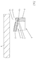
- the substrate 1 shown in the figures consists essentially of a Ceramic layer or ceramic plate 2, for example an aluminum oxide ceramic and that on both surface sides, each with a metallization 3 or 4 is provided.
- the metallizations 3 and 4 are each formed by a copper foil, with the help of the DCB technology known to the person skilled in the art Ceramic layer 2 is connected.
- the metallizations have the same thickness.
- the ceramic layer 2 has a top view rectangular cut with the longer longitudinal axis L and perpendicular to it running shorter transverse axis Q.
- the ceramic layer 2 is in the illustrated Embodiment arched or curved around an axis parallel to the transverse axis, see above that the top of the ceramic layer 2 is concave and the bottom is convex.
- the metallizations 3 and 4 there are curved in the same way.
- the The axis of curvature is indicated by Q 'in FIG. 1, but actually has one much greater distance from the substrate 1 than shown in this figure.
- the Metallization 3 on the top is structured and forms conductor tracks as well Contact surfaces, the latter in particular also for fastening, e.g. for soldering of electronic components 5.
- the metallization 4 on the underside is continuous educated.
- the curvature of the ceramic layer 2 is such that when the substrate with the lower metallization 4 in the middle between the two perpendicular to the longitudinal axis L. and transverse sides 2 'lying parallel to the axis of curvature Q' on a flat surface, for example on the top of a flat metal plate 6, the bottom of the Ceramic layer 2 on each transverse side 2 'a distance x from the top of the Has metal plate 6. In the embodiment shown, this distance is x for example about 0.1-0.8% of the length that the curved ceramic layer 2 between the two sides 2 ', plus the thickness of the lower Metallization 4.
- the thermal conductivity between the substrate 1 and the Metal plate 6, which is part of a heat sink or a housing, for example is, can be significantly improved.
- the substrate 1 is on the top with a layer of a cooling paste 7 provided plate 6 and then on the edge and thus also pressed on the narrow sides 2 'on the plate 6, whereby by the elastic deformation of the ceramic layer 2 a tight fit of the lower Metallization 4 on the metal plate 6 and even distribution of the cooling paste 7 over the entire area occupied by the lower metal coating 4 Metal plate 6 is done.
- the ceramic layer 2 without problems, in particular also can be bent back into a flat shape without the risk of breakage, and even if the top, on the concave side of the ceramic layer provided metallization 3 is structured and thus at least in large part the top of the ceramic layer does not form a continuous metallization, but in the axis direction perpendicular to the axis of curvature only short dimensions having.
- About the upper metallization 3 can thus when bending back Substrate 1 in the flat shape also no excessively high tensile forces between the Ceramic layer 2 and the metallization 3 occur.
- Fig. 3 shows the clamping of the substrate 1 at the edge, i.e. especially in Area of the two narrow sides 2 'on the one forming a rectangular frame Part 8 of a housing 9, with which the substrate 1 then on the part of the heat sink forming plate 6 can be attached using the cooling paste 7.
- the housing part 8 has a fold-like Recess 10, which i.a. a contact surface 11 for supporting the top of the Forms ceramic layer 2 in the region of the edge.
- the fold or contact surface 11, however the underside 12 of the housing part 8 also have a curved course, and in accordance with the curvature of the substrate 1 or the ceramic layer 2.
- the edge or the bottom 12 is on the same level with the bottom of the Metallization 4.
- an intermediate layer 13 made of a permanently elastic mass, preferably one permanently elastic adhesive provided.
- an improved heat transfer between the substrate 1 and the metal plate 6 also has the advantage that stresses between the substrate 1 and the housing 9 are avoided, especially when installing the Substrate 1 on the housing 9. Only when it is attached to the metal plate 6 are the Substrate 1 and the housing 9 elastically deformed.
- Figure 5 Another possible execution is shown in Figure 5. In this version, the upper metallization 3 is sufficient the edge of the ceramic layer 2 and thus lies against the fold surface 11.
- the substrate 1 is curved only about the axis Q '.
- the substrate is also possible to design the substrate so that it is two Axes running perpendicular to each other, namely around the axis Q 'parallel to the Transverse axis Q and at the same time is curved around an axis parallel to the longitudinal axis L, again concave about both axes at the top, so that the substrate for example, a convex on the underside or on the metallization 4 there has a curved surface corresponding to a partial surface of a spherical surface.
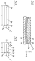
- the substrate was a rectangular cut, i.e. in plan view a rectangular shape having.
- Other shapes are also conceivable for the substrate, for example that in FIG Figure 4 reproduced substrate 14, the shape of which is a rectangular or square green form with protrusions on two opposite sides composed, or the rectangular substrate 15 with rounded and / or chamfered corners and / or the round substrate 16.
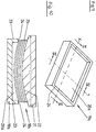
- a molding tool 18 which consists essentially of a sintered or molded plate 19 from a heat-resistant material, for example made of silicon carbide (SiC) and on has a mold cavity or depression 20 on its upper side, which is shown in FIG Embodiment about two mutually perpendicular axes that are parallel to the Longitudinal axis and transverse axis of the mold plate 19 are.
- the longitudinal axis is at the 7 with the X axis and the transverse axis with the Y axis.
- the Depth t of the mold cavity 20 in the direction perpendicular to the X axis and Y axis running Z axis is, for example, 0.05-1.5% of the width of the B or else the Length L.
- the depth t is, for example, 1 mm.
- a separating powder, e.g. corundum powder, is located between the blanks 2a.
- the Plate blanks 2a are, for example, made of a green ceramic extruded or otherwise shaped material made by punching.
- the Dimensions of the blanks 2a are slightly smaller than the dimensions of the mold plate 19.
- the blanks 2a Because of the dead weight of the blanks, they lie against each other and the lowest blank against the surface formed by the mold cavity 20. At a sufficiently high temperature, for example at 1350 ° C, the blanks 2a then sintered or fired in a normal atmosphere so that after the burner arched ceramic plates 2 are obtained.
- the fired ceramic plates 2 are slowly cooled to room temperature, with a cooling rate or a decrease in temperature of about 3 ° C. per minute.
- the individual, curved ceramic plates 2 are removed from the stack and then each provided with the metallizations 3 and 4.
- an oxidized copper foil for example forming the metallization 3, with a thickness of 0.3 mm is placed on one side of each curved ceramic layer 2. This is followed by heating to 1072 ° C in a nitrogen atmosphere with an oxygen content of 35 ppm.
- the curved ceramic plate and the copper foil which is then tightly lying on it and becomes soft due to the heating, but is only molten in the area of the eutectic formed by the copper oxide layer, are used for about six Minutes kept at the temperature of 1072 ° C.
- This is then cooled to room temperature and the metallization is applied to the other surface side of the ceramic plate 2, for example the metallization 4, in the same way.
- the structuring of at least one metallization takes place with the aid of a masking and etching technique, namely for example the metallization 3.
- an etching mask is applied to this metallization.
- the etching then takes place with a suitable etching agent, for example FeCl 3 . After the etching, the etching mask is removed.
- the substrates then produced have metallizations 3 and 4 of the same thickness and for example a bulge of the order of 0.5-6 mm.
- a weight plate 21 is placed on the stack of the blank 2a put on, which are also made of a temperature-resistant material, for example Sintered material, e.g. Silicon carbide (SiC) exists.
- the weight plate forms on the Underside of a surface 22, the shape of the geometry of the shaped surface of the trough 20th corresponds.
- this weight plate 21 is shown so that the Length dimension L 'is approximately the length L of the mold plate, with the Width dimension of the weight plate 21 is approximately the width B of the molding plate 19 corresponds.
- the length L 'and / or the Width B 'of the weight plate 21 deviates from the length L or the width B, i.e. is much smaller or much larger.
- the length L ' in the range between 0.2 - 200% of L.
- the area of the mold trough 20 is curved. Basically, there is also the possibility that the area of a plurality of successive stages is formed.
- the curved or curved ceramic plate 2 is curved around two mutually perpendicular spatial axes. It understands It is evident that substrates are also produced with the method described can be, each one curved around only one spatial axis Have ceramic layer or ceramic plate.
- the trough 20 is concave only about an axial direction, and for example as a cylindrical surface and not as a spherical surface.
- the stack is extended onto a shaped plate which is concave only around an axis the plate blanks 2a and then after complaining with the Weight plate 21 in the manner described above at a sufficient temperature sintered or pre-fired, for example at a temperature of about 1350 ° C. It is then cooled to room temperature and the stack is placed on top from the pre-fired plate blanks 1 'onto a new shaped plate which is similar to the 9 has a mold cavity 20 which e.g. again only by one Axis is concave.
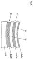
- FIGS. 10-13 show a molding tool 18a and one with this molding tool carried out process for the production of curved ceramic plates 2.
- Das Molding tool 18a consists of a molding plate 19a and a weighting plate 21.
- the mold plate 19a forms on its upper side the concave mold cavity 20a a depression is realized, which has a substantially constant depth t ', by a closed, circumferential edge 23 and a substantially flat Floor is limited.
- the depth t ' is again approximately 0.05-1.5% of the length L or width B.
- the edge 23 forms a mold cavity 20a enclosing edge surface 24 with a constant width b, which is about 0.2-20% in length L or width B corresponds.
- a stack of plate blanks 2b is placed on the molding plate 19a in such a way that the bottom blank 2b rests with its peripheral edge on the edge 23, approximately over a width of 3 mm.
- the stack contains, for example, a total of fifty blanks 2b, each blank 2b having a rectangular cut with a length of 150 mm and a width of 100 mm.
- the blanks 2b are fired flat ceramic plates (Al 2 0 3 96%).
- the weight plate 21 is placed on the stack. Then the stack is on 1200 ° C with a heating rate of about 2 ° C / minute and then about kept at 1200 ° C for five hours. Then it cools down Room temperature with a cooling rate of approx. 2 ° C / minute.
- the cooled ceramic plates then surprisingly have a curvature in two perpendicular spatial axes.
- Process steps the application of the metallizations 3 and 4 namely for example, first the application of the metallization 3 by placing one oxidized copper foil with a thickness of 0.3 mm on the concave curved top the respective pre-curved ceramic plate 2, which is then together with this copper foil in a nitrogen atmosphere with an oxygen content of approx. 35 ppm heated to 1072 ° C and for example for six minutes at this temperature held and then cooled to room temperature.
- the metallization 4 is applied in an analogous manner using an oxidized copper foil. Then at least one of the two metallizations, for example the metallization 3, is structured by means of the masking and etching technique, for which an etching mask is applied and then the etching is carried out with a suitable etching agent, for example with FeCl 3 . The etching mask is then removed.
- a suitable etching agent for example with FeCl 3
- This method can be modified in such a way that the production of the curved ceramic plates 2 takes place in two steps, for example under Use of a molding plate 19a, similar to that of FIG. 12, only on two opposite sides has the upwardly projecting edge 23, so that the Blanks 2b in this first step only with two opposite one another Edge areas rest on the edges 23 and in the first method step only be arched around a spatial axis.
- the blanks are then after the first process step or after the first heat treatment to room temperature cooled and placed on a further molding plate for a second process step, which in turn is similar to the representation of FIG. 13 only on two each other opposite sides has the edge 23, in such a way that the blanks now rest with their other two edge areas on the edges 23.
- the heating rate of, for example, 2 ° C./minute and keeping the Blanks at a temperature of approx. 1200 ° C for a sufficient period of time, for example five hours and then a slow cool down with one Cooling speed from approx. 2 ° C / minute to room temperature.
- the metallizations 3 and 4 can also be applied in other ways, for example by printing the curved ceramic plate 2 with a solder paste, for example with a solder paste consisting of 40% Ag, 55% Cu and 5% Ti both on the top and bottom of the ceramic plate 2.
- a solder paste for example with a solder paste consisting of 40% Ag, 55% Cu and 5% Ti both on the top and bottom of the ceramic plate 2.
- the method step involves contacting the ceramic layer on both sides with one each Copper foil with a thickness of 0.3 mm and then heating the whole Arrange in vacuum at about 850 ° C and hold the array over one sufficient time, for example eight minutes at this temperature. It is then cooled to room temperature. Subsequently, in the Structuring at least one metallization described above respectively.
- the substrates are a Have a bulge of 0.5 - 0.6 mm.
- solder foil is, for example, a thin copper foil which is oxidized on both sides and which is placed between the curved ceramic plate 2 and the copper foil forming the respective metallization the assembly is heated to a temperature of, for example, 1072 ° C.
- the copper foil is connected to the ceramic by melting the solder foil, and the metallization is carried out using the solder foil and the copper foils forming the metallizations can again be made here in two successive steps, firstly on one side, for example for producing the metallization 3, and then for the other side, for example for producing the metallization 4.
- FIG. 14 Another possibility for producing the curved ceramic plates 2 from the Blanks 2a or 2b is shown in FIG. 14.
- a molding plate 19 used, on which a first stack 25 of blanks 2a or 2b is applied.
- a further shaped or sintered plate 26 which is on it Top of the mold surface or mold cavity of the mold plate 19 correspondingly concave is shaped and is correspondingly convex on its underside.
- On this second one Stack 25 a second mold plate 26 is arranged on which a third stack 25 extends Blanks 2a or 2b is located.
- the mold plates 26 in turn consist of the heat-resistant material, namely sintered material, for example silicon carbide.
- Silicon carbide is suitable for the molding plate 19 or 19a and the weighting plate 21 or another material, which by the heat treatment or Burning forces and temperatures are not deformable.
Landscapes
- Engineering & Computer Science (AREA)
- Chemical & Material Sciences (AREA)
- Ceramic Engineering (AREA)
- Microelectronics & Electronic Packaging (AREA)
- Materials Engineering (AREA)
- Condensed Matter Physics & Semiconductors (AREA)
- Computer Hardware Design (AREA)
- General Physics & Mathematics (AREA)
- Power Engineering (AREA)
- Physics & Mathematics (AREA)
- Structural Engineering (AREA)
- Organic Chemistry (AREA)
- Manufacturing & Machinery (AREA)
- Ceramic Products (AREA)
- Cooling Or The Like Of Semiconductors Or Solid State Devices (AREA)
- Structure Of Printed Boards (AREA)
- Laminated Bodies (AREA)
Abstract
Description
Die Erfindung bezieht sich auf ein Verfahren zum Herstellen eines gewölbten Metall-Keramik-Substrats
zur Verwendung als Substrat bei elektrischen oder elektronischen
Schaltkreisen oder Bauelementen gemäß Oberbegriff Patentanspruch 1.The invention relates to a method for producing a curved metal-ceramic substrate
for use as a substrate in electrical or electronic
Circuits or components according to the preamble of
Bekannt ist es, die zum Herstellen von Leiterbahnen, Anschlüssen usw. benötigte
Metallisierung auf einer Keramik, z.B. auf einer Aluminium-Oxid-Keramik mit Hilfe des
sogenannten ![]()
![]()
Dieses DCB-Verfahren weist dann z.B. folgende Verfahrensschritte auf:
- Oxidieren einer Kupferfolie derart, daß sich eine gleichmäßige Kupferoxidschicht ergibt;
- Aufliegen des Kupferfolie auf die Keramikschicht;
- Erhitzen des Verbundes auf eine Prozeßtemperatur zwischen etwa 1065° bis 1085°C, z.B. auf ca. 1071°C;
- Oxidizing a copper foil in such a way that a uniform copper oxide layer results;
- Resting the copper foil on the ceramic layer;
- Heating the composite to a process temperature between about 1065 ° to 1085 ° C, for example to about 1071 ° C;
Bekannt ist ein gewölbtes Substrat und dessen Herstellung (EP 0 279 601). Im
bekannten Fall besitzt die Metallschicht an der konkav gewölbten Oberseite der
Keramikschicht eine deutlich größere Dicke als die Metallschicht an der konvex
gewölbten Unterseite des Substrates. Diese Ausbildung ist im bekannten Fall notwendig,
da dort die Wölbung des Substrates beim Abkühlen nach dem DCB-Prozess erreicht
werden soll, mit dem die beiden Metallisierungen auf der Keramikschicht bzw.
Keramikplatte befestigt werden. Da die Metallisierung an der Oberseite eine größere
Dicke und damit ein größeres Volumen aufweist, sind thermisch bedingte Spannungen
an der Oberseite größer als an der Unterseite, so daß sich das Substrat beim Abkühlen
in der vorgenannten Weise wölbt. Nachteilig ist hierbei u.a., daß dieser
Aufgabe der Erfindung ist es, ein Verfahren aufzuzeigen, mit welchem gewölbte Metall-Keramiksubstrate
insbesondere mit gleicher Dicke der Metallisierungen an der
Oberseite und Unterseite problemlos hergestellt werden können. Zur Lösung dieser
Aufgabe ist ein Verfahren entsprechend dem Patentanspruch 1 ausgebildet.The object of the invention is to demonstrate a method with which curved metal-ceramic substrates
in particular with the same thickness of the metallizations on the
Top and bottom can be easily manufactured. To solve this
The object is a method according to
Das mit dem erfindungsgemäßen Verfahren hergestellte Metall-Keramik-Substrat ist für elektrische oder elektronische Leistungsschaltkreise oder -module geeignet und weist gegenüber bekannten gewölbten Substraten eine verbesserte, temperaturunabhängige Wärmeableitung auf.The metal-ceramic substrate produced by the method according to the invention is for suitable and has electrical or electronic power circuits or modules an improved, temperature-independent compared to known curved substrates Heat dissipation.
Das erfindungsgemäße Verfahren sieht vor, zunächst aus einem planen oder im wesentlichen planen Plattenrohling eine vorgewölbte Keramikplatte herzustellen und dann auf diese vorgewölbte Keramikplatte in einem weiteren Verfahrensabschnitt die Metallisierung aufzubringen. The method according to the invention provides, initially from a plan or in essentially plan to manufacture a pre-curved ceramic plate and blank then on this bulging ceramic plate in a further process section To apply metallization.
Durch die Krümmung des Substrates bzw. der Keramikschicht ist es möglich, dieses im Verwendungsfall elastisch derart eben zu biegen, daß das Substrat aufgrund der elastischen Spannung der Keramikschicht dicht und fest gegen eine Fläche einer Wärme ableitenden Metallplatte anliegt, und sich hierdurch eine verbesserte Wärmeableitung ergibt, insbesondere auch bei Verwendung einer Kühlpaste zwischen dem Substrat und der Metallplatte. Die Wölbung des Substrates dient also insbesondere dazu, eine optimale Anlage der Unterseite bzw. der unteren Metallisierung des Substrates an z.B. einer Metallplatte und damit einen möglichst optimalen Wärmeübergang zwischen dem Substrat und dieser beispielsweise einen Kühlkörper bildenden Metallplatte zu gewährleisten. Dieses durch die Vorkrümmung des Substrates erzielte, verbesserte Verbindung zwischen dem Substrat und der Metallplatte soll unabhängig von der jeweiligen Temperatur des Substrates bzw. der Metallplatte möglichst konstant sein. Diese Forderung ist dann nicht mehr erfüllt, wenn eine der beiden Metallschichten eine größere Dicke aufweist, da eine Metallisierung mit größerer Dicke und damit mit größerem Volumen bei Temperaturänderungen stärkere temperaturbedingte, sich ändernde Spannungen auf die betreffende Oberflächenseite der Keramikschicht ausübt. Unterschiedliche Dicken der beiden Metallisierungen auf der Oberseite und Unterseite würden somit zu einer temperaturabhängigen zusätzlichen Verwölbung des Substrates führen.Due to the curvature of the substrate or the ceramic layer, this is possible in the Use to bend elastically so flat that the substrate due to elastic tension of the ceramic layer tightly and firmly against a surface of heat dissipative metal plate is present, and thereby improved heat dissipation results, especially when using a cooling paste between the substrate and the metal plate. The curvature of the substrate thus serves, in particular, for a optimal placement of the underside or the lower metallization of the substrate on e.g. a metal plate and thus the best possible heat transfer between the Substrate and this, for example, a metal plate forming a heat sink guarantee. This improved by the pre-curvature of the substrate Connection between the substrate and the metal plate should be independent of the respective temperature of the substrate or the metal plate to be as constant as possible. This requirement is no longer met if one of the two metal layers has one has greater thickness, since a metallization with greater thickness and thus with larger volume with temperature changes stronger temperature-related ones exerts changing tensions on the relevant surface side of the ceramic layer. Different thicknesses of the two metallizations on the top and bottom would thus result in a temperature-dependent additional warpage of the substrate to lead.
Bei dem Krümmungsgrad, welches die Erfindung vorsieht, ist auch ein Brechen der Keramikschicht mit Sicherheit vermieden.With the degree of curvature provided by the invention, there is also a breaking of the Certainly avoided ceramic layer.
Weiterbildungen der Erfindung sind Gegenstand der Unteransprüche. Die Erfindung wird im folgenden anhand der Figuren an einem Ausführungsbeispiel näher erläutert. Es zeigen:
- Fig. 1
- in vereinfachter Darstellung und in Seitenansicht ein Substrat gemäß der Erfindung, zusammen mit einer unter dem Substrat angeordneten Metallplatte;
- Fig. 2
- eine Draufsicht auf das Substrat der Fig. 1;
- Fig. 3
- in vergrößerter Detaildarstellung einen Schnitt durch den in einem Gehäuse eingespannten Rand des Substrates;
- Fig. 4
- in Draufsicht verschiedene Formen eines Substrates der Erfindung;
- Fig. 5
- eine ähnliche Darstellung wie Fig. 3, jedoch bei einer weiteren Ausführungsform;
- Fig. 6
- in vereinfachter Darstellung eine Sinter-Form zusammen mit einem Stapel aus Keramikplatten und einer auf diesem Stapel angeordneten Beschwerungsplatte beim Formen bzw. Biegen der Keramikplatten;
- Fig. 7
- in vereinfachter perspektivischer Einzeldarstellung die Form bzw. Sinterplatte;
Figuren 8 und 9- die Form im Längsschnitt (Schnittlinie I-I der Fig. 7) bzw. im Querschnitt (entsprechend der Schnittlinie II-II der Fig. 7);
- Fig. 10
- in einer Darstellung ähnlich wie Fig. 6 eine weitere mögliche Ausführungsform des Formwerkzeuges;
- Fig. 11
- die Sinter- oder Formplatte des Formwerkzeuges der Fig. 6 in perspektivischer Einzeldarstellung;
Figuren 12 und 13- Schnitte entsprechend den Linien III-III bzw. IV-IV der Fig. 11.
- Fig. 1
- in a simplified representation and in side view a substrate according to the invention, together with a metal plate arranged under the substrate;
- Fig. 2
- a plan view of the substrate of Fig. 1;
- Fig. 3
- an enlarged detail view of a section through the edge of the substrate clamped in a housing;
- Fig. 4
- different shapes of a substrate of the invention in plan view;
- Fig. 5
- a representation similar to Figure 3, but in a further embodiment.
- Fig. 6
- in a simplified representation a sintered shape together with a stack of ceramic plates and a weighting plate arranged on this stack when molding or bending the ceramic plates;
- Fig. 7
- the form or sintered plate in a simplified perspective individual representation;
- Figures 8 and 9
- the shape in longitudinal section (section line II of Fig. 7) or in cross section (corresponding to section line II-II of Fig. 7);
- Fig. 10
- in a representation similar to FIG. 6, a further possible embodiment of the molding tool;
- Fig. 11
- the sintered or molded plate of the mold of Figure 6 in a perspective individual representation.
- Figures 12 and 13
- Sections corresponding to lines III-III and IV-IV of FIG. 11.
Das in den Figuren dargestellte Substrat 1 besteht im wesentlichen aus einer
Keramikschicht bzw. Keramikplatte 2, die beispielsweise eine Aluminiumoxid-Keramik
ist und die an beiden Oberflächenseiten mit jeweils einer Metallisierung 3 bzw. 4
versehen ist. Die Metallisierungen 3 und 4 sind jeweils von einer Kupferfolie gebildet,
die mit Hilfe der dem Fachmann bekannten DCB-Technik flächig mit der
Keramikschicht 2 verbunden ist. Die Metalliesierungen besitzen die gleiche Dicke.The
Bei der dargestellten Ausführungsform besitzt die Keramikschicht 2 in Draufsicht einen
rechteckförmigen Zuschnitt mit der längeren Längsachse L und der hierzu senkrecht
verlaufenden kürzeren Querachse Q. Die Keramikschicht 2 ist bei der dargestellten
Ausführungsform um eine Achse parallel zur Querachse gewölbt oder gekrümmt, so
daß die Oberseite der Keramikschicht 2 konkav und die Unterseite konvex ist. In
gleicher Weise sind auch die dortigen Metallisierungen 3 und 4 gewölbt. Die
Krümmungsachse ist in der Fig. 1 mit Q' angedeutet, besitzt aber tatsächlich einen
wesentlich größeren Abstand vom Substrat 1, als in dieser Fig. gezeigt. Die
Metallisierung 3 an der Oberseite ist strukturiert und bildet Leiterbahnen sowie
Kontaktflächen, und zwar letztere insbesondere auch zum Befestigen, z.B. zum Auflöten
von elektronischen Bauteilen 5. Die Metallisierung 4 an der Unterseite ist durchgehend
ausgebildet.In the embodiment shown, the
Die Wölbung der Keramikschicht 2 ist derart, daß dann, wenn das Substrat mit der
unteren Metallisierung 4 in der Mitte zwischen den beiden senkrecht zur Längsachse L
und parallel zur Krümmungsachse Q' liegenden Querseiten 2' auf einer ebenen Fläche,
beispielsweise auf der Oberseite einer ebenen Metallplatte 6 aufliegt, die Unterseite der
Keramikschicht 2 an jeder Querseite 2' einen Abstand x von der Oberseite der
Metallplatte 6 aufweist. Bei der dargestellten Ausführungsform ist dieser Abstand x
beispielsweise etwa 0,1 - 0,8 % derjenigen Länge, die die gewölbte Keramikschicht 2
zwischen den beiden Seiten 2' besitzt, und zwar zzgl. der Dicke der unteren
Metallisierung 4.The curvature of the
Es hat sich gezeigt, daß die thermische Leitfähigkeit zwischen dem Substrat 1 und der
Metallplatte 6, die beispielsweise Bestandteil einer Wärmesenke oder eines Gehäuses
ist, wesentlich verbessert werden kann. Das Substrat 1 wird auf die an ihrer Oberseite
mit einer Schicht aus einer Kühlpaste 7 versehene Platte 6 aufgelegt und dann am Rand
und damit auch an den Schmalseiten 2' auf die Platte 6 gedrückt, womit durch die
elastische Verformung der Keramikschicht 2 ein dichtes Anliegen der unteren
Metallisierung 4 an der Metallplatte 6 und ein gleichmäßiges Verteilen der Kühlpaste 7
über die gesamte von der unteren Metallsierung 4 eingenommene Fläche der
Metallplatte 6 erfolgt.It has been shown that the thermal conductivity between the
Bei einer Krümmung, die im Rahmen der vorstehend genannten Grenzen liegt, ist auf
jeden Fall auch sichergestellt, die Keramikschicht 2 ohne Probleme, insbesondere auch
ohne die Gefahr eines Bruches in eine ebene Form zurückgebogen werden kann, und
zwar auch dann, wenn die obere, an der konkaven Seite der Keramikschicht
vorgesehene Metallisierung 3 strukturiert ist und somit zumindest in einem großen Teil
der Oberseite der Keramikschicht keine durchgehende Metallisierung bildet, sondern in
der Achsrichtung senkrecht zur Krümmungsachse nur jeweils kurze Abmessungen
aufweist. Über die obere Metallisierung 3 können somit beim Rückbiegen des
Substrates 1 in die ebene Form auch keine übermäßig hohen Zugkräfte zwischen der
Keramikschicht 2 und der Metallisierung 3 auftreten.With a curvature that is within the limits mentioned above, is on
in any case also ensured the
Fig. 3 zeigt die Einspannung des Substrates 1 am Rand, d.h. insbesondere auch im
Bereich der beiden Schmalseiten 2' an dem einen rechteckförmigen Rahmen bildenden
Teil 8 eines Gehäuses 9, mit dem das Substrat 1 dann an der den Teil der Wärmesenke
bildenden Platte 6 unter Verwendung der Kühlpaste 7 befestigt werden kann. Zur
Aufnahme des Randes des Substrates 1 besitzt das Gehäuseteil 8 eine falzartige
Ausnehmung 10, die u.a. eine Anlagefläche 11 für die Abstützung der Oberseite der
Keramikschicht 2 im Bereich des Randes bildet. Die Falz- oder Anlagefläche 11, aber
auch die Unterseite 12 des Gehäuseteils 8 besitzen einen gekrümmten Verlauf, und
zwar entsprechend der Wölbung des Substrates 1 bzw. der Keramikschicht 2. Der Rand
bzw. die Unterseite 12 liegt auf dem gleichen Niveau mit der Unterseite der
Metallisierung 4. Zwischen dem Rand der Keramikschicht 2 und der Falzfläche 11 ist
eine Zwischenschicht 13 aus einer dauerelestischen Masse, vorzugsweise aus einem
dauerelastischen Kleber vorgesehen. Zusätzlich zu dem vorstehend bereits
beschriebenen Vorteil eines verbesserten Wärmeübergangs zwischen dem Substrat 1
und der Metallplatte 6 besteht auch der Vorteil, daß Spannungen zwischen dem Substrat
1 und dem Gehäuse 9 vermieden sind, insbesondere auch bei der Montage des
Substrates 1 am Gehäuse 9. Erst beim Befestigen auf der Metallplatte 6 werden das
Substrat 1 und das Gehäuse 9 elastisch verformt. Eine weitere mögliche Ausfführung ist
in der Figur 5 gezeigt. Bei dieser Ausführung reicht die obere Metallisierung 3 bis an
den Rand der Keramikschicht 2 und liegt damit gegen die Falzfläche 11 an.Fig. 3 shows the clamping of the
Vorstehend wurde angenommen, daß das Substrat 1 nur um die Achse Q' gekrümmt ist.
Grundsätzlich ist es aber auch möglich, das Substrat so auszuführen, daß es um zwei
senkrecht zueinander verlaufende Achsen, nämlich um die Achse Q' parallel zur
Querachse Q und zugleich auch um eine Achse parallel zur Längsachse L gekrümmt ist,
und zwar wiederum um beide Achsen konkav an der Oberseite, so daß das Substrat
beispielsweise an der Unterseite bzw. an der dortigen Metallisierung 4 eine konvex
gewölbte Fläche entsprechend einer Teilfläche einer Kugeloberfläche besitzt. It was assumed above that the
Vorstehend wurde weiterhin davon ausgegangen, daß das Substrat einen
rechteckförmigen Zuschnitt, d.h. in Draufsicht eine rechteckförmige Ausbildung
aufweist. Auch andere Formen sind für das Substrat denkbar, beispielsweise das in der
Figur 4 wiedergegebenen Substrat 14, dessen Form sich aus einer rechteckförmigen
oder quadratischen Grunform mit Vorsprüngen an zwei gegenüberliegenden Seiten
zusammensetzt, oder das rechteckförmige Substrat 15 mit abgerundeten und/oder
abgeschrägten Ecken und/oder das runde Substrat 16.Above it was further assumed that the substrate was a
rectangular cut, i.e. in plan view a rectangular shape
having. Other shapes are also conceivable for the substrate, for example that in FIG
Figure 4 reproduced
Nachstehend werden in Zusammenhang mit den Figuren 6 - 13 Verfahren und
Formwerkzeuge beschrieben, mit denen das Verformen bzw. Wölben oder Krümmen
der Keramikplatte 2 insbesondere auch vor dem Aufbringen der die Metallisierungen 3
und 4 bildenden Metall- bzw. Kupferfolien möglich ist.In the following, methods and
Shaping tools are described with which the deformation or arching or curving
the
Bei dem in den Figuren 2 - 9 wiedergegebenen Beispiel wird ein Formwerkzeug 18
verwendet, welches im wesentlichen aus einer Sinter- oder Formplatte 19 aus einem
hitzebeständigen Material, beispielsweise aus Siliciumkarbid (SiC) hergestellt ist und an
ihrer Oberseite eine Formmulde oder -vertiefung 20 aufweist, die bei der dargestellten
Ausführungsform um zwei senkrecht zueinander verlaufende Achsen, die parallel zur
Längsachse und Querachse der Formplatte 19 liegen. Die Längsachse ist bei der
Darstellung der Fig. 7 mit X-Achse und die Querachse mit Y-Achse bezeichnet. Die
Tiefe t der Formmulde 20 in Richtung der senkrecht zur X-Achse und Y-Achse
verlaufenden Z-Achse beträgt beispielsweise 0,05 - 1,5% der Breite der B oder aber der
Länge L. Die Tiefe t beträgt beispielsweise 1 mm. Auf die Formplatte 19 werden
mehrere Plattenrohlinge 2a aus grüner, d.h. noch nicht gebrannter Keramik aufgelegt.
Zwischen den Rohlingen 2a befindet sich ein Trennpulver, z.B Korund-Pulver. Die
Plattenrohlinge 2a sind beispielsweise aus einem die grüne Keramik bildenden
extrudierten oder andersweitig geformten Material durch Ausstanzen hergestellt. Die
Abmessungen der Rohlinge 2a sind etwas kleiner als die Abmessungen der Formplatte
19. Aufgrund des Eigengewichtes der Rohlinge liegen diese gegeneinander an und der
unterste Rohling gegen die von der Formmulde 20 gebildete Fläche. Bei einer
ausreichend hoher Temperatur, beispielsweise bei 1350° C werden die Rohlinge 2a
dann in einer normalen Atmosphäre gesintert bzw. gebrannt, so daß nach dem Brenner
gewölbte Keramikplatten 2 erhalten sind.In the example shown in FIGS. 2-9, a
Die gebrannten Keramikplatten 2 werden auf Raumtemperatur langsam abgekühlt, und
zwar mit einer Kühlgeschwindigkeit oder Temperaturabnahme von etwa 3° C pro
Minute. Nach dem Abkühlen auf Raumtemperatur werden die einzelnen, gewölbten
Keramikplatten2 dem Stapel entnommen und dann anschließend jeweils mit den
Metallisierungen 3 und 4 versehen. Hierfür wird auf eine Seite jeder gewölbten
Keramikschicht 2 auf eine Seite eine beispielsweise die Metallisierung 3 bildende
oxidierte Kupferfolie mit einer Dicke von 0,3 mm aufgelegt. Anschließend erfolgt in
einer Stickstoffatmosphäre mit einem Sauerstoffanteil von 35 ppm ein Erhitzen auf
1072° C. Die gewölbte Keramikplatte und die auf dieser dann dicht aufliegende, durch
das Erhitzen weiche, aber nur im Bereich des von der Kupferoxidschicht gebildeten
Eutektikums schmelzflüssigen Kupferfolie werden für etwa sechs Minuten auf der
Temperatur von 1072° C gehalten. Anschließend erfolgt ein Abkühlen auf
Raumtemperatur und das Aufbringen der Metallisierung auf die andere Oberflächenseite
der Keramikplatte 2, beispielsweise der Metallisierung 4 in der gleichen Weise. Nach
dem Aufbringen der Metallisierung 4 und dem erneuten Abkühlen erfolgt die
Strukturierung wenigstens einer Metallisierung mit Hilfe einer Maskierungs- und
Ätztechnik, nämlich beispielsweise der Metallisierung 3. Hierfür wird auf diese
Metallisierung eine Ätzmaske aufgebracht. Anschließend erfolgt das Ätzen mit einem
geeigneten Ätzmittel, beispielsweise FeCl3. Nach dem Ätzen wird die Ätzmaske
entfernt.The fired
Die dann hergestellten Substrate besitzen Metallisierungen 3 und 4 gleicher Dicke und beispielsweise eine Durchwölbung in der Größenordnung von 0,5 - 6 mm.The substrates then produced have metallizations 3 and 4 of the same thickness and for example a bulge of the order of 0.5-6 mm.
Falls es erforderlich ist, wird auf den Stapel der Rohling 2a eine Beschwerplatte 21
aufgesetzt, die ebenfalls aus einem temperaturfesten Material, beispielsweise
Sintermaterial, z.B. Siliciumkarbid (SiC) besteht. Die Beschwerplatte bildet an der
Unterseite eine Fläche 22, deren Form der Geometrie der Formfläche der Mulde 20
entspricht. In der Fig. 6 ist diese Beschwerplatte 21 so dargestellt, daß der
Längenabmessung L' etwa der Länge L der Formplatte ist, wobei auch die
Breitenabmessung der Beschwerplatte 21 in etwa der Breite B der Formplatte 19
entspricht. Grundsätzlich besteht aber die Möglichkeit, daß die Länge L' und/oder die
Breite B' der Beschwerplatte 21 von der Länge L bzw. der Breite B abweicht, d.h.
wesentlich kleiner oder aber wesentlich größer ist. So kann die Länge L' beispielsweise
im Bereich zwischen 0,2 - 200% von L betragen.If necessary, a
Weiterhin wurde vorstehend davon ausgegangen, daß die Fläche der Formmulde 20
gekrümmt ist. Grundsätzlich besteht aber auch die Möglichkeit, daß die Fläche von
einer Vielzahl von aufeinanderfolgenden Stufen gebildet ist. Vorstehend wurde
weiterhin davon ausgegangen, daß die gekrümmte bzw. gewölbte Keramikplatte 2
jeweils um zwei senkrecht zueinander verlaufende Raumachsen gewölbt ist. Es versteht
sich, daß mit dem beschriebenen Verfahren selbstverständlich auch Substrate hergestellt
werden können, die jeweils eine um lediglich eine Raumachse gewölbte
Keramikschicht oder Keramikplatte besitzen. In diesem Fall wird ein Formwerkzeug
verwendet, dessen Formmulde 20 nur um eine Achsrichtung konkav ausgeführt ist, und
zwar beispielsweise als Zylinderfläche und nicht als Kalottenfläche.Furthermore, it was assumed above that the area of the
Weiterhin besteht auch die Möglichkeit, das vorbeschriebene Verfahren wie folgt zu modifizieren:Furthermore, there is also the possibility of the above-described method as follows modify:
Auf eine Formplatte, die nur um eine Achse konkav ausgeführt ist, wird der Stapel aus
den Plattenrohlingen 2a aufgelegt und dann ggf. nach dem Beschweren mit der
Beschwerplatte 21 in der vorbeschriebenen Weise bei ausreichender Temperatur
gesintert bzw. vorgebrannt, beispielsweise bei einer Temperatur von etwa 1350° C.
Anschließend erfolgt ein Abkühlen auf Raumtemperatur und ein Aufliegen des Stapels
aus den vorgebrannten Plattenrohlingen 1' auf eine neue Formplatte, die ähnlich der
Darstellung der Fig. 9 eine Formmulde 20 aufweist, die z.B. wiederum nur um eine
Achse konkav ausgebildet ist. Nach dem Aufliegen der Rohlinge erfolgt dann in einem
zweiten Brand bei einer Temperatur, die wenigstens um ca. 100° C unter der
maximalen Temperatur des ersten Brandes liegt, ein endgültiges Brennen oder Sintern
der Plattenrohlinge, die an ihrer der Formplatte abgewandten Seite dann mit der
Beschwerplatte 21 beschwert sind. Es hat sich gezeigt, daß sich die vorgebrannten
Plattenrohlinge 2a bei diesem zweiten Brand in die Keramikplatten 2 verformen, die um
zwei senkrecht zueinander verlaufende Achsen gekrümmt sind.The stack is extended onto a shaped plate which is concave only around an axis
the
Nach dem zweiten Brand erfolgt dann wiederum das Abkühlen auf Raumtemperatur und das anschließende Metallisieren der einzelnen Keramikplatten.After the second fire, it is then cooled again to room temperature and then metallizing the individual ceramic plates.
Die Figuren 10 - 13 zeigen ein Formwerkzeug 18a und ein mit diesem Formwerkzeug
durchgeführtes Verfahren zum Herstellen von gewölbten Keramikplatten 2. Das
Formwerkzeug 18a besteht aus einer Formplatte 19a sowie aus der Beschwerplatte 21.
Die Formplatte 19a bildet an ihrer Oberseite die konkave Formmulde 20a, die durch
eine Vertiefung realisiert ist, welche eine wesentliche konstante Tiefe t' besitzt, durch
einen geschlossenen, umlaufenden Rand 23 sowie durch einen im wesentlichen ebenen
Boden begrenzt ist. Die Tiefe t' beträgt wieder etwa 0,05 - 1,5% der Länge L oder Breite
B. Der Rand 23 bildet bei der dargestellten Ausführungsform eine die Formmulde 20a
umschließende Randfläche 24 mit einer konstanten Breite b, die etwa 0,2 - 20% Länge
L oder der Breite B entspricht.FIGS. 10-13 show a
Zum Herstellen der gewölbten dünnen Keramikplatten 2 wird ein Stapel aus
Plattenrohlingen 2b auf die Formplatte 19a derart aufgelegt, daß der unterste Rohling 2b
mit seinem Umfangsrand auf dem Rand 23 aufliegt, und zwar etwa über eine Breite von
3 mm. Der Stapel enthält beispielsweise insgesamt fünfzig Rohlinge 2b, wobei jeder
Rohling 2b einen rechteckförmigen Zuschnitt besitzt mit einer Länge von 150 mm und
einer Breite von 100 mm. Bei den Rohlingen 2b handelt es sich um gebrannte ebene
Keramikplatten (Al203 96%).To produce the curved thin
Auf den Stapel wird die Beschwerplatte 21 aufgelegt. Anschließend wird der Stapel auf
1200° C mit einer Aufheizgeschwindigkeit von ca. 2° C/Minute erhitzt und dann etwa
fünf Stunden bei 1200° C gehalten. Anschließend erfolgt ein Abkühlen auf
Raumtemperatur mit einer Abkühlgeschwindigkeit von ca. 2° C/Minute. Die
abgekühlten Keramikplatten besitzen dann in überraschender Weise eine Wölbung in
zwei senkrecht zueinander verlaufenden Raumachsen. Nun erfolgt in weiteren
Verfahrensschritten das Aufbringen der Metallisierungen 3 und 4, und zwar
beispielsweise zunächst das Aufbringen der Metallisierung 3 durch Auflegen einer
oxidierten Kupferfolie mit einer Dicke von 0,3 mm auf die konkav gewölbte Oberseite
der jeweiligen vorgewölbten Keramikplatte 2, die dann anschließend zusammen mit
dieser Kupferfolie in einer Stickstoffatmosphäre mit einem Sauerstoffanteil von ca. 35
ppm auf 1072° C erhitzt und beispielsweise für sechs Minuten auf dieser Temperatur
gehalten und anschließend auf Raumtemperatur abgekühlt wird.The
In einem nächsten Verfahrensschritt erfolgt in analoger Weise das Aufbringen der
Metallisierung 4 unter Verwendung einer oxidierten Kupferfolie. Anschließend wird
wenigstens eine der beiden Metallisierungen, beispielsweise die Metallisierung 3 mittels
der Maskierungs- und Ätztechnik strukturiert, wozu eine Ätzmaske aufgebracht wird
und anschließend das Ätzen mit einem geeigneten Ätzmittel, beispielsweise mit FeCl3
erfolgt. Anschließend wird die Ätzmaske entfernt.In a next process step, the
Dieses Verfahren kann dahingehend modifiziert werden, daß die Herstellung der
gewölbten Keramikplatten 2 in zwei Schritten erfolgt, und zwar beispielsweise unter
Verwendung einer Formplatte 19a, die ähnlich der Fig. 12 nur an zwei
gegenüberliegenden Seiten den nach oben überstehenden Rand 23 aufweist, so daß die
Rohlinge 2b in diesem ersten Schritt nur mit zwei einander gegenüberliegenden
Randbereichen auf den Rändern 23 aufliegen und in dem ersten Verfahrensschritt
lediglich um eine Raumachse gewölbt werden. Die Rohlinge werden dann nach dem
ersten Verfahrensschritt bzw. nach der ersten Hitzebehandlung auf Raumtemperatur
abgekühlt und für einen zweiten Verfahrensschritt auf eine weitere Formplatte aufgelegt,
die ähnlich der Darstellung der Fig. 13 wiederum nur an zwei einander
gegenüberliegenden Seiten den Rand 23 aufweist, und zwar derart, daß die Rohlinge
nunmehr mit ihren beiden anderen Randbereichen auf den Rändern 23 aufliegen. Auch
in dem zweiten Verfahensschritt bzw. bei der zweiten Hitzebehandlung erfolgt ein
Aufheizen des Stapels aus den Rohlingen 2b auf die Temperatur von ca. 1200° C mit
der Aufheizgeschwindigkeit von beispielsweise 2° C/Minute und ein Halten der
Rohlinge auf der Temperatur von ca. 1200° C über eine ausreichende Zeitdauer,
beispielsweise fünf Stunden und danach ein langsames Abkühlen mit einer
Kühlgeschwindigkeit von ca. 2° C/Minute auf Raumtemperatur.This method can be modified in such a way that the production of the
curved
Das Aufbringen der Metallisierungen 3 und 4 kann auch auf andere Weise erfolgen,
beispielweise durch Bedrucken der gewölbten Keramikplatte 2 mit einer Lötpaste,
beispielsweise mit einer Lötpaste bestehend aus 40% Ag, 55% Cu und 5% Ti sowohl
auf der Ober- und Unterseite der Keramikplatte 2. In einem anschließenden
Verfahrensschritt erfolgt ein beidseitiges Kontaktieren der Keramikschicht mit je einer
Kupferfolie mit einer Dicke von 0,3 mm und dann ein Aufheizen der gesamten
Anordnung im Vakuum auf etwa 850° C und ein Halten der Anordnung über eine
ausreichende Zeitdauer, beispielsweise acht Minuten bei dieser Temperatur.
Anschließend erfolgt ein Abkühlen auf Raumtemperatur. Im Anschluß daran kann in der
vorstehend beschriebenen Weise das Strukturieren zumindest einer Metallisierung
erfolgen.The
Überraschenderweise zeigt sich, daß die Substrate nach diesem Verfahren eine Durchwölbung von 0,5 - 0,6 mm besitzen.Surprisingly, it can be seen that the substrates are a Have a bulge of 0.5 - 0.6 mm.
Das Metallisieren kann weiterhin auch unter Verwendung einer sogenannten
Grundsätzlich besteht weiterhin die Möglichkeit, das Formwerkzeug 18 bzw. die
dortige Formplatte 19 auch für die Rohlinge 2b zu verwenden.Basically, there is still the possibility of the
Eine weitere Möglichkeit zum Herstellen der gewölbten Keramikplatten 2 aus den
Rohlingen 2a oder 2b ist in der Fig. 14 dargestellt. Dort ist eine Formplatte 19
verwendet, auf der ein erster Stapel 25 aus Rohlingen 2a oder 2b aufgebracht ist. Auf
diesen ersten Stapel befindet sich eine weitere Form- oder Sinterplatte 26, die an ihrer
Oberseite der Formfläche oder Formmulde der Formplatte 19 entsprechend konkav
geformt ist und an ihrer Unterseite entsprechend konvex geformt ist. Auf der Formplatte
26 befindet sich ein zweiter Stapel aus Rohlingen 2a oder 2b. Auf diesem zweiten
Stapel 25 ist eine zweite Formplatte 26 angeordnet, auf der sich ein dritter Stapel 25 aus
Rohlingen 2a oder 2b befindet. Die Formplatten 26 bestehen wiederum aus dem
hitzebeständen Material, nämlich Sintermaterial, beispielsweise Siliciumkarbid. Durch
die in der Fig. 14 dargestellte Stapelanordnung kann die Anzahl der in einem
Arbeitsgang hergestellten gewölbten Keramikplatten 2 wesentlich erhöht werden.Another possibility for producing the curved
Für die Formplatte 19 bzw. 19a und die Beschwerplatte 21 eignet sich Siliziumkarbid
oder ein anderes Material, welches durch die bei der Hitzebehandlung bzw. beim
Brennen auftretenden Kräften und Temperaturen nicht verformbar ist.Silicon carbide is suitable for the
Die Erfindung wurde voranstehend an Ausführungsbeispielen beschrieben. Es versteht sich, daß zahlreiche Änderungen sowie Abwandlungen möglich sind, ohne daß dadurch der der Erfindung zugrundeliegende Erfindungsgedanke verlassen wird. The invention has been described above using exemplary embodiments. It understands themselves that numerous changes and modifications are possible without this the inventive idea on which the invention is based is abandoned.
- 11
- SubstratSubstrate
- 22nd
- KeramikschichtCeramic layer
- 2'2 '
- QuerseiteShort side
- 2a, 2b2a, 2b
- Rohlingblank
- 3, 43, 4
- MetallisierungMetallization
- 55
- HalbleiterbauelementSemiconductor device
- 66
- MetallplatteMetal plate
- 77
- KühlpasteCooling paste
- 88th
- GehäuseteilHousing part
- 99
- Gehäusecasing
- 1010th
- GehäusefalzCase rebate
- 1111
- FalzflächeFold surface
- 1212th
- Unterseitebottom
- 1313
- dauerelestische Massepermanently elastic mass
- 14, 15, 1614, 15, 16
- SubstratSubstrate
- 18, 18a18, 18a
- FormwerkzeugMolding tool
- 19, 19a19, 19a
- FormplatteMolded plate
- 20, 20a20, 20a
- FormmuldeMold trough
- 2121
- BeschwerplatteWeight plate
- 2222
- Flächesurface
- 2323
- Randedge
- 2424th
- RandflächeEdge surface
- 2525th
- Stapelstack
- 2626
- FormplatteMolded plate
- L, Q, Q'L, Q, Q '
- Achseaxis
- xx
- Abstanddistance
- yy
- Längelength
Claims (18)
wobei beispielsweise nach dem Herstellen der wenigstens einen gewölbten Keramikplatte (2) auf wenigstens eine Oberflächenseite dieser Keramikplatte eine oxidierte Kupferfolie aufgelegt und anschließend auf eine Temperatur zwischen etwa 1065 und 1085° erhitzt, eine vorgegebene Zeitperiode auf dieser Temperatur gehalten und die Anordnung anschließend auf Raumtemperatur abgekühlt wird, und/oder
wobei nach dem Aufbringen der Metallisierung mit Hilfe des DCB-Verfahrens auf die Oberflächenseite, beispielsweise auf die konkav gekrümmte Oberflächenseite und nach dem Abkühlen auf Raumtemperatur auf die andere Oberflächenseite eine weitere oxidierte Kupferfolie aufgelegt und die Anordnung anschließend erneut auf 1065 - 1085° C erhitzt und anschließend abgekühlt wird.Method according to one of the preceding claims, characterized in that the metallization is applied using metal foils forming the metallization, in particular copper foils, using the DCB technique,
where, for example, after the at least one curved ceramic plate (2) has been produced, an oxidized copper foil is placed on at least one surface side of this ceramic plate and then heated to a temperature between approximately 1065 and 1085 °, maintained at this temperature for a predetermined period of time and the arrangement subsequently cooled to room temperature will, and / or
after applying the metallization using the DCB process on the surface side, for example on the concavely curved surface side and after cooling to room temperature, another oxidized copper foil is placed on the surface and the assembly is then heated again to 1065 - 1085 ° C and is then cooled.
und/oder
daß zum Herstellen der Metallisierung an wenigstens einer Oberflächenseite der vorgewölbten Keramikplatte eine Metallschicht und zwischen dieser und der Keramik eine Lötfolie, vorzugsweise in Form einer dünnen oxidierten Kupferfolie, beispielsweise mit einer Dicke von 0,15 - 1,0 mm, vorgesehen wird, und daß anschließend die Anordnung beispielsweise im Vakuum oder in einer Edelgas-Schutzatmosphäre auf eine das Aufschmelzen der Lötfolie bewirkende Temperatur, beispielsweise auf eine Temperatur von ca. 1065 - 1085° C erhitzt wird.Method according to one of the preceding claims, characterized in that a solder paste, preferably in the form of an active solder, for example in the composition of about 40% Ag, 55% Cu and 5% Ti, is used to produce the metallization on at least one surface side of the bulging ceramic plate is provided between a metal foil and the ceramic, and that the arrangement is then preferably heated in a vacuum or in an inert gas atmosphere to at least the liquidus temperature of the solder, preferably to about 750-1000 ° C.
and or
that a metal layer is provided on at least one surface side of the bulging ceramic plate and a solder foil, preferably in the form of a thin oxidized copper foil, for example with a thickness of 0.15-1.0 mm, is provided between the bulging ceramic plate and that the arrangement is then heated, for example in a vacuum or in an inert gas protective atmosphere, to a temperature which causes the solder foil to melt, for example to a temperature of approximately 1065-1085 ° C.
wobei beispielsweise der wenigstens eine Plattenrohling (2a) z.B. durch Ausstanzen und Ablängen hergestellt wird und anschließend der wenigstens eine so gefertigte Plattenrohling (2a) auf das Formelement (19, 19a) aufgelegt und auf eine Sinter- oder Brenntemperatur erhitzt wird (erstes Brennen), und/oder
wobei beispielsweise nach dem ersten Brennen ein Abkühlen auf Raumtemperatur und ein anschließendes Aufliegen des wenigstens einen vorgebrannten Rohlings (2a) auf ein zweites Formelement und dann ein zweites Brennen bei einer reduzierten Temperatur, beispielsweise bei einer um ca. 100° C reduzierten Temperatur erfolgt, und/oder
wobei beispielsweise das erste Brennen bei einer Temperatur höher als 1500° C, vorzugsweise bei einer Temperatur von 1650° C erfolgt.Method according to one of the preceding claims, characterized by the use of a blank (2a) made of a green sheet made of non-fired ceramic,
wherein, for example, the at least one plate blank (2a) is produced, for example, by punching and cutting to length, and then the at least one plate blank (2a) produced in this way is placed on the shaped element (19, 19a) and heated to a sintering or firing temperature (first firing), and or
wherein, for example, after the first firing, cooling to room temperature and subsequent resting of the at least one pre-fired blank (2a) on a second shaped element and then a second firing at a reduced temperature, for example at a temperature reduced by approximately 100 ° C., and /or
for example, the first firing takes place at a temperature higher than 1500 ° C., preferably at a temperature of 1650 ° C.
wobei vorzugsweise zur Bildung der vorgewölbten Keramikplatte der vorgebrannte Plattenrohling auf das Formelement (19, 19a) aufgelegt und dann auf eine Temperatur unterhalb der Sintertemperatur von Keramik, beispielsweise auf eine Temperatur von 1200° C aufgeheizt und eine vorgegebene Zeitdauer auf dieser Temperatur gehalten und anschließend auf Raumtemperatur abgekühlt wird, und/oder
wobei das Aufheizen auf die Behandlungstemperatur mit einer Aufheizgeschwindigkeit bzw. Temperaturzunahme von 2° C/Minute erfolgt und/oder der Rohling über eine Zeitdauer von etwa fünf Stunden auf der Behandlungstemperatur gehalten wird und/oder das Abkühlen auf Raumtemperatur mit einer Abkühlrate bzw. Temperaturreduzierung von 3° C/Minute erfolgt.Method according to one of the preceding claims, characterized by the use of a blank (2a) made of a fired or pre-fired ceramic,
wherein preferably to form the bulging ceramic plate, the pre-fired plate blank is placed on the shaped element (19, 19a) and then heated to a temperature below the sintering temperature of ceramic, for example to a temperature of 1200 ° C. and held at this temperature for a predetermined period of time and then on Room temperature is cooled, and / or
wherein the heating to the treatment temperature is carried out with a heating rate or temperature increase of 2 ° C./minute and / or the blank is held at the treatment temperature for a period of about five hours and / or the cooling to room temperature with a cooling rate or temperature reduction of 3 ° C / minute.
Applications Claiming Priority (2)
| Application Number | Priority Date | Filing Date | Title |
|---|---|---|---|
| DE19715540 | 1997-04-15 | ||
| DE19715540A DE19715540C2 (en) | 1997-04-15 | 1997-04-15 | Method of manufacturing a domed metal-ceramic substrate |
Publications (2)
| Publication Number | Publication Date |
|---|---|
| EP0872882A2 true EP0872882A2 (en) | 1998-10-21 |
| EP0872882A3 EP0872882A3 (en) | 1999-04-21 |
Family
ID=7826465
Family Applications (1)
| Application Number | Title | Priority Date | Filing Date |
|---|---|---|---|
| EP98105261A Withdrawn EP0872882A3 (en) | 1997-04-15 | 1998-03-24 | Method of fabricating a curved metal-ceramic-substrate |
Country Status (3)
| Country | Link |
|---|---|
| US (1) | US6345437B1 (en) |
| EP (1) | EP0872882A3 (en) |
| DE (1) | DE19715540C2 (en) |
Cited By (2)
| Publication number | Priority date | Publication date | Assignee | Title |
|---|---|---|---|---|
| CN103339723A (en) * | 2011-02-08 | 2013-10-02 | 富士电机株式会社 | Method for manufacturing heat dissipating plate for semiconductor module, said heat dissipating plate, and semiconductor module using said heat dissipating plate |
| EP3177580A1 (en) * | 2014-08-05 | 2017-06-14 | Heraeus Deutschland GmbH & Co. KG | Method for producing double-sided metallised ceramic substrates |
Families Citing this family (8)
| Publication number | Priority date | Publication date | Assignee | Title |
|---|---|---|---|---|
| DE19942915A1 (en) * | 1999-09-08 | 2001-03-15 | Still Gmbh | Power semiconductor module |
| JP4692708B2 (en) | 2002-03-15 | 2011-06-01 | Dowaメタルテック株式会社 | Ceramic circuit board and power module |
| GB0805021D0 (en) * | 2008-03-18 | 2008-04-16 | Renishaw Plc | Apparatus and method for electronic circuit manufacture |
| CN102355798B (en) * | 2011-10-25 | 2014-04-23 | 中国兵器工业集团第二一四研究所苏州研发中心 | Manufacturing method of cylindrical module circuit board and sintering bracket |
| CN103794571B (en) * | 2014-01-25 | 2017-01-04 | 嘉兴斯达半导体股份有限公司 | A kind of power semiconductor novel metal-ceramic insulation substrate |
| JP6361532B2 (en) * | 2015-03-10 | 2018-07-25 | 三菱マテリアル株式会社 | Manufacturing method of power module substrate with heat sink |
| KR101953433B1 (en) * | 2016-03-07 | 2019-02-28 | 주식회사 케이씨씨 | apparatus set for producing warpage of ceramic substrate and method for producing warpage of ceramic substrate using there of |
| US11764077B2 (en) * | 2021-07-23 | 2023-09-19 | Innolux Corporation | Composite layer circuit element and manufacturing method thereof |
Citations (4)
| Publication number | Priority date | Publication date | Assignee | Title |
|---|---|---|---|---|
| EP0163548A2 (en) * | 1984-05-31 | 1985-12-04 | Fujitsu Limited | Method for producing multilayer ceramic circuit board |
| GB2255451A (en) * | 1991-05-03 | 1992-11-04 | Marconi Gec Ltd | Ceramic three dimensional electronic structures |
| DE4233073A1 (en) * | 1992-10-01 | 1994-04-07 | Siemens Ag | Semiconductor modular structure prodn. - by convexly shaping and bonding in single hot pressing operation |
| DE19615481A1 (en) * | 1996-04-03 | 1997-10-09 | Schulz Harder Juergen | Metallised ceramic electrical or electronic substrate - has convex curvature for elastic bending into tight contact with heat sink |
Family Cites Families (8)
| Publication number | Priority date | Publication date | Assignee | Title |
|---|---|---|---|---|
| US3766634A (en) * | 1972-04-20 | 1973-10-23 | Gen Electric | Method of direct bonding metals to non-metallic substrates |
| US3744120A (en) * | 1972-04-20 | 1973-07-10 | Gen Electric | Direct bonding of metals with a metal-gas eutectic |
| US4346512A (en) * | 1980-05-05 | 1982-08-31 | Raytheon Company | Integrated circuit manufacturing method |
| JPS57118077A (en) * | 1981-01-06 | 1982-07-22 | Central Glass Co Ltd | Manufacture of glazed ceramic substrate |
| US5236786A (en) * | 1986-05-08 | 1993-08-17 | Lanxide Technology Company, Lp | Shaped ceramic composites with a barrier |
| GB2201123B (en) * | 1987-02-19 | 1990-11-14 | Marconi Electronic Devices | Electrical conductor arrangement |
| US5209798A (en) * | 1991-11-22 | 1993-05-11 | Grunman Aerospace Corporation | Method of forming a precisely spaced stack of substrate layers |
| EP0805492B1 (en) * | 1996-04-03 | 2004-06-30 | Jürgen Dr.-Ing. Schulz-Harder | Curved metal ceramic substrate |
-
1997
- 1997-04-15 DE DE19715540A patent/DE19715540C2/en not_active Expired - Fee Related
-
1998
- 1998-03-24 EP EP98105261A patent/EP0872882A3/en not_active Withdrawn
- 1998-04-07 US US09/055,881 patent/US6345437B1/en not_active Expired - Lifetime
Patent Citations (4)
| Publication number | Priority date | Publication date | Assignee | Title |
|---|---|---|---|---|
| EP0163548A2 (en) * | 1984-05-31 | 1985-12-04 | Fujitsu Limited | Method for producing multilayer ceramic circuit board |
| GB2255451A (en) * | 1991-05-03 | 1992-11-04 | Marconi Gec Ltd | Ceramic three dimensional electronic structures |
| DE4233073A1 (en) * | 1992-10-01 | 1994-04-07 | Siemens Ag | Semiconductor modular structure prodn. - by convexly shaping and bonding in single hot pressing operation |
| DE19615481A1 (en) * | 1996-04-03 | 1997-10-09 | Schulz Harder Juergen | Metallised ceramic electrical or electronic substrate - has convex curvature for elastic bending into tight contact with heat sink |
Cited By (3)
| Publication number | Priority date | Publication date | Assignee | Title |
|---|---|---|---|---|
| CN103339723A (en) * | 2011-02-08 | 2013-10-02 | 富士电机株式会社 | Method for manufacturing heat dissipating plate for semiconductor module, said heat dissipating plate, and semiconductor module using said heat dissipating plate |
| CN103339723B (en) * | 2011-02-08 | 2016-03-09 | 富士电机株式会社 | The manufacture method of semiconductor module heating panel, this heating panel and use the semiconductor module of this heating panel |
| EP3177580A1 (en) * | 2014-08-05 | 2017-06-14 | Heraeus Deutschland GmbH & Co. KG | Method for producing double-sided metallised ceramic substrates |
Also Published As
| Publication number | Publication date |
|---|---|
| US6345437B1 (en) | 2002-02-12 |
| DE19715540A1 (en) | 1998-10-22 |
| EP0872882A3 (en) | 1999-04-21 |
| DE19715540C2 (en) | 2002-02-07 |
Similar Documents
| Publication | Publication Date | Title |
|---|---|---|
| EP1061783B1 (en) | Ceramic-metal substrate, particularly multiple substrate | |
| DE68917259T2 (en) | Heater with positive temperature coefficient and method of manufacturing the same. | |
| EP0650189B1 (en) | Method of manufacture of a semiconductor module | |
| EP0627760B1 (en) | Subdivisible substrate and method of making the same | |
| DE69217285T2 (en) | Ceramic circuit board | |
| EP0805492B1 (en) | Curved metal ceramic substrate | |
| DE69028378T2 (en) | Process for the production of a heat-conducting mixed material | |
| DE3855854T2 (en) | Ceramic-metal composite and process for its manufacture | |
| DE19715540C2 (en) | Method of manufacturing a domed metal-ceramic substrate | |
| EP1459378A2 (en) | Cooling device for a chip and method for production thereof | |
| DE102020119208A1 (en) | Method for producing a metal-ceramic substrate and metal-ceramic substrate produced by such a method | |
| WO2005081371A2 (en) | Method for the production of stacks of plates, especially coolers or cooler elements composed of stacks of plates | |
| EP0632684B1 (en) | Process for manufacturing metal-ceramic substrate | |
| EP0407905A2 (en) | Flat body, in particular for application as a heat sink for electronic power components | |
| DE19615481C5 (en) | Arched metal-ceramic substrate | |
| EP0322434B1 (en) | Flat bodies, in particular for use as heat sinks for electronic power components | |
| DE2249209B2 (en) | LADDER FRAME FOR USE IN ENCLOSURES FOR SEMICONDUCTOR COMPONENTS | |
| DE19614501A1 (en) | Ceramic-metal substrate with differential thermal expansion compensation | |
| DE102021105520B4 (en) | Metal-ceramic substrate and method of manufacturing a metal-ceramic substrate | |
| EP4103351B1 (en) | Lead-free solder foil | |
| DE102012104903B4 (en) | Process for producing metal-ceramic substrates and metal-ceramic substrate produced by this process | |
| EP0696160A2 (en) | Cooling device for electrical or electronic components having a main board and cooling elements, and method for making the same | |
| EP0393496A2 (en) | Substrate for electrical circuit board consisting of copper- and ceramic layers | |
| DE102021126529A1 (en) | Process for producing metal-ceramic substrates and metal-ceramic substrate produced by such a process | |
| WO2022152788A1 (en) | Process for producing a metal-ceramic substrate and metal-ceramic substrate produced using such a process |
Legal Events
| Date | Code | Title | Description |
|---|---|---|---|
| PUAI | Public reference made under article 153(3) epc to a published international application that has entered the european phase |
Free format text: ORIGINAL CODE: 0009012 |
|
| AK | Designated contracting states |
Kind code of ref document: A2 Designated state(s): AT DE FR GB IT |
|
| AX | Request for extension of the european patent |
Free format text: AL;LT;LV;MK;RO;SI |
|
| PUAL | Search report despatched |
Free format text: ORIGINAL CODE: 0009013 |
|
| AK | Designated contracting states |
Kind code of ref document: A3 Designated state(s): AT BE CH DE DK ES FI FR GB GR IE IT LI LU MC NL PT SE |
|
| AX | Request for extension of the european patent |
Free format text: AL;LT;LV;MK;RO;SI |
|
| 17P | Request for examination filed |
Effective date: 19990812 |
|
| AKX | Designation fees paid |
Free format text: AT DE FR GB IT |
|
| STAA | Information on the status of an ep patent application or granted ep patent |
Free format text: STATUS: THE APPLICATION IS DEEMED TO BE WITHDRAWN |
|
| 18D | Application deemed to be withdrawn |
Effective date: 20051004 |