The present invention relates to plasma generators, and more particularly, to a
method and apparatus for generating a plasma to sputter deposit a layer of material in
the fabrication of semiconductor devices.
Low density plasmas have become convenient sources of energetic ions and
activated atoms which can be employed in a variety of semiconductor device
fabrication processes including surface treatments, depositions, and etching
processes. For example, to deposit materials onto a semiconductor wafer using a
sputter deposition process, a plasma is produced in the vicinity of a sputter target
material which is negatively biased. Ions created adjacent to the target impact the
surface of the target to dislodge, i.e., "sputter" material from the target. The sputtered
materials are then transported and deposited on the surface of the semiconductor
wafer.
Sputtered material has a tendency to travel in straight line paths from the target
to the substrate being deposited, at angles which are oblique to the surface of the
substrate. As a consequence, materials deposited in etched trenches and holes of
semiconductor devices having trenches or holes with a high depth to width aspect ratio,
can bridge over causing undesirable cavities in the deposition layer. To prevent such
cavities, the sputtered material can be redirected into substantially vertical paths
between the target and the substrate by negatively charging the substrate to position
vertically oriented electric fields adjacent the substrate if the sputtered material is
sufficiently ionized by the plasma. However, material sputtered in a low density plasma
often has an ionization degree of less than 1% which is usually insufficient to avoid the
formation of an excessive number of cavities. Accordingly, it is desirable to increase the
density of the plasma to increase the ionization rate of the sputtered material in order to
decrease the formation of unwanted cavities in the deposition layer. As used herein,
the term "dense plasma" is intended to refer to one that has a high electron and ion
density.
There are several known techniques for exciting a plasma with RF fields
including capacitive coupling, inductive coupling and wave heating. In a standard
inductively coupled plasma (ICP) generator, RF current passing through a coil
surrounding the plasma induces electromagnetic currents in the plasma. These
currents heat the conducting plasma by ohmic heating, so that it is sustained in steady
state. As shown in U.S. Pat. No. 4,362,632, for example, current through a coil is
supplied by an RF generator coupled to the coil through an impedance-matching
network, such that the coil acts as the first windings of a transformer. The plasma acts
as a single turn second winding of a transformer.
In a number of deposition chambers such as a physical vapor deposition
chamber, the chamber walls are often formed of a conductive metal such as stainless
steel. Because of the conductivity of the chamber walls, it is often necessary to place
the antenna coils or electrodes within the chamber itself because the conducting
chamber walls would block or substantially attenuate the electromagnetic energy
radiating from the antenna. As a result, the coil and its supporting structures are
directly exposed to the deposition flux and energetic plasma particles. This is a
potential source of contamination of the film deposited on the wafer, and is undesirable.
To protect the coils, shields made from nonconducting materials, such as
ceramics, can be placed in front of the coil. However, many deposition processes
involve deposition of conductive materials such as aluminum on the electronic device
being fabricated. Because the conductive material will coat the ceramic shield, it will
soon become conducting, thus again substantially attenuating penetration of
electromagnetic radiation into the plasma. Consequently, it is preferred to place a
shield wall behind the coil to protect the interior of the deposition chamber from the
deposition material. However, the problem of particulate matter remains for sputtering
chambers of this design.
It is an object of the present invention to
provide an improved method and apparatus for
generating a plasma within a chamber and for sputter-depositing
a layer which obviate, for practical
purposes, the above-mentioned limitations.
These and other objects and advantages are
achieved by, in accordance with, one preferred aspect
of the invention, a plasma-generating apparatus which
comprises at least one electron source which injects
energetic electrons into a semiconductor fabrication
chamber to initiate and sustain a relatively high
density plasma at extremely low pressures. In
addition to ionizing atoms of the extremely low
pressure precursor gas, such as an argon gas at 100
microTorr, for example, the energetic electrons are
also believed to collide with target material atoms
sputtered from a target positioned above a substrate,
thereby ionizing the target material atoms and losing
energy as a result of the collisions. As a
consequence, coils or other structures for inductively
coupling RF power to sustain a plasma can be
eliminated.
Preferably, the electrons are injected by
electron guns positioned to inject the electrons
substantially tangentially to the walls of a chamber
shield surrounding the high density plasma into a
confining magnetic field. The magnetic field is
preferably oriented generally parallel to a central
axis of the semi-conductor fabrication chamber and
substantially perpendicular to the surface of the
substrate. As the injected electrons lose energy,
colliding with and ionizing the target material atoms,
and atoms of the extremely low pressure precursor gas,
the electrons spiral inward toward a central region of
the semi-conductor fabrication chamber surrounding the
central axis, forming an electron cloud in the central
region. An arrangement of electromagnetics may be
positioned adjacent the walls of the chamber shield
surrounding the high density plasma to generate the
confining magnetic field. It is believed that the
configuration of confining magnetic fields also keeps
electrons from colliding with the walls of the chamber
shield surrounding the high density plasma.
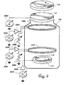
Fig. 1 is a perspective, partial cross-sectional view of a plasma-generating
chamber in accordance with an embodiment of the present invention.
Fig. 2 is a partial cross-sectional view of the plasma-generating chamber of
Fig. 1 shown installed in a vacuum chamber.
Fig. 3 is a schematic diagram of the electrical interconnections to the plasma-generating
chambers of Figs. 1-2.
Fig. 4 is a schematic diagram of alternative electrical interconnections to the
plasma-generating chambers of Figs. 1-2.
Fig. 5 is a schematic cross-sectional view of a plasma-generating chamber in
accordance with the embodiments of Figs. 1-4.
Fig. 6 is a graph schematically depicting the magnitude of the axial magnetic
field strength of the magnetic field configuration of Fig. 5.
Fig. 7 is a schematic, plan view from above of electron trajectories of the
plasma-generating chambers in accordance with the embodiments of Figs. 1-4.
Referring first to Figures 1-3, a plasma
generator in accordance with an embodiment of the
present invention comprises a substantially
cylindrical deposition system 100 which is received in
a vacuum chamber 102 (shown schematically in Figure
3). The deposition system 100 of this embodiment has
a chamber shield 106 that protects the interior walls
108 (Figure 2) of the vacuum chamber 102 from the
material being deposited within the interior of the
deposition system 100.
An ion flux strikes a negatively biased target
110 positioned at the top of the vacuum chamber 102.
The target 110 is negatively biased by a DC power
source 3000. The ions eject material from the target
110 onto a substrate 112 which may be a wafer or other
workpiece which is supported by a pedestal 114 at the
bottom of the deposition system 100. A rotating
magnetron magnet assembly 116 provided above the
target 110 produces magnetic fields which sweep over
the face of the target 110 to promote uniform erosion
of the target.
In accordance with one preferred aspect of the
present invention, energetic electrons are injected
into the interior of the deposition system 100 by one
or more electron guns 104 arranged tangentially around
the periphery of the deposition system 100, energising
a plasma 900 (Figure 5) within the deposition system
100. The atoms of material ejected from the target
110 are, in turn, ionized by the electron cloud 900
such that the ionized deposition layer is attracted to
the substrate 112 to form a deposition layer thereon.
The pedestal 114 may be negatively biased by an AC (or
DC or RF) source so as to externally bias the
substrate 112.
The electron guns 104 may be synchronised to
inject the energetic electrons substantially
continuously or in a pulsed manner. For example,
using eight electron guns 104, each operating at an
electron injection energy of about 20 keV and an
electron current density of about 100 mAcm2, an
electron density of about 5x1012 cm3 may be generated
in the high density electron cloud 900. As explained
in greater detail
below, a magnetic field is used to confine the high density electron cloud 900. The
magnetic field strength needed to generate such a high density electron cloud 900 may
be about 50 Gauss or less. Because the ionizing electrons are provided externally by
the electron guns 104, the operation pressure of the argon (Ar) gas may be reduced to
less than or equal to about 5×10⁻⁴ Torr (0.5 milliTorr or 500 microTorr). It is believed
that a high density electron cloud 900, with an electron density of about 5×1012 cm-3, in
an argon (Ar) gas, at an extremely low operation pressure of less than or equal to
about 5×10⁻⁴ Torr, may advantageously be used. More target material atoms may be
ionized by the high density electron cloud 900 while fewer target material ions may be
deflected by the extremely low pressure argon (Ar) gas.
As shown in Figs. 1 and 7, the electron guns 104 may have recessed windows
105 (shown in phantom) positioned a distance D from the end of the electron gun 104
exposed to the interior of deposition system 100. As shown, for example, in Fig. 2, the
portion of the electron gun 104 exposed to the interior of deposition system 100 may
pass through the wall 140 of the chamber shield 106 through a slot 107. The recessed
windows 105 of the electron guns 104 allow the interior of the deposition system 100 to
be maintained at a high vacuum. The distance D is chosen to be large enough
(although necessarily less that the length L of the electron gun 104) so that window 105
is not plated over by the target material to be deposited on substrate 112 passing
through the opening of the electron gun 104 having height H and width W (Figs. 1 and
2), with aspect ratios chosen so that D/H is preferably greater than or equal to about 5
and H/W is preferably greater than or equal to about 2. While electron gun 104 is
shown in Fig. 2 disposed on the interior of vacuum chamber wall 108, alternative
embodiments may have one or more of the electron guns 104 extending outside of the
vacuum chamber wall 108. Alternative sources for energetic electrons include "hot"
filaments thermally emitting energetic electrons, and "cold" filaments using electron
field emission, with "hot" emission being preferred using a tungsten or tantalum
filament.
As will be explained in greater detail below, in accordance with one aspect of the
present invention, the chamber shield 106 is magnetically shielded by magnetic fields
generated by various types of magnets such as electromagnet coils 1000 and 1010 so
as to minimize sputtering of material from the chamber shield 106. In addition, the
deposition of target material onto the chamber shield 106 may also be reduced. As a
consequence, contamination of the substrate 112 by material sputtered from the
chamber shield 106 or by particulate matter shed by the chamber shield 106 may be
reduced.
Fig. 3 is a schematic representation of the electrical connections of the plasma
generating apparatus of this illustrated embodiment. To attract the ions generated by
the plasma, the target 110 is preferably negatively biased by a variable DC power
source 3000. In the same manner, the pedestal 114 may be negatively biased by a
variable DC power source 3010 to bias the substrate 112 negatively to attract the
ionized deposition material to the substrate 112. In an alternative embodiment, as
shown in Fig. 4, the pedestal 114 may be biased by a high frequency RF power source
to bias the substrate 112 so as to attract the ionized deposition material more uniformly
to the substrate 112. The pedestal 114 is coupled to an RF source such as the output
of an amplifier and matching network 3025, the input of which is coupled to an RF
generator 3045.
One end of the electromagnet coil 1000 may be coupled to a DC power source
such as the output of a transformer and rectifying circuit 4020, the input of which is
coupled to an AC power generator 4040. The other end of the electromagnet coil 1000
is coupled to ground, preferably through a resistor 4060, which may also be a variable
resistor. Likewise, one end of the electromagnet coil 1010 may be coupled to a DC
power source such as the output of a transformer and rectifying circuit 5020, the input
of which is coupled to an AC power generator 5040. The other end of the
electromagnet coil 1010 is coupled to ground, preferably through a resistor 5060, which
may also be a variable resistor. Alternatively, both electromagnet coils 1000 and 1010
may be identical, or both may be coupled to a common DC power generator, of course,
or one or more DC power sources may be used. One or more of the electromagnet
coils such as 1000 and 1010 may be superconducting, using windings of high-temperature
or low-temperature superconducting materials, cryogenically cooled as
needed, and able to be disconnected from any power supply once energized.
Fig. 5 schematically represents the operation of the electromagnet coils 1000
and 1010 to reduce the sputtering of material from the chamber shield 106, and to
reduce the generation of particulate matter by the chamber shield 106, and hence
reduce contamination of the substrate 112. As shown in Fig. 5, magnetic field lines
1100 are generated by the electromagnet coils 1000 and 1010, causing the energized
electrons from the high density electron cloud 900 to spiral in helical paths 1200
around the magnetic field lines 1100, deflecting the energized electrons from impacting
the chamber shield 106. The deflection of the energized electrons by the magnetic field
lines 1100 also creates an electric field along the general direction of motion of the
deflected electrons, deflecting energized ions of the high density electron cloud 900
and target material ions from impacting the chamber shield 106. Furthermore, the
magnetic field lines 1100 are believed to squeeze the high density electron cloud 900
inward toward the central axis of the plasma chamber 100, creating a buffer region from
a few mm up to a cm or more, depending on the strength of the magnetic field lines
1100, radially inward from the chamber shield 106, advantageously avoiding direct
plasma heating of the chamber shield 106. This inhibits the energized electrons from
lingering in the immediate vicinity of the chamber shield 106 and ionizing gas atoms
and molecules that could sputter material from the chamber shield 106, which could in
turn contaminate the substrate 112. Still further, the magnetic field lines 1100 can
magnetically shield the chamber shield 106 to a limited extent from ionized deposition
material which was originally ejected from the target 110. As a consequence, the
accumulation of target material on the chamber shield 106 can be reduced, thereby
reducing the formation of particulates that could subsequently dislodge from the
chamber shield 106 and fall upon and contaminate the substrate 112. Typical magnetic
field strengths generated by the electromagnet coils 1000 and 1010 in the region
adjacent the chamber shield 106 may be in the range of 50-110 Gauss. Typical
electron densities in the high density electron cloud 900 may be on the order of about
1012 cm-3 to about 5×1012 cm-3. The operation pressure of the argon (Ar) gas may be
less than or equal to about 5×10⁻⁴ Torr (0.5 milliTorr or 500 microTorr).
Fig. 6 schematically illustrates a preferred uniform arrangement for the
magnitude of the magnetic field strength Bz in the axial direction, plotted against the
distance x from the central symmetry axis of the plasma chamber 100. For example, as
shown in Fig. 6, the magnitude of the magnetic field strength a (Fig. 5) in the axial
direction at the position xa closer to the central symmetry axis of the plasma chamber
100 is substantially the same as the magnitude of the magnetic field strength b (Fig. 5)
in the axial direction at the position xb more distant from the central symmetry axis of
the plasma chamber 100. Consequently, the influence of the magnetic field lines 1100
on the central region of the high density electron cloud 900 may be undiminished in
such a preferred uniform arrangement for the magnitude of the magnetic field strength
Bz in the axial direction, and a uniform plasma may be generated. Typical values for the
magnitude of the magnetic field strength Bz in the axial direction, at all distances x from
the central symmetry axis of the plasma chamber 100, are on the order of 50 Gauss, as
shown in Fig. 6, or less.
Electromagnet coils 1000 and 1010 are positioned externally of the chamber
shield 106, supported by electromagnet coil supports 1005 and 1015, respectively, as
shown in Fig. 2. Electromagnet coil support 1005 may be attached to adapter ring
assembly 152, and electromagnet coil support 1015 may be attached to vacuum
chamber wall 108. The electromagnet coil 1000 connects, through an adapter ring
assembly feedthrough (not shown), to a DC power source, as shown in Fig. 3. The
electromagnet coil 1010 also connects, through a vacuum chamber wall feedthrough
(not shown), to a DC power source, as shown in Fig. 3. Alternatively, one or both of the
electromagnet coils 1000 and 1010 may be connected to an AC power source, which
may cause the high density electron cloud 900 to rotate, which can lead to enhanced
uniformity of deposition of material from the target 110 onto the substrate 112.
The embodiment of Figs. 1-5 shows only two electromagnet coils 1000 and 1010
being used, but, of course as few as one electromagnet coil could be used, and as
many as ten or more electromagnet coils could also be used, or a combination of
electromagnet coils and permanent magnets could be used as well. An advantage of
using more electromagnet coils is that more electromagnet coils enable more precise
shaping or "bottling" of the high density electron cloud 900, which can increase the
effective electron density of the high density electron cloud 900 and lead to enhanced
uniformity of deposition of material from the target 110 onto the substrate 112,
especially onto the fine features and structures of the substrate 112, particularly those
with very high aspect ratios, such as deep, narrow trenches, vias and contact holes.
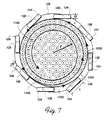
Fig. 7 shows a schematic, plan view from above of electron trajectories of the
deposition systems 100 in accordance with the embodiments of Figs. 1-5. As shown in
Fig. 7,
magnetic field lines 1100, generated by
electromagnet coils 1000 and 1010, as
in the embodiments of Figs. 1-5, cause the energized electrons in the high
density
electron cloud 900 to cycle in
spiral paths 1200 around the magnetic field lines 1100.
As shown in Fig. 7, the
electron guns 104 are arranged to inject the energetic electrons
substantially tangentially into the interior of
chamber shield 106. Also as shown in
Fig. 7, an electron at radial (vector) distance r from the center of high
density electron
cloud 900 has a (vector) velocity v directed tangentially along the
spiral path 1200. The
spiral paths 1200 shown in Fig. 7 are appropriate for electrons since the
magnetic field
lines 1100 are coming out of the plane of the figure in Fig. 7. The magnetic component
of the Lorentz force in the ith direction F
im on an electron moving with velocity v
j in the
jth direction in a magnetic field B
k in the kth direction (the directions 1, 2 and 3 forming
a right-handed coordinate system) is given by
where the absolute value of the electric charge e of an electron is
1.6021892±0.0000046×10
-19 Coulombs, the speed of light c is
2.99792458±0.000000012×10
10 cm/sec, ε
ijk is the completely antisymmetric tensor
(ε
123=1=ε
231=ε
312=-ε
213=-ε
132=-ε
321, all other components vanishing identically), the rest
mass of an electron m
e is 0.511 MeV/c
2, the magnitude of the electron's velocity is v,
the radius of the electron's orbit is r, and the unit vector in the ith direction is x
i/r, the
last equality following by equating the magnetic component of the Lorentz force on the
electron to the centripetal force on the electron. For example, in Fig. 7, with the 1
direction horizontal, the 2 direction vertical and the 3 direction normal to, and coming
out of, the plane of the figure, since the magnetic field lines 1100 are coming out of the
plane of the figure in the positive 3 direction (B
1=0, B
2=0, B
3=B), when the electron's
velocity in the plane of the figure is upward in the positive 2 direction (v
1=0, v
2=v, v
3=0),
the magnetic component of the Lorentz force is to the left in the negative 1 direction
(F
1m=-ε
123ev
2B
3/c=-evB/c, F
2m=0, F
3m=0); when the electron's velocity in the plane of the
figure is to the left in the negative 1 direction (v
1=-v, v
2=0, v
3=0), the magnetic
component of the Lorentz force is downward in the negative 2 direction (F
1m=0,
F
2m=-ε
213ev
1B
3/c=-evB/c, F
3m=0); when the electron's velocity in the plane of the figure
is downward in the negative 2 direction (v
1=0, v
2=-v, v
3=0), the magnetic component of
the Lorentz force is to the right in the positive 1 direction (F
1m=-ε
123ev
2B
3/c=evB/c,
F
2m=0, F
3m=0); and when the electron's velocity in the plane of the figure is to the right
in the positive 1 direction (v
1=v, v
2=0, v
3=0), the magnetic component of the Lorentz
force is upward in the positive 2 direction (F
1m=0, F
2m=-ε
213ev
1B
3/c=evB/c, F
3m=0),
resulting in a counterclockwise rotation of the electron in the plane of the figure, as
shown in Fig. 7.
For the counterclockwise rotation of the electron in the plane of the figure, as
shown in Fig. 7, equating the magnitudes in the above-given equation for the magnetic
component of the Lorentz force gives the radius r of the electron's orbit
r = c eB mev = c eB (2meE) 12
where the kinetic energy E of the electron is ½mev2 so that 2meE is (mev)2, the square of
the electron's (non-relativistic) momentum. As the kinetic energy E of the electron
decreases, for example, as the result of collisions with argon and titanium atoms in the
high density electron cloud 900, the radius r of the electron's orbit decreases as E½,
spiraling inward toward a central region of the high density electron cloud 900 within
the deposition system 100, as shown by the spiral path 1200 in Fig. 7. Electrons are
believed to create ions by colliding with gas and/or metal atoms with sufficient energy.
By magnetically trapping electrons, more ionizations are believed to occur.
The chamber shield 106 protects the vacuum chamber walls 108 from the
material being deposited. In the illustrated embodiment, the chamber shield 106 is
made of a conductive material such as heavy-duty, bead-blasted solid high-purity
(preferably 99.995% pure) titanium formed into a generally cylindrical shape having a
diameter of 25-36 cm (10-14 inches). However, other highly conductive materials may
be utilized depending upon the material being sputtered and other factors.
The material of the structure which will be coated should have a coefficient of
thermal expansion which closely matches that of the material being sputtered to reduce
flaking of sputtered material from the shield or other chamber internal structure onto the
wafer. In addition, the material to be coated should have good adhesion to the
sputtered material. Thus for example if the deposited material is titanium, the preferred
metal of the shields, brackets and other structures likely to be coated is bead-blasted
titanium. Any surfaces which are likely to sputter would preferably be made of the same
type of material as the target such as high purity titanium, for example. Of course, if the
material to be deposited is a material other than titanium, the preferred metal is the
deposited material, stainless steel or copper. Adherence can also be improved by
coating the structures with molybdenum prior to sputtering the target. However, it is
preferred that the coil (or any other surface likely to sputter) not be coated with
molybdenum or other materials since the molybdenum can contaminate the workpiece
if sputtered from the coil.
The chamber shield 106 is generally bowl-shaped (Fig. 2) and includes a
generally cylindrically shaped, vertically oriented wall 140. The chamber shield 106
further has a generally annular-shaped floor wall 142 which surrounds the pedestal 114
which supports the substrate 112 which has a 20 cm (8") diameter in the illustrated
embodiment. A clamp ring 154 may be used to clamp the substrate 112 to the pedestal
114 and cover the gap between the floor wall of the chamber shield 106 and the
pedestal 114.
The deposition system 100 is supported by an adapter ring assembly 152 which
engages an upper annular flange 150 of the vacuum chamber wall 108. The outer
shield 106 is grounded to the system ground through the adapter ring assembly 152.
The darkspace shield 130, like the chamber shield 106, is grounded through the
adapter ring assembly 152. The darkspace shield 130 also has an upper flange 170
which is fastened to the horizontal flange 162 of the adapter ring assembly 152. The
darkspace shield 130, like the chamber shield 106, is grounded through the adapter
ring assembly 152.
The target 110 is generally disk-shaped and is also supported by the adapter
ring assembly 152. However, the target 110 is negatively biased and therefore should
be insulated from the adapter ring assembly 152 which is grounded. Accordingly,
seated in a circular channel 176 formed in the underside of the target 110 is a ceramic
insulation ring assembly 172 which is also seated in a corresponding channel 174 in
the upper side of the adapter ring assembly 152. The insulator ring assembly 172
which may be made of a variety of insulative materials including ceramics spaces the
target 110 from the adapter ring assembly 152 so that the target 110 may be
adequately negatively biased. The target, adapter and ceramic ring assembly are
provided with O-ring sealing surfaces 178 to provide a vacuum tight assembly from the
vacuum chamber 102 to the target 110.
To promote uniform erosion of the target 110, a magnetron 116 (Fig. 2) may be
provided above the target 110. However, in some applications the magnetron might be
omitted by increasing the energetic electron injection ionization of the high density
electron cloud 900.
A DC power setting for biasing the target 110 of 3 kW is preferred but a range of
2-5 kW and a pedestal bias voltage of -30 volts DC is believed to be satisfactory for
many applications.
The substrate 112 to target 110 spacing is preferably about 140 mm but can
range from about 8 cm to 20 cm (3" to 8"). For this substrate 112 to target 110 spacing,
a chamber shield diameter of about 36 cm (14 inches) is preferred.
A variety of gases may be utilized in the plasma chamber 100, including Ar, H2 or
reactive gases such as NF3, CF4 and many others. Various gas pressures are suitable
including pressures of about 0.1 milliTorr or less. For ionized PVD, a pressure less
than or equal to about 5×10⁻⁴ Torr (0.5 milliTorr or 500 microTorr) is suitable for
ionization of sputtered material.
It will, of course, be understood that modifications of the present invention, in its
various aspects, will be apparent to those skilled in the art, some being apparent only
after study others being matters of routine mechanical and electronic design. Other
embodiments are also possible, their specific designs depending upon the particular
application. As such, the scope of the invention should not be limited by the particular
embodiments herein described but should be defined only by the appended claims and
equivalents thereof.