EP0864901A2 - Gasgedämpfter mikromechanischer Modulator - Google Patents
Gasgedämpfter mikromechanischer Modulator Download PDFInfo
- Publication number
- EP0864901A2 EP0864901A2 EP98301578A EP98301578A EP0864901A2 EP 0864901 A2 EP0864901 A2 EP 0864901A2 EP 98301578 A EP98301578 A EP 98301578A EP 98301578 A EP98301578 A EP 98301578A EP 0864901 A2 EP0864901 A2 EP 0864901A2
- Authority
- EP
- European Patent Office
- Prior art keywords
- gas
- layer
- movable member
- frequency
- modulator
- Prior art date
- Legal status (The legal status is an assumption and is not a legal conclusion. Google has not performed a legal analysis and makes no representation as to the accuracy of the status listed.)
- Granted
Links
- 239000007789 gas Substances 0.000 claims description 44
- 230000004044 response Effects 0.000 claims description 41
- 230000003287 optical effect Effects 0.000 claims description 23
- 239000001257 hydrogen Substances 0.000 claims description 6
- 229910052739 hydrogen Inorganic materials 0.000 claims description 6
- 230000033001 locomotion Effects 0.000 claims description 5
- UFHFLCQGNIYNRP-UHFFFAOYSA-N Hydrogen Chemical compound [H][H] UFHFLCQGNIYNRP-UHFFFAOYSA-N 0.000 claims description 4
- 229910052756 noble gas Inorganic materials 0.000 claims description 2
- 150000002835 noble gases Chemical class 0.000 claims 1
- 230000003534 oscillatory effect Effects 0.000 claims 1
- 238000013016 damping Methods 0.000 abstract description 30
- 239000012528 membrane Substances 0.000 description 45
- 230000014509 gene expression Effects 0.000 description 19
- 239000000758 substrate Substances 0.000 description 10
- SWQJXJOGLNCZEY-UHFFFAOYSA-N helium atom Chemical compound [He] SWQJXJOGLNCZEY-UHFFFAOYSA-N 0.000 description 9
- 241000208967 Polygala cruciata Species 0.000 description 8
- 239000001307 helium Substances 0.000 description 8
- 229910052734 helium Inorganic materials 0.000 description 8
- 238000000034 method Methods 0.000 description 6
- GKAOGPIIYCISHV-UHFFFAOYSA-N neon atom Chemical compound [Ne] GKAOGPIIYCISHV-UHFFFAOYSA-N 0.000 description 6
- 230000008859 change Effects 0.000 description 5
- 238000006073 displacement reaction Methods 0.000 description 5
- 229910052754 neon Inorganic materials 0.000 description 5
- XKRFYHLGVUSROY-UHFFFAOYSA-N Argon Chemical compound [Ar] XKRFYHLGVUSROY-UHFFFAOYSA-N 0.000 description 4
- 238000013461 design Methods 0.000 description 3
- 229910052581 Si3N4 Inorganic materials 0.000 description 2
- 229910052786 argon Inorganic materials 0.000 description 2
- 238000004891 communication Methods 0.000 description 2
- 230000007423 decrease Effects 0.000 description 2
- 230000003247 decreasing effect Effects 0.000 description 2
- 150000002431 hydrogen Chemical class 0.000 description 2
- -1 i.e. Chemical compound 0.000 description 2
- 229910052751 metal Inorganic materials 0.000 description 2
- 239000002184 metal Substances 0.000 description 2
- 238000002310 reflectometry Methods 0.000 description 2
- HQVNEWCFYHHQES-UHFFFAOYSA-N silicon nitride Chemical compound N12[Si]34N5[Si]62N3[Si]51N64 HQVNEWCFYHHQES-UHFFFAOYSA-N 0.000 description 2
- XUIMIQQOPSSXEZ-UHFFFAOYSA-N Silicon Chemical compound [Si] XUIMIQQOPSSXEZ-UHFFFAOYSA-N 0.000 description 1
- RTAQQCXQSZGOHL-UHFFFAOYSA-N Titanium Chemical compound [Ti] RTAQQCXQSZGOHL-UHFFFAOYSA-N 0.000 description 1
- 230000009471 action Effects 0.000 description 1
- 230000005540 biological transmission Effects 0.000 description 1
- 230000006835 compression Effects 0.000 description 1
- 238000007906 compression Methods 0.000 description 1
- 239000004020 conductor Substances 0.000 description 1
- 238000011161 development Methods 0.000 description 1
- 230000005611 electricity Effects 0.000 description 1
- 239000000835 fiber Substances 0.000 description 1
- PCHJSUWPFVWCPO-UHFFFAOYSA-N gold Chemical compound [Au] PCHJSUWPFVWCPO-UHFFFAOYSA-N 0.000 description 1
- 239000010931 gold Substances 0.000 description 1
- 229910052737 gold Inorganic materials 0.000 description 1
- 238000013507 mapping Methods 0.000 description 1
- 239000000463 material Substances 0.000 description 1
- 230000007246 mechanism Effects 0.000 description 1
- 230000009467 reduction Effects 0.000 description 1
- 230000000630 rising effect Effects 0.000 description 1
- 229910052710 silicon Inorganic materials 0.000 description 1
- 239000010703 silicon Substances 0.000 description 1
- 238000010408 sweeping Methods 0.000 description 1
- 239000010936 titanium Substances 0.000 description 1
- 229910052719 titanium Inorganic materials 0.000 description 1
Images







Classifications
-
- F—MECHANICAL ENGINEERING; LIGHTING; HEATING; WEAPONS; BLASTING
- F16—ENGINEERING ELEMENTS AND UNITS; GENERAL MEASURES FOR PRODUCING AND MAINTAINING EFFECTIVE FUNCTIONING OF MACHINES OR INSTALLATIONS; THERMAL INSULATION IN GENERAL
- F16F—SPRINGS; SHOCK-ABSORBERS; MEANS FOR DAMPING VIBRATION
- F16F9/00—Springs, vibration-dampers, shock-absorbers, or similarly-constructed movement-dampers using a fluid or the equivalent as damping medium
- F16F9/02—Springs, vibration-dampers, shock-absorbers, or similarly-constructed movement-dampers using a fluid or the equivalent as damping medium using gas only or vacuum
-
- G—PHYSICS
- G02—OPTICS
- G02B—OPTICAL ELEMENTS, SYSTEMS OR APPARATUS
- G02B26/00—Optical devices or arrangements for the control of light using movable or deformable optical elements
- G02B26/02—Optical devices or arrangements for the control of light using movable or deformable optical elements for controlling the intensity of light
Definitions
- the present invention relates generally to high speed micromechanical structures.
- a micromechanical optical modulator is useful for encoding data onto an optical signal for transmission through an optical communications network.
- a modulator has a variable gap defined by two layers of material, one of which layers is movable towards the other layer.
- the change in the location of the movable layer relative to the other layer, which is typically a nonmoving substrate layer, and the concominant change in the size of the gap, alters the optical properties of the modulator.
- Such a change in optical properties can be used to modulate an optical signal.
- optical modulators For some applications, such as Ether Net and high-definition television, optical modulators will be required to operate at 10 Megabits per second or more. Most conventional micromechanical modulators are typically limited, however, to data (bit) rates of about 2 Megabits per second.
- Improved squeeze-type micromechanical structures operate above atmospheric pressure. Further, in accordance with the present invention, such structures have a minimum porosity, 1/ ( ⁇ o ⁇ ), of about 1.4 and a minimum reduced pressure or gas frequency, ⁇ g / ⁇ o , of about 1.25.
- High-speed operation of such devices at less than about 10 percent "ringing" requires that ⁇ g / ⁇ o > 1.25 and 0.25 + 0.7( ⁇ g / ⁇ o ) 2 - 0.8( ⁇ g / ⁇ o - 1.25) ⁇ 1/ ( ⁇ o ⁇ ) ⁇ 0.25 + 0.7( ⁇ g / ⁇ o ) 2 + ( ⁇ g / ⁇ o - 1.25).
- the present invention is applicable to "squeeze-type" micromechanical structures wherein a volume of gas is compressed as a movable layer or member of such a structure moves.
- squeeze-type micromechanical structure is a drum-head micromechanical modulator possessing damping holes as described in U.S. Patent Application S.N. 08/565,453.
- Illustrative embodiments presented herein are directed to such drum-head micromechanical optical modulators. It should be understood, however, that the present invention applies to other squeeze-type structures as well.
- Application number 08/565,453 is incorporated by reference herein.
- FIGS. 1 and 2 An exemplary drum-head micromechanical modulator having damping holes is illustrated in FIGS. 1 and 2.
- the modulator has a movable layer or member or "membrane" 15 that is suspended, via a layer 12, over a nonmoving layer or substrate 10, defining a gap 20 therebetween.
- the membrane 15 forms a continous surface that overlaps, at every point, the perimeter 19 of modulator cavity 21 defined in the layer 12.
- a plurality of holes 14 are arranged in a preferably regular pattern across the membrane 15.
- the holes 14 are located beginning outside of a centrally located region 16 that forms an "optical window."
- the optical window 16 is typically in optical communication with an optical waveguide or fiber, not shown, that delivers an optical signal 2 to the modulator.
- holes 14 can be located within the optical window 16, although their presence in that region of the membrane 15 may affect the optical properties of the modulator.
- the modulator, or, more generally, other squeeze-type micromechanical structures can be configured so that the damping holes 14 are located in another part of the structure, such as in the layer 12, and allow gas to move out of the region beneath the membrane or movable member 15, i.e., the modulator cavity, to provide damping.
- the modulator is enclosed within a hermetic seal 33 using known techniques.
- the hermetically sealed modulator is under a gas atmosphere, preferably hydrogen or a noble gas, i.e., helium, neon, and the like. Pressure in the region 35 above the membrane is referred to as the ambient pressure of the modulator or the membrane.
- the membrane 15 must be conductive, or, in other embodiments such as shown in FIGS. 1 and 2, have a layer 30 of conductive material disposed thereon.
- the membrane 15 and substrate 10 are placed in electrical contact with controlled voltage source 29.
- a contact 31 may be deposited on the substrate 10 to facilitate wire bonding to the controlled voltage source.
- the membrane 15 moves between a quiescent or equilibrium position towards the substrate under the action of the controlled voltage source 29. Movement of the membrane 15 changes the size of the gap 20, which changes the reflectivity of the modulator.
- FIG. 3 is a plot of 1/ ( ⁇ o ⁇ ) versus ⁇ g / ⁇ o .
- the parameter 1/ ⁇ is a measure of the membrane's porosity. See Section II. 1.
- the parameter ⁇ g referred to as the gas frequency, is a measure of the contribution to the resonant frequency of the membrane that is associated with the compression of the gas.
- ⁇ g is proportional to the square root of the ambient pressure, P o , and can thus be used as a measure of pressure.
- the parameter ⁇ o is the natural (vacuum) resonant frequency of the membrane. See Sections II.1, II.2.
- the parameter ⁇ o is used to express the membrane parameters in reduced (dimensionless) quantities.
- region 40 defines an operating regime in which membrane ringing will be limited to 10 percent or less.
- the region 40 is defined herein as an "acceptable" operating regime for at least some uses of a modulator. More particularly, region 42 defines an operating regime having 5 to 10 percent ringing, and region 44 defines an operating regime having from 0 to 5 percent ringing.
- FIG. 3 indicates that threshold values of 1/ ( ⁇ o ⁇ ) and ⁇ g / ⁇ o must be met to achieve acceptable operation. Specifically, the parameter 1/ ( ⁇ o ⁇ ) must be greater than about 1.4 and the parameter ⁇ g / ⁇ o must be greater than about 1.3.
- the reduced gas frequency of a drum head modulator should be at least 1.3, and 0.25 + 0.7( ⁇ g / ⁇ o ) 2 - 0.8( ⁇ g / ⁇ o - 1.25) ⁇ 1/ ( ⁇ o ⁇ ) ⁇ 0.25 + 0.7( ⁇ g / ⁇ o ) 2 + ( ⁇ g / ⁇ o - 1.25).
- Section II Methods and expressions for determining the value of 1/ ⁇ and ⁇ g are presented in Section II.
- the methodology described in Section II.9 is used to provide a "first guess" at the device design, i.e., number of damping holes, etc.
- a device is then built according to the first guess, and values of 1/ ⁇ and ⁇ g are extracted from measured frequency response curves for the device, as described in Section II.8A.
- a scaling factor can then be applied to achieve satisfactory square-wave response, i.e., adjust the device's operation to fall within the desired region of FIG. 3.
- Such a scaling factor can be determined by applying an appropriate multiplier to the plot of 1/( ⁇ o ⁇ ) versus ⁇ g / ⁇ o obtained for the "first guess" device to bring it within a region of acceptable performance, as defined in FIG. 3.
- bit rate 0.65x3 ⁇ 2 Megabits per sec.
- Section II of this specification the underlying theory and model development for the invention described in Section I is presented.
- the model incorporates the essential elements of an actual gas-damped device for which the mechanical response can be determined analytically.
- the model device shown in Fig. 4 consists of a piston of mass, m, and cross-sectional area, a, that is supported within a cylinder by a mechanical spring having spring constant k.
- the piston has small holes that provide an escape for gas trapped in the cylinder.
- the piston sits a distance, h, above the bottom of the cylinder. Because the assembly is located in a large volume, the gas pressure above the piston remains at the ambient gas pressure, P o , independent of the piston's position and the instantaneous pressure, P, in the cylinder.
- x the piston's displacement from equilibrium and ⁇ is the ordinary damping constant associated with the piston's velocity.
- ⁇ will be a very complicated function depending on many parameters, including the number, size, and physical arrangement of the holes in the piston; the gap size h; the type of gas used and the mean free path of the gas molecules.
- ⁇ o 2 k/m
- g 2 ( a P o /h) / m.
- the characteristic frequency f o ⁇ o / 2 ⁇ of a micromechanical structure lies in the broad frequency range between low kHz and low MHz.
- FIG. 5 shows f g plotted as a function of pressure at a gap of ⁇ /4 (reference numeral 50) and a gap of 3 ⁇ /4 (reference numeral 52).
- ⁇ o / ⁇ g 2.
- the frequency response exhibits a more "regular" pattern, with the reduced amplitude increasing monotonically from unity on the low frequency side of the peak.
- critical damping can be achieved by adjusting the piston's porosity. Critical damping is achieved in only those embodiments wherein ⁇ g / ⁇ o is sufficiently large.
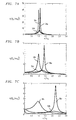
- displacement amplitude A is plotted versus ⁇ / ⁇ o for three values of 1/( ⁇ o ⁇ ) and a fixed value of ⁇ g / ⁇ o .
- ⁇ g / ⁇ o 2.
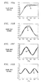
- High-speed switching applications require devices whose response to a discontinuous step change in drive exhibits a short rise time and no significant ringing.
- the response to a square-wave drive may be determined by simply summing the complex frequency responses to the Fourier components of the drive signal.
- FIGS. 9a, 9c, and 9e show frequency response curves
- frequency response curve 64 exhibits a significant drop in amplitude at low frequencies.
- Square-wave response curve 66 exhibits behavior characterized by two different time scales. In particular, the first time scale is determined by ⁇ , and the second is determined by f peak ⁇ (f o 2 + f g 2 ) 0.5 ⁇ (5) 0.5 .
- both the frequency response curve 72 and the square-wave response curve 74 exhibit behavior similar to that of an underdamped oscillator. Because f peak, at that limit, is close to the natural frequency f o , the ringing occurs at a much lower frequency than in the low porosity regime.
- the square-wave response 70 has a rise time characterized by f o and does not exhibit ringing.
- the frequency response curve 68 is substantially free of a resonance peak.
- FIG. 3 is a plot of 1/ ( ⁇ o ⁇ ) versus ⁇ g / ⁇ o, previously described in Section I of this specification.
- the plot indicates that a minimum pressure must be exceeded to achieve a clean square wave response, i.e., very low ringing, independent of piston (membrane) porosity. The existence of such a minimum pressure was previously unknown. Its discovery advantageously results in the ability to design "squeeze-type" micro-mechanical structures, such as modulators, with improved performance, especially when such device are operating at speeds well in excess of a few Mbits/s.
- Performance data were obtained on eight micro-mechanical optical modulators. Each modulator had a "drum-head" configuration as described in Section I, and included a stressed membrane comprised of silicon nitride. Metal comprising 100 angstroms of titanium and 500 angstroms of gold was disposed on the membrane of each modulator in an annular region around an optical window. The metal functioned as an electrode. Damping holes were placed through the electrode and the membrane.
- Each modulator also included a silicon substrate having a doped region suitable for conducting electricity. As a voltage was applied across the electrode and substrate, an electrostatic force was generated that caused the membrane to moves toward the substrate. The resulting membrane motion was detected by measuring the modulation in the reflectivity of the central, unmetallized portion of the membrane.
- FIGS. 11a - 11 d which show a top view of the "drum-head" membrane, illustrate four different embodiments of damping-hole layouts that were used for the eight modulators. Each of such layouts was used at two different gap spacings. One gap spacing was 0.39 microns ( ⁇ /4) and the other was 0.97 microns (0.62 ⁇ ).
- the dashed circle 84 indicates the perimeter of the membrane, i.e., the perimeter of the modulator cavity.
- the membranes had a diameter of 150 microns.
- the membrane had a diameter of 120 microns.
- the annular region 86 indicates the metallized region of the membrane.
- the small circles 88 within the region 86 are damping holes.
- the damping holes 88 in the layout shown in FIG. 1 1c have a diameter of 3 microns; the damping holes in FIGS. 11a, 11b and 11d have a diameter of 5 microns.
- the damping holes 88 are arranged in circular groupings. With reference to FIG. 11 a, the innermost circular grouping 90 of damping holes has a diameter of 40 microns, the outermost circular grouping 94 of damping holes has a diameter of 100 microns and the middle circular grouping 92 has a diameter of 70 microns.
- the optical window 96 is shown within the innermost circular grouping 90 of damping holes.
- dimensionless quantities can be related to the two parameters of the model, i.e., ⁇ g and 1/ ⁇ o ⁇ .
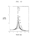
- FIGS. 12 and 13 the measured frequency response for Samples 2 and 5, under a helium atmosphere, are shown in FIGS. 12 and 13, respectively.
- the various curves in each Figure correspond to different helium pressures ranging from 0.2 to 3.0 bar, wherein those values are used to identify each curve in those Figures.
- Each curve has been normalized so that at zero frequency, the amplitude is unity.
- Such frequency response curves can be repeated for other gases, e.g., hydrogen, neon and the like, and for the other Sample modulators.
- the frequency and amplitude of measured resonance peaks extracted from such frequency response curves can then be plotted versus pressure.
- Corresponding values of ⁇ g / ⁇ o and 1/ ⁇ o ⁇ are then extracted using expression (8).
- FIG. 14 shows ⁇ g / ⁇ o plotted versus P 1/2 for Samples 2 (plot 98) and 5 (plot 100). The plot incorporates data obtained under hydrogen and neon atmospheres, as well as helium.
- FIG. 14 indicates that (i) ⁇ g / ⁇ o is proportional to P 1/2 , (ii) ⁇ g / ⁇ o is independent of gas type, and (iii) ⁇ g / ⁇ o varies inversely with gap spacing. Such observations are consistent with expressions (7) and (12).
- FIG. 15 shows plots of (1/ ⁇ o ⁇ ) 2 versus P 2 for hydrogen (102), helium (104) and neon (106) atmospheres.
- the intercepts and slopes of the lines 102, 104 and 106 determine ( ⁇ / ⁇ o ) 2 and ( ⁇ / ⁇ o ) 2 for each corresponding gas.
- both a and ⁇ are functions of the various physical dimensions of the device, e.g., modulator.
- 1/ ⁇ should be inversely proportional to the area of the device; in the case of the Sample modulators, that area is the membrane diameter D 2 .
- N is the number of damping holes of diameter d, assumed to be distributed "uniformly" over the membrane
- D is the device (membrane) diameter
- h is the gap between the movable layer (membrane) and the nonmoving layer (substrate) when the modulator is in the quiescent state
- ⁇ is the gas viscosity in units of 10 -5 poise
- M is the molecular weight of the gas
- P is the pressure in bar.
- the following example illustrates an application of the present invention, wherein the data rate and physical configuration of a modulator operating (satisfactorily) at substantially the fastest rate possible for a given set of conditions are determined.
- the example assumes a gap of 0.97 microns, a membrane diameter of 150 microns and a maximum argon pressure of 2 bar.
- f g 1.3P 1/2 for a modulator configured similarly to the modulator of the present example.
- f g 1.87 MHz.
- f o 0.93 MHz, corresponding to a maximum data rate of about 3 Mbits/sec.
- f o ⁇ 1/D [ S/ ⁇ ] 1/2 The natural frequency (with membrane diameter D fixed) can therefore be decreased by a factor of two by decreasing the membrane stress S, by a factor of four.
- the sample modulator had a stress of about 800 MPa, so the stress would have to be reduced to approximately 200 Mpa for the aforementioned reduction.
- average membrane density could be increased, such as by increasing the thickness of the electrode disposed on the membrane.
- membrane diameter D was fixed at 150 microns and the stress S was altered to change the natural frequency.
Landscapes
- Engineering & Computer Science (AREA)
- General Engineering & Computer Science (AREA)
- Physics & Mathematics (AREA)
- Mechanical Engineering (AREA)
- General Physics & Mathematics (AREA)
- Optics & Photonics (AREA)
- Mechanical Light Control Or Optical Switches (AREA)
- Micromachines (AREA)
Applications Claiming Priority (2)
| Application Number | Priority Date | Filing Date | Title |
|---|---|---|---|
| US08/815,774 US5786927A (en) | 1997-03-12 | 1997-03-12 | Gas-damped micromechanical structure |
| US815774 | 1997-03-12 |
Publications (3)
| Publication Number | Publication Date |
|---|---|
| EP0864901A2 true EP0864901A2 (de) | 1998-09-16 |
| EP0864901A3 EP0864901A3 (de) | 1998-10-21 |
| EP0864901B1 EP0864901B1 (de) | 2003-11-19 |
Family
ID=25218787
Family Applications (1)
| Application Number | Title | Priority Date | Filing Date |
|---|---|---|---|
| EP98301578A Expired - Lifetime EP0864901B1 (de) | 1997-03-12 | 1998-03-03 | Gasgedämpfter mikromechanischer Modulator |
Country Status (4)
| Country | Link |
|---|---|
| US (1) | US5786927A (de) |
| EP (1) | EP0864901B1 (de) |
| JP (1) | JP3212552B2 (de) |
| DE (1) | DE69819797T2 (de) |
Families Citing this family (101)
| Publication number | Priority date | Publication date | Assignee | Title |
|---|---|---|---|---|
| US7808694B2 (en) * | 1994-05-05 | 2010-10-05 | Qualcomm Mems Technologies, Inc. | Method and device for modulating light |
| US7123216B1 (en) | 1994-05-05 | 2006-10-17 | Idc, Llc | Photonic MEMS and structures |
| US7852545B2 (en) | 1994-05-05 | 2010-12-14 | Qualcomm Mems Technologies, Inc. | Method and device for modulating light |
| US7460291B2 (en) * | 1994-05-05 | 2008-12-02 | Idc, Llc | Separable modulator |
| WO1999052006A2 (en) * | 1998-04-08 | 1999-10-14 | Etalon, Inc. | Interferometric modulation of radiation |
| US7532377B2 (en) | 1998-04-08 | 2009-05-12 | Idc, Llc | Movable micro-electromechanical device |
| US8928967B2 (en) | 1998-04-08 | 2015-01-06 | Qualcomm Mems Technologies, Inc. | Method and device for modulating light |
| WO2003007049A1 (en) | 1999-10-05 | 2003-01-23 | Iridigm Display Corporation | Photonic mems and structures |
| JP2002023070A (ja) * | 2000-07-04 | 2002-01-23 | Sony Corp | 光学多層構造体および光スイッチング素子、並びに画像表示装置 |
| DE10117170A1 (de) * | 2001-04-06 | 2002-10-10 | Zeiss Carl Jena Gmbh | Anordnung zum Druckausgleich für optische Geräte |
| US20030082606A1 (en) * | 2001-09-04 | 2003-05-01 | Lebo Roger V. | Optimizing genome-wide mutation analysis of chromosomes and genes |
| JP4736282B2 (ja) * | 2001-09-05 | 2011-07-27 | ソニー株式会社 | 薄膜光学装置 |
| US6794119B2 (en) | 2002-02-12 | 2004-09-21 | Iridigm Display Corporation | Method for fabricating a structure for a microelectromechanical systems (MEMS) device |
| US6574033B1 (en) | 2002-02-27 | 2003-06-03 | Iridigm Display Corporation | Microelectromechanical systems device and method for fabricating same |
| TW200413810A (en) | 2003-01-29 | 2004-08-01 | Prime View Int Co Ltd | Light interference display panel and its manufacturing method |
| US7476327B2 (en) * | 2004-05-04 | 2009-01-13 | Idc, Llc | Method of manufacture for microelectromechanical devices |
| WO2006014929A1 (en) | 2004-07-29 | 2006-02-09 | Idc, Llc | System and method for micro-electromechanical operating of an interferometric modulator |
| US7944599B2 (en) | 2004-09-27 | 2011-05-17 | Qualcomm Mems Technologies, Inc. | Electromechanical device with optical function separated from mechanical and electrical function |
| US7304784B2 (en) | 2004-09-27 | 2007-12-04 | Idc, Llc | Reflective display device having viewable display on both sides |
| US7289259B2 (en) | 2004-09-27 | 2007-10-30 | Idc, Llc | Conductive bus structure for interferometric modulator array |
| US7302157B2 (en) | 2004-09-27 | 2007-11-27 | Idc, Llc | System and method for multi-level brightness in interferometric modulation |
| US7130104B2 (en) * | 2004-09-27 | 2006-10-31 | Idc, Llc | Methods and devices for inhibiting tilting of a mirror in an interferometric modulator |
| US7420725B2 (en) | 2004-09-27 | 2008-09-02 | Idc, Llc | Device having a conductive light absorbing mask and method for fabricating same |
| US7684104B2 (en) | 2004-09-27 | 2010-03-23 | Idc, Llc | MEMS using filler material and method |
| US7630119B2 (en) | 2004-09-27 | 2009-12-08 | Qualcomm Mems Technologies, Inc. | Apparatus and method for reducing slippage between structures in an interferometric modulator |
| US7936497B2 (en) | 2004-09-27 | 2011-05-03 | Qualcomm Mems Technologies, Inc. | MEMS device having deformable membrane characterized by mechanical persistence |
| US7564612B2 (en) | 2004-09-27 | 2009-07-21 | Idc, Llc | Photonic MEMS and structures |
| US7893919B2 (en) * | 2004-09-27 | 2011-02-22 | Qualcomm Mems Technologies, Inc. | Display region architectures |
| US7527995B2 (en) | 2004-09-27 | 2009-05-05 | Qualcomm Mems Technologies, Inc. | Method of making prestructure for MEMS systems |
| US8008736B2 (en) | 2004-09-27 | 2011-08-30 | Qualcomm Mems Technologies, Inc. | Analog interferometric modulator device |
| US7612932B2 (en) * | 2004-09-27 | 2009-11-03 | Idc, Llc | Microelectromechanical device with optical function separated from mechanical and electrical function |
| US7583429B2 (en) | 2004-09-27 | 2009-09-01 | Idc, Llc | Ornamental display device |
| US7369296B2 (en) | 2004-09-27 | 2008-05-06 | Idc, Llc | Device and method for modifying actuation voltage thresholds of a deformable membrane in an interferometric modulator |
| US7554714B2 (en) | 2004-09-27 | 2009-06-30 | Idc, Llc | Device and method for manipulation of thermal response in a modulator |
| US7327510B2 (en) * | 2004-09-27 | 2008-02-05 | Idc, Llc | Process for modifying offset voltage characteristics of an interferometric modulator |
| US7321456B2 (en) | 2004-09-27 | 2008-01-22 | Idc, Llc | Method and device for corner interferometric modulation |
| US7719500B2 (en) | 2004-09-27 | 2010-05-18 | Qualcomm Mems Technologies, Inc. | Reflective display pixels arranged in non-rectangular arrays |
| US7372613B2 (en) | 2004-09-27 | 2008-05-13 | Idc, Llc | Method and device for multistate interferometric light modulation |
| US7884989B2 (en) | 2005-05-27 | 2011-02-08 | Qualcomm Mems Technologies, Inc. | White interferometric modulators and methods for forming the same |
| US7630114B2 (en) * | 2005-10-28 | 2009-12-08 | Idc, Llc | Diffusion barrier layer for MEMS devices |
| US7916980B2 (en) | 2006-01-13 | 2011-03-29 | Qualcomm Mems Technologies, Inc. | Interconnect structure for MEMS device |
| US7550810B2 (en) | 2006-02-23 | 2009-06-23 | Qualcomm Mems Technologies, Inc. | MEMS device having a layer movable at asymmetric rates |
| US7649671B2 (en) | 2006-06-01 | 2010-01-19 | Qualcomm Mems Technologies, Inc. | Analog interferometric modulator device with electrostatic actuation and release |
| US7471442B2 (en) * | 2006-06-15 | 2008-12-30 | Qualcomm Mems Technologies, Inc. | Method and apparatus for low range bit depth enhancements for MEMS display architectures |
| US7835061B2 (en) | 2006-06-28 | 2010-11-16 | Qualcomm Mems Technologies, Inc. | Support structures for free-standing electromechanical devices |
| US7385744B2 (en) | 2006-06-28 | 2008-06-10 | Qualcomm Mems Technologies, Inc. | Support structure for free-standing MEMS device and methods for forming the same |
| US7527998B2 (en) | 2006-06-30 | 2009-05-05 | Qualcomm Mems Technologies, Inc. | Method of manufacturing MEMS devices providing air gap control |
| US7629197B2 (en) | 2006-10-18 | 2009-12-08 | Qualcomm Mems Technologies, Inc. | Spatial light modulator |
| US7545552B2 (en) | 2006-10-19 | 2009-06-09 | Qualcomm Mems Technologies, Inc. | Sacrificial spacer process and resultant structure for MEMS support structure |
| US20080111834A1 (en) * | 2006-11-09 | 2008-05-15 | Mignard Marc M | Two primary color display |
| US8115987B2 (en) | 2007-02-01 | 2012-02-14 | Qualcomm Mems Technologies, Inc. | Modulating the intensity of light from an interferometric reflector |
| CA2578319A1 (en) * | 2007-02-12 | 2008-08-12 | Steve Larter | Method and apparatus for obtaining heavy oil samples from a reservoir sample |
| US7742220B2 (en) | 2007-03-28 | 2010-06-22 | Qualcomm Mems Technologies, Inc. | Microelectromechanical device and method utilizing conducting layers separated by stops |
| US7643202B2 (en) | 2007-05-09 | 2010-01-05 | Qualcomm Mems Technologies, Inc. | Microelectromechanical system having a dielectric movable membrane and a mirror |
| US7715085B2 (en) * | 2007-05-09 | 2010-05-11 | Qualcomm Mems Technologies, Inc. | Electromechanical system having a dielectric movable membrane and a mirror |
| US7719752B2 (en) | 2007-05-11 | 2010-05-18 | Qualcomm Mems Technologies, Inc. | MEMS structures, methods of fabricating MEMS components on separate substrates and assembly of same |
| US8111262B2 (en) * | 2007-05-18 | 2012-02-07 | Qualcomm Mems Technologies, Inc. | Interferometric modulator displays with reduced color sensitivity |
| US7643199B2 (en) * | 2007-06-19 | 2010-01-05 | Qualcomm Mems Technologies, Inc. | High aperture-ratio top-reflective AM-iMod displays |
| US7782517B2 (en) | 2007-06-21 | 2010-08-24 | Qualcomm Mems Technologies, Inc. | Infrared and dual mode displays |
| US7630121B2 (en) | 2007-07-02 | 2009-12-08 | Qualcomm Mems Technologies, Inc. | Electromechanical device with optical function separated from mechanical and electrical function |
| US7813029B2 (en) | 2007-07-31 | 2010-10-12 | Qualcomm Mems Technologies, Inc. | Devices and methods for enhancing color shift of interferometric modulators |
| US8072402B2 (en) | 2007-08-29 | 2011-12-06 | Qualcomm Mems Technologies, Inc. | Interferometric optical modulator with broadband reflection characteristics |
| US7847999B2 (en) | 2007-09-14 | 2010-12-07 | Qualcomm Mems Technologies, Inc. | Interferometric modulator display devices |
| US7773286B2 (en) | 2007-09-14 | 2010-08-10 | Qualcomm Mems Technologies, Inc. | Periodic dimple array |
| KR20100090257A (ko) | 2007-10-19 | 2010-08-13 | 퀄컴 엠이엠스 테크놀로지스, 인크. | 광기전력 소자가 통합된 디스플레이 |
| US8058549B2 (en) | 2007-10-19 | 2011-11-15 | Qualcomm Mems Technologies, Inc. | Photovoltaic devices with integrated color interferometric film stacks |
| CN101836137A (zh) | 2007-10-23 | 2010-09-15 | 高通Mems科技公司 | 基于微机电系统的可调整透射装置 |
| US8941631B2 (en) | 2007-11-16 | 2015-01-27 | Qualcomm Mems Technologies, Inc. | Simultaneous light collection and illumination on an active display |
| US7715079B2 (en) | 2007-12-07 | 2010-05-11 | Qualcomm Mems Technologies, Inc. | MEMS devices requiring no mechanical support |
| US8164821B2 (en) | 2008-02-22 | 2012-04-24 | Qualcomm Mems Technologies, Inc. | Microelectromechanical device with thermal expansion balancing layer or stiffening layer |
| US7944604B2 (en) | 2008-03-07 | 2011-05-17 | Qualcomm Mems Technologies, Inc. | Interferometric modulator in transmission mode |
| US7612933B2 (en) | 2008-03-27 | 2009-11-03 | Qualcomm Mems Technologies, Inc. | Microelectromechanical device with spacing layer |
| US7898723B2 (en) | 2008-04-02 | 2011-03-01 | Qualcomm Mems Technologies, Inc. | Microelectromechanical systems display element with photovoltaic structure |
| US7969638B2 (en) | 2008-04-10 | 2011-06-28 | Qualcomm Mems Technologies, Inc. | Device having thin black mask and method of fabricating the same |
| US7746539B2 (en) | 2008-06-25 | 2010-06-29 | Qualcomm Mems Technologies, Inc. | Method for packing a display device and the device obtained thereof |
| US8023167B2 (en) | 2008-06-25 | 2011-09-20 | Qualcomm Mems Technologies, Inc. | Backlight displays |
| US7768690B2 (en) | 2008-06-25 | 2010-08-03 | Qualcomm Mems Technologies, Inc. | Backlight displays |
| US7859740B2 (en) | 2008-07-11 | 2010-12-28 | Qualcomm Mems Technologies, Inc. | Stiction mitigation with integrated mech micro-cantilevers through vertical stress gradient control |
| US7855826B2 (en) | 2008-08-12 | 2010-12-21 | Qualcomm Mems Technologies, Inc. | Method and apparatus to reduce or eliminate stiction and image retention in interferometric modulator devices |
| US8358266B2 (en) | 2008-09-02 | 2013-01-22 | Qualcomm Mems Technologies, Inc. | Light turning device with prismatic light turning features |
| US8270056B2 (en) | 2009-03-23 | 2012-09-18 | Qualcomm Mems Technologies, Inc. | Display device with openings between sub-pixels and method of making same |
| WO2010138761A1 (en) | 2009-05-29 | 2010-12-02 | Qualcomm Mems Technologies, Inc. | Illumination devices and methods of fabrication thereof |
| US8270062B2 (en) | 2009-09-17 | 2012-09-18 | Qualcomm Mems Technologies, Inc. | Display device with at least one movable stop element |
| US8488228B2 (en) | 2009-09-28 | 2013-07-16 | Qualcomm Mems Technologies, Inc. | Interferometric display with interferometric reflector |
| KR20130100232A (ko) | 2010-04-09 | 2013-09-10 | 퀄컴 엠이엠에스 테크놀로지스, 인크. | 전기 기계 디바이스의 기계층 및 그 형성 방법 |
| CN103109315A (zh) | 2010-08-17 | 2013-05-15 | 高通Mems科技公司 | 对干涉式显示装置中的电荷中性电极的激活和校准 |
| US9057872B2 (en) | 2010-08-31 | 2015-06-16 | Qualcomm Mems Technologies, Inc. | Dielectric enhanced mirror for IMOD display |
| JP5914972B2 (ja) * | 2011-03-08 | 2016-05-11 | セイコーエプソン株式会社 | 光モジュールおよび光分析装置 |
| US8963159B2 (en) | 2011-04-04 | 2015-02-24 | Qualcomm Mems Technologies, Inc. | Pixel via and methods of forming the same |
| US9134527B2 (en) | 2011-04-04 | 2015-09-15 | Qualcomm Mems Technologies, Inc. | Pixel via and methods of forming the same |
| US8659816B2 (en) | 2011-04-25 | 2014-02-25 | Qualcomm Mems Technologies, Inc. | Mechanical layer and methods of making the same |
| US8736939B2 (en) | 2011-11-04 | 2014-05-27 | Qualcomm Mems Technologies, Inc. | Matching layer thin-films for an electromechanical systems reflective display device |
| US11119116B2 (en) | 2019-04-01 | 2021-09-14 | Honeywell International Inc. | Accelerometer for determining an acceleration based on modulated optical signals |
| US11079227B2 (en) | 2019-04-01 | 2021-08-03 | Honeywell International Inc. | Accelerometer system enclosing gas |
| US10705112B1 (en) | 2019-04-22 | 2020-07-07 | Honeywell International Inc. | Noise rejection for optomechanical devices |
| US10956768B2 (en) | 2019-04-22 | 2021-03-23 | Honeywell International Inc. | Feedback cooling and detection for optomechanical devices |
| US11408911B2 (en) | 2019-07-17 | 2022-08-09 | Honeywell International Inc. | Optomechanical structure with corrugated edge |
| US11119114B2 (en) | 2019-07-17 | 2021-09-14 | Honeywell International Inc. | Anchor structure for securing optomechanical structure |
| US11408912B2 (en) | 2019-08-13 | 2022-08-09 | Honeywell International Inc. | Feedthrough rejection for optomechanical devices |
| US11150264B2 (en) | 2019-08-13 | 2021-10-19 | Honeywell International Inc. | Feedthrough rejection for optomechanical devices using elements |
| US11372019B2 (en) | 2019-08-13 | 2022-06-28 | Honeywell International Inc. | Optomechanical resonator stabilization for optomechanical devices |
Family Cites Families (3)
| Publication number | Priority date | Publication date | Assignee | Title |
|---|---|---|---|---|
| DE69027163T2 (de) * | 1989-09-15 | 1996-11-14 | Texas Instruments Inc | Spatiallichtmodulator und Verfahren |
| US5280173A (en) * | 1992-01-31 | 1994-01-18 | Brown University Research Foundation | Electric and electromagnetic field sensing system including an optical transducer |
| DE4211898A1 (de) * | 1992-04-09 | 1993-10-28 | Deutsche Aerospace | Mikromechanischer Spiegel |
-
1997
- 1997-03-12 US US08/815,774 patent/US5786927A/en not_active Expired - Lifetime
-
1998
- 1998-02-23 JP JP04065698A patent/JP3212552B2/ja not_active Expired - Lifetime
- 1998-03-03 EP EP98301578A patent/EP0864901B1/de not_active Expired - Lifetime
- 1998-03-03 DE DE69819797T patent/DE69819797T2/de not_active Expired - Lifetime
Also Published As
| Publication number | Publication date |
|---|---|
| US5786927A (en) | 1998-07-28 |
| EP0864901B1 (de) | 2003-11-19 |
| DE69819797D1 (de) | 2003-12-24 |
| DE69819797T2 (de) | 2004-09-30 |
| EP0864901A3 (de) | 1998-10-21 |
| JP3212552B2 (ja) | 2001-09-25 |
| JPH10253900A (ja) | 1998-09-25 |
Similar Documents
| Publication | Publication Date | Title |
|---|---|---|
| EP0864901B1 (de) | Gasgedämpfter mikromechanischer Modulator | |
| Zalalutdinov et al. | Optically pumped parametric amplification for micromechanical oscillators | |
| US6400738B1 (en) | Tunable Fabry-Perot filters and lasers | |
| EP0788004B1 (de) | Struktur zur Membrandämpfung in einem mikromechanischen optischen Modulator | |
| EP1260019B1 (de) | Mikro-elektromechanische resonatorstruktur und herstellungsverfahren dafür | |
| US5528939A (en) | Micromechanical pressure gauge having extended sensor range | |
| US5831262A (en) | Article comprising an optical fiber attached to a micromechanical device | |
| US6787969B2 (en) | Damped micromechanical device | |
| US6356689B1 (en) | Article comprising an optical cavity | |
| WO2022223041A1 (zh) | 一种传感装置 | |
| JP2000511282A (ja) | 加速度計のための静電駆動装置 | |
| Lee et al. | A vacuum packaged differential resonant accelerometer using gap sensitive electrostatic stiffness changing effect | |
| JP3408945B2 (ja) | マルチ電極形マイクロ機械的構成の光変調器のための方法と装置 | |
| US8633787B2 (en) | Coupled MEMS structure for motion amplification | |
| US6724785B1 (en) | Tunable fabry-perot filters and lasers with reduced frequency noise | |
| JP4513366B2 (ja) | 機械共振器、フィルタおよび電気回路 | |
| Greywall et al. | Coupled micromechanical drumhead resonators with practical application as electromechanical bandpass filters | |
| CN115025959A (zh) | 一种中心支撑的压电式微机械超声换能器 | |
| Wu et al. | A high-performance bulk mode single crystal silicon microresonator based on a cavity-SOI wafer | |
| Robichaud et al. | Electromechanical tuning of piecewise stiffness and damping for long-range and high-precision piezoelectric ultrasonic transducers | |
| Howe | Microsensor and microactuator applications of thin films | |
| CN222170006U (zh) | 一种mems压电发声单元及mems压电扬声器 | |
| Daneshnazar et al. | Reaching High Velocities in Micromachined Resonant Structures via Electrostatic Metamaterial Actuation | |
| CN209030172U (zh) | 一种基于soi结构的薄膜声波滤波器 | |
| Ataro et al. | Tailored scaling: a possibility to improve the performance of ultra-wide continuously tunable photonic devices |
Legal Events
| Date | Code | Title | Description |
|---|---|---|---|
| PUAI | Public reference made under article 153(3) epc to a published international application that has entered the european phase |
Free format text: ORIGINAL CODE: 0009012 |
|
| PUAL | Search report despatched |
Free format text: ORIGINAL CODE: 0009013 |
|
| AK | Designated contracting states |
Kind code of ref document: A2 Designated state(s): DE FR GB |
|
| AX | Request for extension of the european patent |
Free format text: AL;LT;LV;MK;RO;SI |
|
| AK | Designated contracting states |
Kind code of ref document: A3 Designated state(s): AT BE CH DE DK ES FI FR GB GR IE IT LI LU MC NL PT SE |
|
| AX | Request for extension of the european patent |
Free format text: AL;LT;LV;MK;RO;SI |
|
| 17P | Request for examination filed |
Effective date: 19990409 |
|
| AKX | Designation fees paid |
Free format text: DE FR GB |
|
| GRAH | Despatch of communication of intention to grant a patent |
Free format text: ORIGINAL CODE: EPIDOS IGRA |
|
| GRAS | Grant fee paid |
Free format text: ORIGINAL CODE: EPIDOSNIGR3 |
|
| GRAA | (expected) grant |
Free format text: ORIGINAL CODE: 0009210 |
|
| AK | Designated contracting states |
Kind code of ref document: B1 Designated state(s): DE FR GB |
|
| REG | Reference to a national code |
Ref country code: GB Ref legal event code: FG4D |
|
| REF | Corresponds to: |
Ref document number: 69819797 Country of ref document: DE Date of ref document: 20031224 Kind code of ref document: P |
|
| ET | Fr: translation filed | ||
| PLBE | No opposition filed within time limit |
Free format text: ORIGINAL CODE: 0009261 |
|
| STAA | Information on the status of an ep patent application or granted ep patent |
Free format text: STATUS: NO OPPOSITION FILED WITHIN TIME LIMIT |
|
| 26N | No opposition filed |
Effective date: 20040820 |
|
| REG | Reference to a national code |
Ref country code: GB Ref legal event code: 732E Free format text: REGISTERED BETWEEN 20131121 AND 20131127 |
|
| REG | Reference to a national code |
Ref country code: FR Ref legal event code: CD Owner name: ALCATEL-LUCENT USA INC. Effective date: 20131122 |
|
| REG | Reference to a national code |
Ref country code: FR Ref legal event code: GC Effective date: 20140410 |
|
| REG | Reference to a national code |
Ref country code: FR Ref legal event code: RG Effective date: 20141015 |
|
| REG | Reference to a national code |
Ref country code: FR Ref legal event code: PLFP Year of fee payment: 19 |
|
| REG | Reference to a national code |
Ref country code: FR Ref legal event code: PLFP Year of fee payment: 20 |
|
| PGFP | Annual fee paid to national office [announced via postgrant information from national office to epo] |
Ref country code: DE Payment date: 20170322 Year of fee payment: 20 Ref country code: FR Payment date: 20170322 Year of fee payment: 20 |
|
| PGFP | Annual fee paid to national office [announced via postgrant information from national office to epo] |
Ref country code: GB Payment date: 20170322 Year of fee payment: 20 |
|
| REG | Reference to a national code |
Ref country code: DE Ref legal event code: R071 Ref document number: 69819797 Country of ref document: DE |
|
| REG | Reference to a national code |
Ref country code: GB Ref legal event code: PE20 Expiry date: 20180302 |
|
| PG25 | Lapsed in a contracting state [announced via postgrant information from national office to epo] |
Ref country code: GB Free format text: LAPSE BECAUSE OF EXPIRATION OF PROTECTION Effective date: 20180302 |