EP0864893A2 - Plate-forme de montage, module optique avec ce module, et procédés de fabrication de la plate-forme et du module - Google Patents
Plate-forme de montage, module optique avec ce module, et procédés de fabrication de la plate-forme et du module Download PDFInfo
- Publication number
- EP0864893A2 EP0864893A2 EP98104508A EP98104508A EP0864893A2 EP 0864893 A2 EP0864893 A2 EP 0864893A2 EP 98104508 A EP98104508 A EP 98104508A EP 98104508 A EP98104508 A EP 98104508A EP 0864893 A2 EP0864893 A2 EP 0864893A2
- Authority
- EP
- European Patent Office
- Prior art keywords
- optical
- packaging platform
- platform
- component
- optical component
- Prior art date
- Legal status (The legal status is an assumption and is not a legal conclusion. Google has not performed a legal analysis and makes no representation as to the accuracy of the status listed.)
- Ceased
Links
Images


Classifications
-
- G—PHYSICS
- G02—OPTICS
- G02B—OPTICAL ELEMENTS, SYSTEMS OR APPARATUS
- G02B6/00—Light guides; Structural details of arrangements comprising light guides and other optical elements, e.g. couplings
- G02B6/24—Coupling light guides
- G02B6/42—Coupling light guides with opto-electronic elements
- G02B6/4201—Packages, e.g. shape, construction, internal or external details
- G02B6/4219—Mechanical fixtures for holding or positioning the elements relative to each other in the couplings; Alignment methods for the elements, e.g. measuring or observing methods especially used therefor
- G02B6/4228—Passive alignment, i.e. without a detection of the degree of coupling or the position of the elements
- G02B6/423—Passive alignment, i.e. without a detection of the degree of coupling or the position of the elements using guiding surfaces for the alignment
-
- G—PHYSICS
- G02—OPTICS
- G02B—OPTICAL ELEMENTS, SYSTEMS OR APPARATUS
- G02B6/00—Light guides; Structural details of arrangements comprising light guides and other optical elements, e.g. couplings
- G02B6/24—Coupling light guides
- G02B6/26—Optical coupling means
- G02B6/30—Optical coupling means for use between fibre and thin-film device
-
- G—PHYSICS
- G02—OPTICS
- G02B—OPTICAL ELEMENTS, SYSTEMS OR APPARATUS
- G02B6/00—Light guides; Structural details of arrangements comprising light guides and other optical elements, e.g. couplings
- G02B6/24—Coupling light guides
- G02B6/42—Coupling light guides with opto-electronic elements
- G02B6/4201—Packages, e.g. shape, construction, internal or external details
- G02B6/4219—Mechanical fixtures for holding or positioning the elements relative to each other in the couplings; Alignment methods for the elements, e.g. measuring or observing methods especially used therefor
- G02B6/4236—Fixing or mounting methods of the aligned elements
- G02B6/424—Mounting of the optical light guide
-
- G—PHYSICS
- G02—OPTICS
- G02B—OPTICAL ELEMENTS, SYSTEMS OR APPARATUS
- G02B6/00—Light guides; Structural details of arrangements comprising light guides and other optical elements, e.g. couplings
- G02B6/24—Coupling light guides
- G02B6/42—Coupling light guides with opto-electronic elements
- G02B6/4201—Packages, e.g. shape, construction, internal or external details
- G02B6/4219—Mechanical fixtures for holding or positioning the elements relative to each other in the couplings; Alignment methods for the elements, e.g. measuring or observing methods especially used therefor
- G02B6/4236—Fixing or mounting methods of the aligned elements
- G02B6/4244—Mounting of the optical elements
-
- G—PHYSICS
- G02—OPTICS
- G02B—OPTICAL ELEMENTS, SYSTEMS OR APPARATUS
- G02B6/00—Light guides; Structural details of arrangements comprising light guides and other optical elements, e.g. couplings
- G02B6/24—Coupling light guides
- G02B6/42—Coupling light guides with opto-electronic elements
- G02B6/4201—Packages, e.g. shape, construction, internal or external details
- G02B6/4274—Electrical aspects
-
- G—PHYSICS
- G02—OPTICS
- G02B—OPTICAL ELEMENTS, SYSTEMS OR APPARATUS
- G02B6/00—Light guides; Structural details of arrangements comprising light guides and other optical elements, e.g. couplings
- G02B6/24—Coupling light guides
- G02B6/42—Coupling light guides with opto-electronic elements
- G02B6/4201—Packages, e.g. shape, construction, internal or external details
- G02B6/4204—Packages, e.g. shape, construction, internal or external details the coupling comprising intermediate optical elements, e.g. lenses, holograms
- G02B6/421—Packages, e.g. shape, construction, internal or external details the coupling comprising intermediate optical elements, e.g. lenses, holograms the intermediate optical component consisting of a short length of fibre, e.g. fibre stub
-
- G—PHYSICS
- G02—OPTICS
- G02B—OPTICAL ELEMENTS, SYSTEMS OR APPARATUS
- G02B6/00—Light guides; Structural details of arrangements comprising light guides and other optical elements, e.g. couplings
- G02B6/24—Coupling light guides
- G02B6/42—Coupling light guides with opto-electronic elements
- G02B6/4201—Packages, e.g. shape, construction, internal or external details
- G02B6/4219—Mechanical fixtures for holding or positioning the elements relative to each other in the couplings; Alignment methods for the elements, e.g. measuring or observing methods especially used therefor
- G02B6/4228—Passive alignment, i.e. without a detection of the degree of coupling or the position of the elements
- G02B6/4232—Passive alignment, i.e. without a detection of the degree of coupling or the position of the elements using the surface tension of fluid solder to align the elements, e.g. solder bump techniques
-
- G—PHYSICS
- G02—OPTICS
- G02B—OPTICAL ELEMENTS, SYSTEMS OR APPARATUS
- G02B6/00—Light guides; Structural details of arrangements comprising light guides and other optical elements, e.g. couplings
- G02B6/24—Coupling light guides
- G02B6/42—Coupling light guides with opto-electronic elements
- G02B6/4201—Packages, e.g. shape, construction, internal or external details
- G02B6/4249—Packages, e.g. shape, construction, internal or external details comprising arrays of active devices and fibres
-
- G—PHYSICS
- G02—OPTICS
- G02B—OPTICAL ELEMENTS, SYSTEMS OR APPARATUS
- G02B6/00—Light guides; Structural details of arrangements comprising light guides and other optical elements, e.g. couplings
- G02B6/24—Coupling light guides
- G02B6/42—Coupling light guides with opto-electronic elements
- G02B6/4201—Packages, e.g. shape, construction, internal or external details
- G02B6/4251—Sealed packages
- G02B6/4253—Sealed packages by embedding housing components in an adhesive or a polymer material
-
- G—PHYSICS
- G02—OPTICS
- G02B—OPTICAL ELEMENTS, SYSTEMS OR APPARATUS
- G02B6/00—Light guides; Structural details of arrangements comprising light guides and other optical elements, e.g. couplings
- G02B6/24—Coupling light guides
- G02B6/42—Coupling light guides with opto-electronic elements
- G02B6/4201—Packages, e.g. shape, construction, internal or external details
- G02B6/4256—Details of housings
- G02B6/4262—Details of housings characterised by the shape of the housing
- G02B6/4265—Details of housings characterised by the shape of the housing of the Butterfly or dual inline package [DIP] type
-
- G—PHYSICS
- G02—OPTICS
- G02B—OPTICAL ELEMENTS, SYSTEMS OR APPARATUS
- G02B6/00—Light guides; Structural details of arrangements comprising light guides and other optical elements, e.g. couplings
- G02B6/24—Coupling light guides
- G02B6/42—Coupling light guides with opto-electronic elements
- G02B6/4201—Packages, e.g. shape, construction, internal or external details
- G02B6/4286—Optical modules with optical power monitoring
-
- G—PHYSICS
- G02—OPTICS
- G02B—OPTICAL ELEMENTS, SYSTEMS OR APPARATUS
- G02B6/00—Light guides; Structural details of arrangements comprising light guides and other optical elements, e.g. couplings
- G02B6/24—Coupling light guides
- G02B6/42—Coupling light guides with opto-electronic elements
- G02B6/4292—Coupling light guides with opto-electronic elements the light guide being disconnectable from the opto-electronic element, e.g. mutually self aligning arrangements
Definitions
- the present invention relates to a packaging platform capable of accurately and easily connecting one or more optical fibers to one or more optical components having functions, such as optical detection, optical signal branching, optical multiplexing, optical switching and optical modulation; and an optical module comprising one or more optical components and such one or more packaging platforms.
- connection between an optical waveguide and an optical fiber requires alignment precision of the order of microns. Simplifying this connection is very important in reducing the manufacturing cost.
- An optical component which processes fast signals involves a fine electrical wiring, and thus requires a fan-out structure for electrical connection.
- An optical device generally needs sealing because of reliability. In an optical module having structures for a fiber pigtail and an electrical wiring, it is necessary to seal large capacity regions above these structures. This has caused problems about packaging capacity and sealing effect.
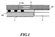
- Fig. 1 is a conventional example of a packaging structure which gives optical connection between an optical waveguide and an optical fiber.
- This example realizes a structure in which an optical fiber 2 is fixed onto a V-shaped groove of an Si substrate 3 and connected to an optical waveguide 1a of an optical component 1.
- the optical waveguide 1 and the V-grooved substrate 3 are automatically aligned by the surface tension of solder bonds 3-31.
- the optical fiber 2 can thus be accurately positioned by a V-groove 3a. Since the positions of the optical fiber 2 and the optical waveguide 1 need to be determined accurately, however, packaging becomes laborious.
- automatic alignment by the solder 3-31 is employed. To make the effect of surface tension during soldering work, optimization of the reflow conditions is required.
- Fig. 2 shows a conventional example of packaging an optical component having an electrode.
- An active optical component is frequently used in high speed optical transmission.
- electrical wirings, etc. should be integrated.
- a lead for taking out the electrode for connection to the outside should be formed.
- an arrayed 4-channel optical device (photodiode) 1-3 is mounted on an optical component 1. From there, electrodes 1-4 for bonding are extended, and then bonding wires 101, chip resistors 102, and the bonding wires 101 are further provided, followed by lead wires 3-30 of a package (packaging platform) 3.
- packaging of an optical component with integrated parts requires an electrode withdrawal structure and wire bonding.
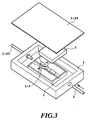
- Fig. 3 shows a conventional example of a hermetically sealed optical module.
- An optical device (laser diode) 1-3 forms an optical component 1 attached onto an Si substrate.
- On a package 3 as a packaging platform there are mounted an electric cable 3-40 for electric signal transmission and an optical fiber 2.
- the optical fiber 2 is fixed onto the Si substrate by a cover 5.
- a sealing cover 3-50 is hermetically applied such that the entire optical component 1 is sealed up, thereby providing a structure for a completely hermetic state.
- Such hermetic sealing requires a special container, making a packaging volume large.
- the use of the electric cable for electric signal transmission tends to lengthen the transmission distance.
- the resulting structure makes it difficult to accommodate a high frequency because of electric characteristics. As long as such a sealing form is taken, the more complicated the electrical wirings become, the larger the packaging volume and the worse the deterioration of signals will be.
- packaging of an optical component required the optical axis alignment of the optical waveguide and the optical fiber, and the structure for taking out an electrode from a fine electrode. Moreover, strict sealing was required, thereby imposing a severe burden on packaging.
- connection between the optical waveguide and an optical fiber has so far required a high accuracy aligning apparatus or an advanced packaging technique for performing precision positioning, even when a fiber guide structure is used.
- Another example is the production of an optical switch utilizing a thermooptic effect, or an optical module having an active portion on an optical waveguide circuit, such as a hybrid optical module having an optical semiconductor device packaged on an optical waveguide substrate.
- This production has posed the problem of electrical connection as well as the above-mentioned optical fiber connection. That is, wire bonding is needed to connect the electrical wiring portion of the optical waveguide circuit to another part such as a package.
- wire bonding is needed to connect the electrical wiring portion of the optical waveguide circuit to another part such as a package.
- a high density electrical wiring is required of the optical module.
- the step of electrical connection, such as bonding the wiring onto a miniscule electrode pattern, is also complicated.
- the above hybrid optical module has further required sealing of the surroundings of the optical semiconductor device, and needed for this purpose the step of mounting a sealing cover.
- This method has caused problems such as an increased volume of the optical module, or an adverse influence on electrical signals due to an increased electrical wiring length associated with the increased volume.
- An object of the present invention is to provide a packaging platform which can simplify all packaging steps including electrical connection and sealing as well as optical connection in connecting one or more optical components to one or more optical fibers and can improve the dimensional accuracy of alignment, an optical module comprising the packaging platforms, and methods for producing the packaging platform and the optical module.
- the present invention is directed to a packaging platform for achieving optical coupling between one or more optical waveguides of an optical component having the optical waveguides and one or more optical fibers; the packaging platform including a reference structure portion for performing the horizontal and vertical positioning of the optical component, and a fiber positioning portion for inserting and holding the optical fiber and positioning the optical fiber at a position where the optical fiber is optically connected to the optical waveguide.
- an electrical wiring pattern may be provided at a position opposed to an electrode pad of the electrode pattern of the optical component when the optical component is positioned relative to the optical fiber.
- the optical component may have an optical device for optical connection to the optical waveguide of the optical component, and a depressed portion may be present at a position opposed to the optical device when the optical component is positioned relative to the optical fiber.
- the packaging platform there may be a plurality of the optical components, and the packaging platform may have reference structure portions for performing the horizontal and vertical positioning of these optical components relative to one another.
- the fiber positioning portion may be V-shaped or cylindrical in cross section.
- an insertion/removal structure for making the optical fiber insertible and removable may be formed.
- the reference structure portion of the platform and a portion of the optical component may be provided with fitting shape portions which are fitted to each other to position the optical component relative to the platform.
- the fitting shape portion may have a stepped shape, and the fitting shape portion of the optical component may be in such a shape as to be fitted to the stepped shape.
- At least one groove for escaping an excess adhesive may be formed in a mounting portion of the platform which the optical component contacts.
- the packaging platform may have a cover for holding the optical fiber in an arrayed state when fixed to the platform after the optical fiber is connected to the platform having the optical component mounted thereon.
- a polymer optical waveguide circuit may be packaged on the platform.
- the packaging platform may be composed of a synthetic resin composition.
- this synthetic resin composition has a mold shrinkage coefficient of not more than 1%, and the shrinkage coefficient is isotropic, or the ratio of its maximum value to its minimum value is not more than 1.5.
- the synthetic resin composition may consist essentially of a thermosetting resin and may contain an inorganic filler.
- the thermosetting resin may be an epoxy resin.
- the inorganic filler may be a silica powder.
- the synthetic resin composition may consist essentially of an amorphous polymer and may contain an inorganic filler.
- the inorganic filler may be an inorganic crystalline powder, or an inorganic glass powder, or a mixture of these.
- the amorphous polymer may be polyethersulfone, polysulfone, polyetherimide, or a mixture of these.
- the packaging platform may be formed of a ceramic material.
- the packaging platform may be produced using a mold, and molding with this mold may be injection molding or transfer molding.
- Another packaging platform of the present invention may comprise a packaging platform for achieving optical coupling between one or more optical fibers and one or more optical waveguides of one or more optical components having the optical waveguide and/or an optical receiving device and/or an optical emitting device and an electrical circuit for controlling the optical device; the packaging platform including a reference structure portion for performing the horizontal and vertical positioning of the optical, component, and a fiber positioning portion for inserting and holding the optical fiber and positioning the optical fiber at a position where the optical fiber is optically connected to the optical waveguide.
- the optical module of the present invention may comprise an optical component and an optical fiber packaged on the packaging platform of the foregoing configuration.
- the optical fiber of the optical module may have an optical connector mounted thereon.
- Another optical module of the present invention may comprise an optical component having an optical waveguide and an electrode pattern, and also having a height reference surface provided at a position apart by a predetermined height from a core portion on the surface of the optical waveguide, and a horizontal reference structure portion provided at a position apart by a predetermined distance from the core portion; and a packaging platform having a height reference surface for determining the altitudinal position of the optical component on the platform and a horizontal reference structure portion for determining the horizontal position of the optical component on the platform, and also having a fiber positioning portion for inserting and holding an optical fiber and positioning the optical fiber at a position where the optical fiber is optically connected to the optical waveguide of the optical component, and an electrical wiring pattern provided at a position opposed to one or more electrode pad of the electrode pattern on the optical component; in which the horizontal reference structure portions of the optical component and the packaging platform may be aligned with each other, and the height reference surfaces of the optical component and the packaging platform may be brought into contact with each other, whereby the alignment and electrical connection of the electrode
- the optical component may have an optical device to be optically connected to the optical waveguide of the optical component, and the packaging platform may be further provided with a depressed portion at a position opposed to the optical device when the optical component is positioned relative to the optical fiber.
- the packaging platform may be further provided with a reference structure portion for performing the horizontal and vertical positioning of the optical components relative to one another.
- the horizontal reference structure portion may be a wall surface prepared by etching a cladding portion of the optical waveguide of the optical component, or may be a rib-shaped protrusion formed in the optical component. This rib-shaped protrusion may be the optical waveguide shaped like a rib of the optical component.
- the height reference surface of the optical component may be an exposed substrate surface formed when the cladding portion of the optical waveguide of the optical component has been removed to expose the substrate surface.
- the horizontal reference structure portion of the optical component may be a pair of engagement surfaces formed obliquely in the cladding portion of the optical waveguide of the optical component in the longitudinal direction of the optical waveguide, while the horizontal reference structure portion of the packaging platform may be a pair of engagement surfaces to come into contact with the pair of engagement surfaces of the optical component.
- the pair of engagement surfaces of the optical component may be placed at linearly symmetric positions with respect to an axis parallel to the optical axis of exit light from the optical waveguide.
- an insulating sealing resin may be filled into a gap between the optical component and the packaging platform. By adjusting the size of the gap between the optical component and the packaging platform, penetration of the resin into a specific portion may be inhibited.
- sealing of the optical device may be achieved by filling an insulating and transparent resin into the depressed portion.
- the packaging substrate may be composed of a synthetic resin composition
- the mold shrinkage coefficient of the synthetic resin composition may be not more than 1%
- the shrinkage coefficient may be isotropic or the ratio of its maximum value to its minimum value may be not more than 1.5.
- the synthetic resin composition may consist essentially of a thermosetting resin and may contain an inorganic filler.
- the thermosetting resin may be an epoxy resin.
- the inorganic filler may be a silica powder.
- the synthetic resin composition may consist essentially of an amorphous polymer and may contain an inorganic filler.
- the inorganic filler may be an inorganic crystalline powder, or an inorganic glass powder, or a mixture of these.
- the amorphous polymer may be polyethersulfone, polysulfone, polyetherimide, or a mixture of these.
- the packaging platform may be formed of a ceramic material.
- the fiber positioning portion may be V-shaped or cylindrical in cross section.
- an insertion/removal structure for making the optical fiber insertible and removable may be formed in the fiber positioning portion.
- a method for production of an optical module of the above-described configuration comprises packaging the optical component on the platform, connecting the optical fiber to the optical component, and then sealing an upper part or the whole of the platform with a resin mold.
- the present invention has aimed at attaining the aforementioned object.
- the invention has completed high accuracy alignment concerned with fiber connection, electrical connection and simplified sealing method, simply by installing an optical components on a packaging platform having a guide structure for simplifying positioning.
- the invention discloses the structure of a packaging platform, and provides the constitution of an optical module using this packaging platform.
- the invention also provides methods for producing the packaging platform and the optical module.
- an optical fiber positioning groove and an electrical wiring pattern are provided at certain distances from a horizontal reference structure portion and a vertical reference structure portion on the platform.
- horizontal and vertical reference structure portions corresponding to the reference structure portions on the packaging platform are provided, and an optical waveguide and an electrode pattern are provided at predetermined distances from these reference structure portions.
- the reference structure portion may have a planar, linear or punctate structure. That is, a reference surface, a reference line or a reference point is used for positioning.
- the reference surface refers to a flat or curved surface.
- the reference line refers to a ridgeline portion of a protuberant structure.
- the reference point means an apical portion of a protuberant structure.
- the reference line and the reference point may be marks printed in a linear and a punctate form, respectively. The mark is suitable in performing positioning by optical reading.
- the punctate reference structure portion may be a perforation.
- the reference line also includes a case in which positioning is carried out by a virtual surface formed by a row of ridgelines of a V-shape or corrugated form.
- the reference point also includes a case in which positioning is carried out along a virtual surface formed by an arrangement of pyramidal or conical apices.
- the horizontal reference structure portion of the optical component may be formed of a pair of engagement surfaces which are obliquely processed parts of the optical waveguide cladding portion.
- the horizontal reference structure portion of the packaging platform may be a pair of engagement surfaces corresponding to the engagement surfaces which make up the horizontal reference structure portion of the optical component.
- the two oblique engagement surfaces of the optical component may be disposed at linearly symmetrical positions with respect to an axis parallel to the optical axis of light leaving the optical waveguide.
- the shaded area corresponds to the reference structure portion of an optical component (or a packaging platform).
- a triangle DEF and a triangle ABC formed by extending the edges of the optical component ⁇ and the packaging platform ⁇ , respectively.
- the triangles DEF and ABC are designed as similar triangles by setting the angles ⁇ and ⁇ of both triangles to be the same.
- the side AB agrees with the side DE
- the side CA agrees with the side FD, automatically. That is, the reference portions of ⁇ and ⁇ come into agreement. Since the triangles ABC and DEF are similar to each other, the straight lines l and l' illustrated in the drawings also agree.
- Fig. 4B shows the edges of the packaging platform ⁇ receding by the distance w.
- the triangle ABC corresponds to a new triangle A'B'C'. Since the changes in this case are uniform, however, the new triangle keeps the feature of being similar to the triangle DEF.
- the angles ⁇ and ⁇ remain equal, the position of the reference line l is unchanged, and the optical fiber and the optical waveguide can be aligned as described above.
- Fig. 4C the same is true when the edges of the optical component ⁇ recede.
- the gap between the optical component and the packaging platform may be filled with an insulating and transparent or opaque sealing resin.
- the electrical wiring pattern provided on the packaging platform of the present invention is usually used to transmit signals to the electrical circuit piece parts mounted on the optical component, or drive or modulate the light detecting and emitting devices.
- the electrical wiring can be formed by various methods such as a molding method including a lead frame structure, or a method of circuit formation by MID when using injection molding.
- the fiber positioning portion on the packaging platform of the invention may be cylindrical in shape.
- This cylindrical structure allows alignment while inserting an optical fiber, and desirably has a cylinder with a slightly larger diameter than the fiber diameter.
- the input of the cylindrical structure through which the fiber is inserted should desirably constitute a tapered guide having a considerably larger diameter than the fiber diameter.
- the packaging platform of the invention brings more advantages when composed of a synthetic resin composition.
- the synthetic resin composition referred to here may be a thermoplastic resin or thermosetting resin alone or in combination with a filler. Alternatively, it may be a laminate of a synthetic resin and other material.
- the composition may be selected in the light of the environment in which the packaging platform is actually used.
- the packaging platform is required to have high dimensional accuracy, environment resistance (resistance to temperature, humidity or the like), and certain mechanical strength.
- the packaging platform is required to be minimal in size changing during processing, high in heat resistance and humidity resistance, and high in strength and modulus of elasticity.
- the platform is fabricated, most commonly, by the use of a precision processed mold, but can be prepared by precisely machining a plate material.
- the mold shrinkage coefficient of the synthetic resin composition is not more than 1%, and is isotropic or the ratio of its maximum value to its minimum value is not more than 1.5.
- a more concrete embodiment of the synthetic resin composition that realizes the dimensional accuracy required for the packaging platform of the invention is such that mold shrinkage during the molding of the synthetic resin composition is as low as possible and its anisotropy is reduced.
- the values of physical properties related to molding can be made isotropic.
- a thermoplastic resin is used, on the other hand, it is difficult to make the values of physical properties related to molding isotropic.
- the use of a resin composition having an anisotropy ratio of the shrinkage coefficient of not more than 1.5 gives a packaging platform with excellent characteristics. This has been clarified by the present invention. It has also been made clear that a mold shrinkage coefficient of not more than 1% can provide a product with little variation in dimensional values.
- thermosetting resin in this constitution are phenolic resin, unsaturated polyester resin, epoxy resin, diallyl phthalate resin, silicone resin, and melamine resin.
- inorganic filler examples include talc, mica, calcium carbonate, clay, alumina, alumina silica, silica, zinc oxide, carbon, aluminum hydroxide, asbestos fiber, glass fiber, and carbon fiber.
- epoxy resin may be used as the thermosetting resin.
- the epoxy resin referred to here is one which undergoes minimal size changing during processing, has high thermal resistance, and is high in strength and modulus of elasticity.
- Preferred examples of the epoxy resin are epoxy resins comprising epoxy resin precursors of the chemical formulae 1-1 to 1-29 and curing agents of the chemical formulae 2-1 to 2-6 as shown below.
- the ratio of the epoxy resin to the curing agent is preferably such that the ratio of the glycidyl groups in the epoxy resin to the hydroxyl groups in the curing agent is 1:1.
- a publicly known material such as an imidazole, an organophosphine compound, a urea derivative, or a phenolic novolak salt may be used as the curing promotor. Desirably, it is a material capable of improving stability at a temperature of about 100 °C at which injection molding becomes possible.
- the amount of silica powder added as the inorganic filler should desirably be not less than 30% by weight.
- Amorphous polymers are also preferred as the synthetic resin composition. Desirable examples of such polymers are polyethersulfone, polysulfone, polyetherimide, and mixtures of these.
- polyetherimide polyetherimides of the structures indicated in chemical formulae 3-1 to 3-4 shown below can be used.
- polyethersulfone polyethersulfones of the structures indicated in chemical formulae 4-1 to 4-5 shown below can be used.
- the optical connector mounted on the optical fiber constituting the optical module is an optical fiber-packaged device, such as MT, MU, MPO or SC, which has at the terminal portion of the optical fiber a structure capable of optical coupling to a packaging platform.
- an optical fiber-packaged device such as MT, MU, MPO or SC
- the optical device placed on the optical component is disposed in the depressed portion provided in the packaging platform, simply by putting together the reference structure portion of the packaging platform and the reference structure portion of the optical component.
- a state of a sealing cover being capped on the optical device can be realized substantially. That is, a single simple step can achieve all of fiber connection, electrical connection, and sealing.
- the horizontal reference structure portion of the optical component may be formed of two oblique engagement surfaces which are obliquely processed parts of the optical waveguide cladding portion.
- the horizontal reference structure portion of the packaging platform may be oblique engagement surfaces corresponding to the engagement surfaces of the optical component.
- the two oblique engagement surfaces of the optical component may be disposed at linearly symmetrical positions with respect to an axis parallel to the optical axis of light leaving the optical waveguide.
- the gap between the optical component and the packaging platform excluding the depressed portion may be filled with an insulating sealing resin.
- the depressed portion can show the function of hermetically sealing the optical device. Sealing of the optical device may be achieved by filling an insulating and transparent or opaque resin into the depressed portion. This measure enhances the sealing effect.
- optical connection between the optical waveguides present in the plurality of optical components can be achieved simply.
- the horizontal reference structure portion of the optical component may be formed of two oblique engagement surfaces which are obliquely processed parts of the optical waveguide cladding portion.
- the horizontal reference structure portion of the packaging platform may be oblique engagement surfaces corresponding to the engagement surfaces of the optical component.
- the two oblique engagement surfaces of the optical component may be disposed at linearly symmetrical positions with respect to an axis parallel to the optical axis of light leaving the optical waveguide.
- the gap between the optical component and the packaging platform may be filled with an insulating sealing resin.
- the resin for used in the resin mold used in the method of producing the optical module of the invention is not restricted.
- a publicly known sealing material for various electronic circuits may be used.
- the optical connector mounted on the optical fiber constituting an optical module of claim 28 of the invention is an optical fiber-packaged device, such as MT, MU, MPO or SC, which has at the terminal portion of the optical fiber a structure capable of optical coupling to a packaging platform.
- the optical device placed on the optical component is disposed in the depressed portion provided in the packaging platform, simply by putting together the reference structure portion of the packaging platform and the reference structure portion of the optical component.
- a state of a sealing cover being capped on the optical device can be realized substantially. That is, a single simple step can achieve all of fiber connection, electrical connection, and sealing.
- the horizontal reference structure portion of the optical component may be formed of two oblique engagement surfaces which are obliquely processed parts of the optical waveguide cladding portion.
- the horizontal reference structure portion of the packaging platform may be oblique engagement surfaces corresponding to the engagement surfaces of the optical component.
- the two oblique engagement surfaces of the optical component may be disposed at linearly symmetrical positions with respect to an axis parallel to the optical axis of light leaving the optical waveguide.
- the gap between the optical component and the packaging platform excluding the depressed portion may be filled with an insulating sealing resin.
- the depressed portion can show the function of hermetically sealing the optical device. Sealing of the optical device may be achieved by filling an insulating and transparent or opaque resin into the depressed portion. This measure enhances the sealing effect.
- optical connection between the optical waveguides present in the plurality of optical components can be achieved simply.
- the horizontal reference structure portion of the optical component may be formed of two oblique engagement surfaces which are obliquely processed parts of the optical waveguide cladding portion.
- the horizontal reference structure portion of the packaging platform may be oblique engagement surfaces corresponding to the engagement surfaces of the optical component.
- the two oblique engagement surfaces of the optical component may be disposed at linearly symmetrical positions with respect to an axis parallel to the optical axis of light leaving the optical waveguide.
- the gap between the optical component and the packaging platform may be filled with an insulating sealing resin.
- the resin for used in the resin mold used in the method of producing the optical module of claim 52 of the invention is not restricted.
- a publicly known sealing material or resin for mold packaging for various electronic circuits may be used.
- a packaging platform 11 was an injection molded article, which was composed of a concave structure (reference structure portion) 12 for inserting, positioning and fixing an optical component, V-groove portions 13, 13' (fiber positioning portions) capable of holding in an arrayed optical fibers for input and output of light into and from the optical component, and connecting the optical fibers to the optical component, and concave portions 14, 14' for accommodating and fixing the coating of the optical fiber ribbon enclosing a multiplicity of optical fibers.
- a concave structure reference structure portion
- V-groove portions 13, 13' fiber positioning portions
- Tables 1 and 2 show the specifications for the mold and the injection molding conditions.
- the resin used in molding was silica-containing epoxy resin. This epoxy resin was composed of 100 parts by weight of phenolic novolak type epoxy resin, 45 parts by weight of phenolic novolak resin, 15 parts by weight of a curing promotor, and 700 parts by weight of silica powder.
- the V-groove portions 13, 13' had a width of 140.3 ⁇ m, a groove depth of 121.5 ⁇ m, a groove angle of 60 degrees, and a groove interval of 250 ⁇ m.
- the dimensional accuracy of the mold was ⁇ 0.1 ⁇ m. Optical and mechanical measurements showed that the desired shape could be made with an accuracy of ⁇ 1 ⁇ m.
- the mold shrinkage was within 0.1%.
- a publicly known material such as an imidazole, an organophosphine compound, a urea derivative, or a phenolic novolak salt may be used as the curing promotor. Desirably, it is a material capable of improving stability at a temperature of about 100°C at which injection molding becomes possible.
- Mold specifications Item Specification Number of moldings One Method of temperature control Heating with heater Type of gate Side gate Runner Cold runner Number of plates Two Injection molding conditions Item Conditions Molding material Thermosetting epoxy resin Resin drying 30°C, 2 days Molding machine Thermosetting injection molding machine Clamping force: 35 tons Screw diameter: 25 mm Cylinder temp. Nozzle portion: 40°C Intermediate portion: 50°C Rear portion: 90°C Mold temp. 170°C Injection time 20 sec Curing time 20 sec Screw speed 80 rpm Screw back pressure 7 kg/cm 2 Injection pressure 250 kg/cm 2
- the flat portion and the flat portion in the guide groove could be brought into agreement in terms of height with an accuracy within 0.5 ⁇ m. That is, the concave structure 12 was produced with a dimensional accuracy of ⁇ 1 ⁇ m together with the V-groove portions 13, 13'. The size of the mold was designed in complete agreement with the dimensions of the light input and output portions of an optical component to be inserted into 12.
- This packaging platform could be produced with the same accuracy by transfer molding, and no difference in function was observed in the resulting two package platforms.
- a packaging procedure using the packaging platform 11 will be described concretely herein.
- Four-fiber optical fiber ribbons 16, 16' were connected to both ends of an optical waveguide circuit 15 prepared from a polymeric resin material in this Embodiment, whereby an optical module could be easily produced.
- the optical waveguide circuit 15 was inserted into the concave structure 12 of the packaging platform 11 and bonded with adhesive.
- the material for the covers 17, 17' may be glass, quartz or metal, but covers molded from resin were used in this embodiment.
- the covers 17, 17' had tiny protrusions 18, 18' on both side walls thereof, which were to be fitted into tiny recesses 19, 19' formed in both inner side walls of the packaging platform 11.
- the optical fiber ribbons 16, 16' could be positioned easily.
- the covers 17, 17' also had four tiny protuberances 20 in a direction along optical fibers in order to ensure the positioning of the optical fibers.
- the optical fibers could be fixed easily.
- the optical fiber ribbons 16, 16' can be fixed only by the fitting of the covers 17, 17'. To ensure reliability, however, a thermosetting adhesive was used in this embodiment for reliable fixation.
- the heat curing conditions were 90°C for 2 hours (primary curing) and 140°C for 3 hours (secondary curing).
- the fixation of the optical fiber ribbons 16, 16' can be performed using ultraviolet curing resin by preparing the covers 17, 17' made from transparent resin.
- This use of the packaging platform 11 enabled optical fiber ribbons to be connected together rapidly, correctly and reliably.
- the so produced optical module had a connection loss of 5.1 dB on the average, and involved no alignment procedure. Thus, a marked decrease in the operating time was possible.
- the entire packaging platform was sealed with resin, and the sealed product was examined for connection reliability by high temperature high humidity test (70°C, 90%). Even after passage of 2,000 hours, changes in connection characteristics were within 10%, confirming full reliability. Packaging of the entire packaging platform with a resin mold instead of a resin seal also demonstrated the same reliability.
- the second embodiment of the invention is shown in Fig. 6.
- the tiny protrusions 18, 18' were omitted in the covers 17, 17' of Embodiment 1, and optical fiber ribbons 16, 16' were pressed with metallic spring piece parts 50, 50'.
- exactly the same results as in Embodiment 1 were obtained for connection loss characteristics and reliability.
- Embodiment 1 corresponded to Embodiment 1 in which a silica optical waveguide circuit was used as the optical component.
- the same connection loss characteristics and reliability of the packaging platform as in Embodiments 1 and 2 were confirmed.
- o-cresol novolak resin was used instead of phenolic novolak resin as the starting material, the same results were also obtained.
- Fig. 7 shows the fourth embodiment of the invention. This embodiment involved only one input/output end of an optical component.
- a packaging platform 61 as in Embodiment 1, was composed of a concave structure 62 for inserting, positioning and fixing an optical component, a V-groove portion 63 capable of holding and connecting optical fibers in an array, and a concave portion 64 for accommodating and fixing the coating of an optical fiber ribbon 16 enclosing a multiplicity of optical fibers.
- the V-groove portion 63 and the concave portion 64 for fixing the optical fibers are formed only at one end.
- the materials used were the same as in Embodiments 1, 2 and 3.
- An optical component 65 was a hybrid optical component comprising semiconductor lasers (LD's), semiconductor laser output monitoring photodiodes (PD's), and signal detecting photodiodes placed in combination on a silica optical waveguide circuit. The optical input/output end of this product was only one.
- LD's semiconductor lasers
- PD's semiconductor laser output monitoring photodiodes
- signal detecting photodiodes placed in combination on a silica optical waveguide circuit. The optical input/output end of this product was only one.
- the packaging procedure was the same as in Embodiment 1, and the same connection loss characteristics and reliability of the packaging platform were confirmed.
- FIG. 8 shows the fifth embodiment of the invention.
- a module of this embodiment is characterised that an optical component 65 is comprised by forming a semiconductor lasar arry 65a and electrodes 65b on a Si substrate.
- the other constitution are the same as Embodiment 4, as well as materials used in the embodiment and a method for proceedinging the module are the same as Embodiment 4.
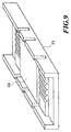
- Figs. 9 and 10 show an optical module related to the sixth embodiment of the invention.
- This embodiment as illustrated in Fig. 9, comprised an injection molded packaging platform 21, and an optical component 22 inserted into and fixed by adhesive to the packaging platform 21.
- a concave structure (reference structure portion) 23 for positioning and fixing V-groove portions (fiber positioning portions) 24, 24' capable of holding and connecting optical fibers in an array
- concave portions 25, 25' for accommodating and fixing the coating of optical fiber ribbons enclosing a multiplicity of optical fibers
- grooves 26, 26', 26'' provided in the concave structure 23 for accommodating excess adhesive.
- the specifications for a mold and the injection molding conditions for fabricating the packaging platform 21 were exactly the same as in the aforementioned Tables 1 and 2.
- the resin used in molding was silica-containing epoxy resin.
- the dimensions of the grooves 26, 26', 26'' provided in the concave structure 23 for accommodating excess adhesive were 200 ⁇ m in width and 300 ⁇ m in depth from the concave structure 23.
- the V-groove portions 24, 24' had a width of 140.3 ⁇ m, a guide groove depth of 121.5 ⁇ m, a guide groove angle of 60 degrees, and a guide groove interval of 250 ⁇ m.
- the dimensional accuracy of the mold was set at ⁇ 0.1 ⁇ m. Thus, the desired shape could be made with an accuracy of ⁇ 1 ⁇ m.
- the concave structure 23 was prepared with a dimensional accuracy of 1 ⁇ m, like the V-groove portions 24, 24', and could be molded in agreement with the dimensions of the light input and output portions of the optical component 22 to be inserted into the concave structure 23.
- the polymer optical component relevant to the instant embodiment was prepared by the following packaging procedure:
- the optical component 22 was placed on the packaging platform 21 shown in Fig. 9.
- the optical component 22 was a polymer optical waveguide including a 4 ⁇ 4 optical star coupler.
- This polymer optical waveguide was in a film form, and prepared in accordance with a method of forming a polymer optical waveguide circuit comprising a core and a cladding on a substrate having copper as a top layer, and then dipping this composite in an aqueous solution of hydrochloric acid to strip the polymer optical waveguide circuit portion from the substrate (Japanese Patent Application No. 127414/95).
- the core material was prepared from deuterated PMMA, and the cladding was produced from UV curable epoxy resin.
- the core size was 40 ⁇ m square, the distance from the bottom surface of the cladding to the core center was 75 ⁇ m, and the entire thickness was 150 ⁇ m.
- the polymer optical waveguide was cut to a size of -5 ⁇ m ⁇ 3 ⁇ m widthwise, and -10 ⁇ m ⁇ 5 ⁇ m lengthwise, relative to concave structure 23 of the packaging platform 21.
- the UV curing adhesive was inserted through the groove 26', and the polymer waveguide 22 was lightly pressed from above with a metal piece 1 mm smaller in width and length than the polymer waveguide 22 to bring the polymer waveguide 22 and the concave structure 23 of the packaging platform 21 into intimate contact.
- the so prepared polymer optical component can be connected, with desired characteristics, to a four-fiber optical fiber ribbon, and an optical packaged product can be produced easily.
- a pair of optical fiber ribbons were deprived of the coatings provided at the end, and were arranged and held in the V-groove portions 24, 24'.
- connection loss was evaluated using a laser light source having a wavelength of 0.85 ⁇ m and a photodiode. The connection loss was about 0.5 dB, thus permitting easy connection with low connection loss fibers.
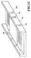
- Fig. 11 shows a polymer optical component related to the seventh embodiment of the invention.
- the polymer optical component of this embodiment comprised an injection molded packaging platform 27, and a polymer waveguide 28 inserted into the packaging platform 27 and having two sets of Y-branching waveguides fixed by adhesive to the packaging platform 27.
- the packaging platform 27 was the same as shown in Fig. 10 and prepared by the same method as described in Embodiment 6.
- the polymer optical component relevant to the instant embodiment was produced by the following packaging procedure:
- the polymer waveguide 28 having the two sets of Y-branching waveguides was placed on the packaging platform 27.
- This polymer optical waveguide was in a film form, and prepared in accordance with a method of forming a polymer optical waveguide circuit comprising a core and a cladding on a substrate having copper as a top layer, and then dipping this composite in an aqueous solution of hydrochloric acid to strip the polymer optical waveguide circuit portion from the substrate (Japanese Patent Application No. 127414/95).
- the core material was prepared from deuterated PMMA, and the cladding was produced from UV curable epoxy resin.
- the core size was 40 ⁇ m square, the distance from the bottom surface of the cladding to the core center was 75 ⁇ m, and the entire thickness was 150 ⁇ m.
- the polymer optical waveguide was cut to a size of -5 ⁇ m ⁇ 3 ⁇ m widthwise, and -10 ⁇ m ⁇ 5 ⁇ m lengthwise, compared with concave structure of the packaging platform.
- a UV curing adhesive was inserted through a groove 29, and the polymer waveguide 28 was lightly pressed from above with a metal piece 1 mm smaller in width and length than the polymer waveguide 28 to bring the polymer waveguide and the concave structure of the packaging platform 27 into intimate contact.
- the so prepared polymer optical component can be connected, with desired characteristics, to a four-fiber optical fiber ribbon, and an optical packaged product can be produced easily.
- the two optical fibers at the center of the four fibers of a four-fiber optical fiber ribbon were connected to the cores of the polymer waveguide on the input side of the two branches.
- the four optical fibers of another four-fiber optical fiber ribbon were connected to the four cores of the polymer waveguide located on the output side.
- the pair of optical fiber ribbons were pressed against the V-groove portions by press covers of glass from above.
- An ultraviolet curing adhesive was flowed into the V-groove portions to adhere and fix the optical fiber ribbons to the optical packaging component of the instant embodiment having the polymer waveguide mounted thereon.
- connection loss was evaluated using a laser light source having a wavelength of 0.85 ⁇ m and a photodiode. The connection loss was about 0.5 dB, thus permitting easy connection with low connection loss fibers.
- the two waveguides of the Y-branching devices were also confirmed to contain input light in a nearly 1:1 branched state.
- a polymer optical waveguide as a branching waveguide or a star coupler for branching and merging light regardless of its wavelength.
- an optical waveguide circuit having a demultiplexing function and a multiplexing function may be mounted, such as a Mach-Zehnder interferometer or an arrayed waveguide grating which has strongly wavelength-dependent branching/merging characteristics.
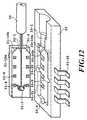
- Figs. 12, 13 and 14 are perspective views showing a packaging platform and an optical module using it, as the seventh embodiment of the present invention.
- the materials used were the same as in Embodiment 1, and molded by injection molding. All the dimensional accuracies were within ⁇ 1 ⁇ m.
- the numeral 33 denotes a packaging platform composed of a fiber positioning groove 33-1, a protruding guide 33-10, and leads 33-30 using lead frames as electrical wirings.
- the upper surface 33-10a served as a height reference surface, while its oblique side surface 33-10b constituted a horizontal reference surface (engagement surface).
- the position and dimensions of the fiber positioning groove 33-1 were set at predetermined values accurate to about 1 ⁇ m relative to the height reference surface 33-10a and the horizontal reference surface 33-10b.
- the position of the core center of the optical fiber 32 can be determined with an accuracy of about 1 ⁇ m relative to the height reference surface 33-10a and the horizontal reference surface 33-10b.
- the numeral 31 denotes an optical component which, concretely, had a silica optical waveguide comprising an optical waveguide core 31-1 and a cladding 31-2 on an Si substrate.
- the optical waveguide 31-1 constituted a straight waveguide
- a laser diode 31-3 was mounted on an optical device mounting portion formed by partially removing the cladding portion 31-2 by etching to make a laser optical module.
- an electrical wiring 31-4 for driving the laser diode 31-3 was provided, and a pad for electrical connection with the packaging platform 33 was provided forward of the electrical wiring.
- a radiating land 31-5 was provided for escaping heat to the packaging platform 33.
- the positional relationship of a horizontal reference surface 31-10b to the connecting pad of this electrical wiring pattern was set at a predetermined value accurate to about 1 ⁇ m.
- the cladding near the end of the optical waveguide substrate had been processed in an oblique form by removal by etching.
- This oblique engagement surface 31-10b functioned as a horizontal reference surface for the optical component 31, while a bottom surface 31-10a formed by etching functioned as a height reference surface.
- the horizontal position and height from the height reference surface to the optical waveguide core center were determined with an accuracy of about 1 ⁇ m relative to predetermined values.
- the positional relationship of the pad for the electrode pattern 31-32 to the horizontal reference surface was also determined with an accuracy of about 1 ⁇ m.
- the main constituents on the packaging platform 33 and the optical component i.e., optical fiber positioning groove 33-1, electrical wiring pattern 31-4, optical waveguide core 31-1, leads 33-30
- the optical component i.e., optical fiber positioning groove 33-1, electrical wiring pattern 31-4, optical waveguide core 31-1, leads 33-30
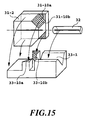
- Fig. 15 is a perspective view of the vicinity of the reference surface
- Fig. 16 is a plan view thereof
- Fig. 17 is a side view thereof.
- clad part of the both sides of the optical waveguide core of the optical component were processed in an oblique form, and the oblique engagement surfaces 31-10b were arranged linearly symmetrically with respect to an axis parallel to the optical axis of exit light from the optical waveguide.
- the drawing shows a case in which the linear symmetric axis and the optical axis agreed, but this agreement is not necessarily required. If excessive etching was done, the cladding portions on both sides would be equally scraped, and deviation of the axis of the optical waveguide from the optical axis would not occur.
- the alignment guide 33-10 for the packaging platform 33 was obliquely processed in agreement with 31-10. Clearly, this processing gives the same geometrical characteristics as in the optical waveguide substrate.
- FIG. 17 Alignment by the height reference surfaces 31-10a, 33-10a is illustrated in Fig. 17.
- the height reference surfaces 31-10a and 33-10a of the optical waveguide 31 and the packaging platform 33 were pressed against each other, whereby the positional relationship for height was determined between the height of the optical fiber 32 placed in the fiber positioning groove 33-1 and the height of the optical waveguide. If, based on this relationship, the distance of the optical waveguide core 31-1 from the height reference surface is conformed to the distance of the optical fiber core 32 from the height reference surface 31-10a, the heights of the optical fiber core 32-1 and the optical waveguide core 31-1 would agree.
- an optical waveguide including an electric circuit as in the embodiment shown in Figs.
- opposed electrical pads are formed in the optical waveguide 31 and the packaging platform 33, and an electrode withdrawing structure such as solder bumps 33-31 and 33-30 is used.
- an electrode withdrawing structure such as solder bumps 33-31 and 33-30 is used.
- the fixing of the optical component onto the packaging platform by means of solder bumps is performed by applying an adhesive or solder with the reference surfaces being pressed against each other, and holding this state until the adhesive or solder becomes cured.
- solder bumps is advantageous in that this holding step can be omitted. The reasons are illustrated in Fig. 18A.
- Fig. 18A is a sectional view of the area of bonding of a packaging platform 33 with solder bumps 33-31 to an optical component 31.
- the optical waveguide, optical fiber and optical device are not shown.
- the horizontal reference surface is a vertical wall running obliquely relative to the optical axis, but was indicated as a simple vertical wall for easy understanding. Alignment using the packaging platform 33 is performed by forcing the optical component 31 toward the packaging platform 33 in a downward, rightward direction on the sheet face of the drawing, and pressing the reference surfaces 31-10a and 33-10a against each other, and the reference surfaces 31-10b and 33-10b against each other.
- solder bumps 33-31 is accompanied, beforehand, by forming an electrode pad of the packaging platform 33 rightward of an electrode pad of the optical component 31, and adjusting the amount of the solder, so that the solder will pull the pad of the optical component 31 downward.
- the surface tension works, causing the optical component 31 to be automatically pressed in the downward, rightward direction on the sheet face of the drawing as shown in Figs. 18B and 18C.
- the optical component 31 and the packaging platform 33 can be fixed to each other with the reference surfaces in contact, without holding the optical component 31 by means of a packaging apparatus.
- the shape of the electrical pad or the solder bump may be inappropriate, or the surface of the solder bump may be oxidized and resistant to surface tension.
- the optical waveguide is held by a packaging apparatus or the like, the effect of surface tension can be suppressed and easy packaging is possible.
- the horizontal reference surface oblique relative to the optical axis was used.
- a horizontal reference surface parallel to the optical axis is present on each of the optical waveguide and the packaging platform, the high accuracy adjustment of the distance between the horizontal reference surface and the optical waveguide and between it and the optical fiber array structure would enable the optical axes of the optical waveguide and the optical fiber in the horizontal direction to be coaxial easily.
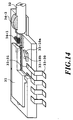
- the optical module illustrated in Figs. 13, 14, 15, 16 and 17 is an optical module after completion of assembly by a pigtail type optical fiber fixing method.
- the optical fiber 32 was placed on the fiber positioning portion 33-1 on the packaging platform 33.
- an adhesive 34-1 was put on the optical fiber 32 for fixation, and the coated portion of the optical fiber was fixed to the packaging platform 33 with an adhesive 34-2.
- the optical waveguide 31 was fixed by the use of an adhesive applied very thinly to the height reference surface 33-10 and solder bumps 33-31, although this is not shown.
- the optical waveguide 31 is pressed down toward the right on the sheet face of the drawing for fixation onto the packaging platform 33.
- the optical fiber can be aligned with the optical waveguide in the direction of height and on the horizontal plane as has been stated previously. Fixation then becomes possible without misalignment, as shown in Fig. 14 as a sectional view.
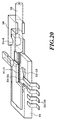
- Figs. 19 and 20 show an optical module of the type in which an optical fiber is inserted after mounting a packaging platform and an optical component to each other.
- Fig. 19 illustrates an assembled state
- Fig. 20 is a sectional view thereof.
- a press plate 35 with a V-groove adapted to fiber dimensions is fixed on a fiber positioning portion 33-1 to provide a hole-like structure for guiding a fiber 32.
- the optical fiber 32 can be inserted into the grooved portion 33-1 where necessary, to obtain optical coupling with an optical waveguide 31.
- a hook 36 was attached to the optical fiber, and a packaging platform 33 with a retiring part 33-6 to be fitted to the hook 36 was used to make a structure capable of detachable mounting of the optical fiber 32.
- Fig. 21 shows an example of a sealing structure of an optical module of the type in which a resin is poured between an optical waveguide substrate 31 and a packaging platform 33.
- This sealing method is effective in providing a seal for protection of an electrode, an electrical wiring, etc.
- the reason is as follows: To enhance a sealing effect, as small a sectional area of a resin layer as possible is desirable; the resin has some moisture permeability, so that the larger the sectional area of the resin layer, the easier the penetration of water molecules becomes.
- the packaging platform 33 substantially plays the role of a cover for the optical component, thus making it possible to thin a layer of resin to be penetrated into the gap. Because of this, the optical module of the invention enables sealing with resin to exhibit very high reliability.
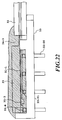
- the sealing resin may be a transparent resin or an opaque resin. When a transparent resin is used, it may be flowed into the junction between the optical fiber and the optical waveguide, and can function as a refractive index aligner as well as a sealant. This example is illustrated in Fig. 22.
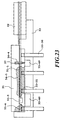
- Fig. 23 shows an example of an optical module sealed with resin injected into a gap between an optical waveguide substrate 31 and a packaging platform 33, constructed such that the resin does not enter a part of the gap.
- the resin has affinity for the optical waveguide substrate 31 and packaging platform 33.
- the embodiment utilized the feature of the sealing resin that because of surface tension, the resin naturally deforms into such a shape that its portion in touch with the air shrinks. This means a configuration in which flowing of the sealing resin into part of the gap is suppressed by providing the packaging platform 33 or the optical waveguide substrate 31 with a structure 33-40 for widening the gap between the optical waveguide substrate 31 and the packaging platform 33 by a sharp-angled difference in level.
- the sealing resin can be prevented from contacting the optical device, because of refractive index, etc., or can be prevented from escaping to an optical component, such as a film-shaped optical component 37, which is susceptible to influence from stress because of its shape.
- This embodiment has given consideration to a case in which the optical module may be heated, although not shown. To avoid the situation that a hollow surrounded by the resin may be formed in the gap, there was used a packaging platform of a structure in which there is no resin-surrounded portion by the use of a groove as shown in Figs. 9, 10 and 11.
- Fig. 24 shows the tenth embodiment of the present invention.
- the difference of this embodiment from Embodiments 8 and 9 is that positioning reference surfaces for a plurality of optical components were provided on a packaging platform.
- optical fibers 32, and optical components 31-a and 31-b by Y branching optical waveguides were placed on packaging platforms 33-a and 33-b, respectively.
- Positioning reference surfaces 33-10 for the two piece parts that connected the optical fibers 32 together were provided on the packaging platforms 33. These positioning reference surfaces are matched with positioning reference surfaces 31-10 provided on the optical components 31-a and 31-b, whereby alignment between the optical waveguides provided on both optical components can be realized.
- This embodiment was also constituted such that the positioning reference surfaces on the packaging platform were formed so that a gap would be formed between both optical components, and a film-shaped component 37 would be inserted into this gap.
- This film-shaped component 37 was an optical wavelength filter composed of a dielectric multilayer.
- an electrode pattern and a semiconductor optical device may be placed on the optical component, while an electrical wiring pattern and a depressed portion corresponding to them may be provided on the packaging platform. Furthermore, an optical fiber positioning groove portion for these optical components may be provided.
- a plurality of optical components can be combined into a large-scale optical module.
- alignment between the optical fiber and the optical waveguide, alignment between the optical waveguide and the optical waveguide, alignment between the electrode pattern and the electrical wiring pattern, and alignment between the semiconductor optical device and the depressed portion all can be accomplished by matching between the positioning reference surfaces on the packaging platform and the positioning reference surfaces on the optical component.
- Fig. 25 illustrates this method, according to which horizontal reference marks (punctate horizontal reference structure portions) 31-11 are formed on height reference surfaces 31-10a of an optical component 31.
- horizontal reference marks (punctate horizontal reference structure portions) 33-11 are formed on height reference surfaces 33-10a.
- the horizontal reference marks 33-11 are, say, through-holes.
- the material for the packaging platform may be a precision-processable one, and is not restricted to a particular material.
- the packaging platform may be formed from a material such as silicon or ceramic.
- the packaging platform molded from a resin material among wide varieties of feasible materials is markedly superior in terms of economy and mass producibility. Examples of such resin materials are thermosetting epoxy resins containing 50% of glass powder, and polyetherimide, polysulfone and polyethersulfone resins containing 40% of glass powder.
- the packaging platform was shaped like a housing of an optical waveguide substrate.
- the packaging platform may be in the form of a substrate extending on a plane.
- the first characteristic of the present invention lies in a structure in which alignment in optically coupling an optical component and an optical fiber with the use of a packaging platform can be performed accurately and easily.
- the second characteristic of the invention lies in providing a material constitution for actualizing the first characteristic in an optimal state.
- the instant Embodiment 12 and following Embodiments 13 to 17 disclose concrete examples of such a material constitution.
- the illustrated packaging platform 33 can perform the alignment of a single mode optical waveguide component 31 by the use of two opposed reference surfaces provided in the packaging platform 33 and the single mode optical waveguide component 31.
- the packaging platform 33 and the optical waveguide component 31 are both precisely formed so that when these opposed reference surfaces are brought into contact with each other, the cores of optical fibers agree with the cores of the single mode optical waveguide component 31.
- the required accuracy in this case is within ⁇ 0.5 micron relative to the target position.
- Quenched steel was precision processed to a dimensional accuracy of ⁇ 0.1 micron.
- the above composition was injection molded in the following manner using the above mold:
- the composition was fed to an injection molding machine having a clamping pressure of 50 tons, an injection capacity of 49 cm3 , a plastication capacity of 25 kg/hr, and an injection pressure of 1,750 kg/ cm2 , and molded under the conditions, a cylinder temperature of 50°C below the hopper and 90°C in the nozzle area, a mold temperature of 180°C, an injection time of 20 seconds, a curing time of 20 seconds, and an injection pressure of 750 kg/ cm2 .
- the molded material was post-cured for 3 hours at 180°C.
- the above-mentioned composition was molded by a transfer molding machine to obtain molded products having the same characteristics.
- An optical waveguide component was mounted at a reference surface position of the resulting molded product, and optical fibers polished at the end face were fixed to the optical waveguide component along the V-groove guides.
- the connection loss was 0.1 dB or less, thus confirming that precise alignment was realized.
- the illustrated packaging platform 33 can perform the alignment of a single mode optical waveguide component 31 by the use of two opposed reference surfaces (a flat surface in the optical waveguide component 31; a surface formed by connecting together the ridgelines 70 of the V-shapes at the bottom of the platform 33 in its sectional view).
- the packaging platform 33 and the optical waveguide component 31 are both precisely formed so that when these opposed reference surfaces are brought into contact with each other, the cores of optical fibers agree with the cores of the single mode optical waveguide component 31.
- the required accuracy in this case is within ⁇ 0.5 micron relative to the target position.
- Quenched steel was precision processed to a dimensional accuracy of ⁇ 0.1 micron.
- the above composition was injection molded in the following manner using the above mold:
- the composition was fed to an injection molding machine having a clamping pressure of 50 tons, an injection capacity of 49 cm 3 , a plastication capacity of 25 kg/hr, and an injection pressure of 1,750 kg/ cm2 , and molded under the conditions, a cylinder temperature of 50°C below the hopper and 90°C in the nozzle area, a mold temperature of 180°C, an injection time of 20 seconds, a curing time of 20 seconds, and an injection pressure of 750 kg/ cm2 .
- the molded material was post-cured for 3 hours at 180°C.
- the above-mentioned composition was molded by a transfer molding machine to obtain molded products having the same characteristics.
- An optical waveguide component was mounted at a reference surface position of the resulting molded product, and optical fibers polished at the end face were fixed to the optical waveguide component along the V-groove guides.
- the connection loss was 0.1 dB or less, thus confirming that precise alignment was realized.
- the illustrated packaging platform 33 can perform the alignment of a single mode optical waveguide component 31 by the use of two opposed reference surfaces (a flat surface in the optical waveguide component 31; a surface formed by connecting together the apices of conical shapes 71 in the platform 33).
- the packaging platform 33 and the optical waveguide component 31 are both precisely formed so that when these opposed reference surfaces are brought into contact with each other, the cores of optical fibers agree with the cores of the single mode optical waveguide component 31.
- the required accuracy in this case is within ⁇ 0.5 micron relative to the target position.
- Quenched steel was precision processed to a dimensional accuracy of ⁇ 0.1 micron.
- the above composition was injection molded in the following manner using the above mold:
- the composition was fed to an injection molding machine having a clamping pressure of 50 tons, an injection capacity of 49 cm3 , a plastication capacity of 25 kg/hr, and an injection pressure of 1,750 kg/ cm2 , and molded under the conditions, a cylinder temperature of 50°C below the hopper and 90°C in the nozzle area, a mold temperature of 180°C, an injection time of 20 seconds, a curing time of 20 seconds, and an injection pressure of 750 kg/ cm2 .
- the molded material was post-cured for 3 hours at 180°C.
- the above-mentioned composition was molded by a transfer molding machine to obtain molded products having the same characteristics.
- An optical waveguide component was mounted at a reference surface position of the resulting molded product, and optical fibers polished at the end face were fixed to the optical waveguide component along the V-groove guides.
- the connection loss was 0.1 dB or less, thus confirming that precise alignment was realized.
- the illustrated packaging platform 33 can perform the alignment of a single mode optical waveguide component 31 by the use of two opposed reference surfaces provided in the packaging platform 33 and the single mode optical waveguide component 31.
- the packaging platform 33 and the optical waveguide component 31 are both precisely formed so that when these opposed reference surfaces are brought into contact with each other, the cores of optical fibers agree with the cores of the single mode optical waveguide component 31.
- the required accuracy in this case is within ⁇ 0.5 micron relative to the target position.
- the diameter of each of cylinders 72 as inputs for optical fibers was set at 200 microns, while the diameter of each of cylinders 73 on the alignment side was set at 126 microns.
- the molding method for the packaging platform complied with the aforementioned Embodiment 12. As a result, molded products having a dimensional error of ⁇ 0.5 micron relative to the target value were obtained continuously.
- the aforementioned composition was molded by a transfer molding machine to obtain molded products having the same characteristics.
- optical waveguide component was mounted at a reference surface position of the resulting molded product, and optical fibers (125 microns in diameter) polished at the end face were fixed to the optical waveguide component along the cylindrical guides.
- the connection loss was 0.1 dB or less, thus confirming that precise alignment was realized.
- the illustrated packaging platform 33 can perform the alignment of a single mode optical waveguide component 31 by the use of two opposed reference surfaces provided in the packaging platform 33 and the single mode optical waveguide component 31.
- the packaging platform 33 and the optical waveguide component 31 are both precisely formed so that when these opposed reference surfaces are brought into contact with each other, the cores of optical fibers agree with the cores of the single mode optical waveguide component 31.
- the required accuracy in this case is within ⁇ 1 micron relative to the target position.
- Quenched steel was precision processed to a dimensional accuracy of ⁇ 0.1 micron.
- the above composition was injection molded in the following manner using the above mold:
- the composition was fed to an injection molding machine having a clamping pressure of 50 tons, an injection capacity of 49 cm 3 , a plastication capacity of 25 kg/hr, and an injection pressure of 1,750 kg/ cm2 , and molded under the conditions, a cylinder temperature of 50°C below the hopper and 90°C in the nozzle area, a mold temperature of 180°C, an injection time of 20 seconds, a curing time of 20 seconds, and an injection pressure of 750 kg/ cm2 .
- the molded material was post-cured for 3 hours at 180°C.
- the above-mentioned composition was molded by a transfer molding machine to obtain molded products having the same characteristics.
- An optical waveguide component was mounted at a reference surface position of the resulting molded product, and optical fibers polished at the end face were fixed to the optical waveguide component along the V-groove guides.
- the connection loss was 0.1 dB or less, thus confirming that precise alignment was realized.
- the illustrated packaging platform 33 can perform the alignment of a single mode optical waveguide component 31 by the use of two opposed reference surfaces provided in the packaging platform 33 and the single mode optical waveguide component 31.
- the packaging platform 33 and the optical waveguide component 31 are both precisely formed so that when these opposed reference surfaces are brought into contact with each other, the cores of optical fibers agree with the cores of the single mode optical waveguide component 31.
- the required accuracy in this case is within ⁇ 1 micron relative to the target position.
- a synthetic resin containing silica particles (average particle size 30 microns or less) in a varying proportion as shown in Table 5 based on polyetherimide resin.
- Silica (% wt/wt) Anisotropy Dimensional error Remarks 0 1.7 - Warping confirmed visually 30 1.3 ⁇ 1 ⁇ m
- Quenched steel was precision processed to a dimensional accuracy of ⁇ 0.1 micron.
- the above composition was injection molded using the above mold under the same conditions as described in the aforementioned embodiments.
- Figs. 32 and 33 shown an example of a packaging platform 80 using ceramic.
- the constitution of an optical module was almost the same as in Figs. 12 and 19.
- the structure of the lead and the alignment structure differed.
- the lead portion was composed of a lead frame. With ceramic, a burning step was involved. Thus, a high melting point metal such as tungsten was patterned and embedded. This pattern was gold plated, and then brazed to the lead.
- the alignment structure was worked out in consideration of a deviation from the mold due to deformation during sintering. Only an alignment reference surface 80-10a for alignment in the height direction was the surface as sintered. The reason is as follows: The main cause of deformation during ceramic sintering is shrinkage during sintering. The height-direction alignment reference surface of the packaging platform, if deformed, changes uniformly and can be used as a reference surface. Whereas a wall surface 80-10c, as a reference surface for alignment in the transverse direction, is located at a site apart from an optical waveguide component 31 and an optical fiber 32. This distance varies after sintering. Thus, a vertical wall surface 80-10d prepared by a precision dicing saw whose precision feeding was controllable was used as a reference surface for optical axis alignment in the transverse direction.
- Alignment in the height direction was performed upon contact of these reference surfaces with a height reference surface 31-10a of the optical waveguide component 31 and the surface of a V-groove substrate 35' attached to the optical fiber 32.
- the V-groove was formed by precision processing using the anisotropic etching of Si.
- the distance from the height reference surface of the optical waveguide component 31 was brought into agreement with the distance of the optical fiber core from the surface of the V-groove substrate 35' made of Si.
- Alignment in the transverse direction was performed by pressing a cladding wall surface, which was a transverse reference surface of the waveguide component 31, and a projecting side surface of the optical fiber 32 (projecting from the V-groove substrate 35') against the wall surface 80-10c formed by the above-mentioned dicing.
- a deviation of about several microns to 20 microns in the position of dicing would pose no problem.
- Of importance here would be the pitch of dicing. If this pitch is determined, precise alignment would become possible, because the distance from the transverse reference surface of the optical waveguide to the core of the optical waveguide, and the distance from the side surface of the optical fiber to the optical fiber core have been accurately determined.
- the pitch of dicing can be controlled to about 1 micron.
- the packaging platform of the present invention is a packaging platform for achieving optical coupling of an optical fiber to an optical waveguide of an optical component having the optical waveguide and an electrode pattern formed on the surface of the optical waveguide; the packaging platform including a planar, linear or punctate reference structure portion for performing the horizontal and vertical positioning of the optical component, and a fiber positioning portion for inserting and holding the optical fiber and positioning the optical fiber at a position where the optical fiber is optically connected to the optical waveguide of the optical component, and also including an electrical wiring pattern provided at a position opposed to one or more electrode pads of the electrode pattern on the optical component. Furthermore, a depressed portion may be provided at a position on the packaging platform opposed to an optical device carried on the optical component.
- the packaging platform of the invention has all of an optical fiber connecting function, an electrically connecting function, and a sealing function with an appropriate sealing material. Hence, the use of the packaging platform of the invention can markedly cut down on the number of the constituents of an optical module, thus enabling a low cost optical module to be produced.
- the packaging platform is combined with an optical component which has on its surface a positioning reference surface corresponding to a positioning reference surface of the packaging platform, and also has an optical waveguide, an electrode pattern and an optical device manufactured so that their positions and distances from the positioning reference surface will agree with those of the packaging platform.
- the invention simplifies the manufacturing procedure for an optical module, thus permitting a low cost optical module to be realized.
- the invention uses a resin molded product as a packaging platform, and employs for the usable resin a concrete resin composition as disclosed in the claims and Embodiments of the invention.
- a resin molded product as a packaging platform
- employs for the usable resin a concrete resin composition as disclosed in the claims and Embodiments of the invention.
- the packaging platform is composed of resin, so that its mass production by molding becomes possible, markedly reducing the manufacturing cost.
- a packaging platform (11, 21, 33, 61) for optically coupling one or more optical waveguides of one or more optical components (15, 22, 31, 65) having the optical waveguide to one or more optical fibers is provided with a reference structure portion (31-10a, 31-10b, 33-10a, 33-10b, 33-6, 80-10a, 80-10c, 80-10d) for the horizontal and vertical positioning of the optical component (15, 22, 31, 65) and one or more fiber positioning portions (33-1) for inserting and holding the optical fiber and positioning the optical fiber at a position where the optical fiber is optically connected to the optical waveguide; whereby the packaging platform (11, 21, 33, 61) and an optical module using the platform are provided which can simplify all alignment steps for optical coupling, electrical connection and sealing in the coupling of the optical component and the optical fiber.
Landscapes
- Physics & Mathematics (AREA)
- General Physics & Mathematics (AREA)
- Optics & Photonics (AREA)
- Optical Couplings Of Light Guides (AREA)
Applications Claiming Priority (9)
| Application Number | Priority Date | Filing Date | Title |
|---|---|---|---|
| JP5887697 | 1997-03-13 | ||
| JP5887697 | 1997-03-13 | ||
| JP58876/97 | 1997-03-13 | ||
| JP19808397 | 1997-07-24 | ||
| JP198083/97 | 1997-07-24 | ||
| JP19808397 | 1997-07-24 | ||
| JP2755898 | 1998-02-09 | ||
| JP27558/98 | 1998-02-09 | ||
| JP2755898 | 1998-02-09 |
Publications (2)
| Publication Number | Publication Date |
|---|---|
| EP0864893A2 true EP0864893A2 (fr) | 1998-09-16 |
| EP0864893A3 EP0864893A3 (fr) | 1999-09-22 |
Family
ID=27285842
Family Applications (1)
| Application Number | Title | Priority Date | Filing Date |
|---|---|---|---|
| EP98104508A Ceased EP0864893A3 (fr) | 1997-03-13 | 1998-03-12 | Plate-forme de montage, module optique avec ce module, et procédés de fabrication de la plate-forme et du module |
Country Status (2)
| Country | Link |
|---|---|
| US (1) | US6222967B1 (fr) |
| EP (1) | EP0864893A3 (fr) |
Cited By (17)
| Publication number | Priority date | Publication date | Assignee | Title |
|---|---|---|---|---|
| FR2773222A1 (fr) * | 1997-12-31 | 1999-07-02 | Samsung Electronics Co Ltd | Structure pour connecter des fibres optiques a un guide d'onde optique |
| EP0977061A2 (fr) * | 1998-07-28 | 2000-02-02 | Japan Aviation Electronics Industry, Limited | Dispositif à guide d'onde optique et sa méthode de fabrication |
| WO2000055665A2 (fr) * | 1999-03-16 | 2000-09-21 | Framatome Connectors International | Connecteur optoelectronique modulaire |
| WO2001006285A2 (fr) * | 1999-07-16 | 2001-01-25 | Hybrid Micro Technologies Aps | Integration hybride de composants optiques actifs et passifs sur une carte au silicium |
| WO2002031561A1 (fr) * | 2000-10-09 | 2002-04-18 | Siemens Aktiengesellschaft | Support pour composants optoelectroniques |
| WO2002054125A1 (fr) * | 2001-01-06 | 2002-07-11 | Corning Incorporpated | Alignement de composants de fibre optique |
| GB2386432A (en) * | 2002-03-11 | 2003-09-17 | Bookham Technology Plc | Sealed optic fibre package containing optics chip |
| WO2003103191A1 (fr) * | 2002-06-04 | 2003-12-11 | Iljin Corporation | Module optique multivoies |
| US6778718B2 (en) | 2001-11-09 | 2004-08-17 | Corning Incorporated | Alignment of active optical components with waveguides |
| EP1451620A2 (fr) * | 2001-10-01 | 2004-09-01 | Jeffrey M. Catchmark | Plate-forme d'encapsulation de composants optiques, opto-electroniques et electroniques |
| WO2004086111A1 (fr) * | 2003-03-24 | 2004-10-07 | Photon-X L.L.C. | Module optoelectronique a structure composite |
| EP1967878A1 (fr) * | 2005-12-28 | 2008-09-10 | OMRON Corporation, a corporation of Japan | Module optique |
| EP2169437A1 (fr) * | 2008-09-25 | 2010-03-31 | Fuji Xerox Co., Ltd. | Module optique, dispositif de transmission optique, et dispositif optique de surface |
| EP3043197A1 (fr) | 2015-01-08 | 2016-07-13 | Fraunhofer-Gesellschaft zur Förderung der angewandten Forschung e.V. | Systeme support pour elements fonctionnels de la micro-technique |
| CN110741294A (zh) * | 2017-06-07 | 2020-01-31 | 日本电信电话株式会社 | 光波导芯片的连接结构 |
| CN112327419A (zh) * | 2020-11-03 | 2021-02-05 | 中航光电科技股份有限公司 | 一种波导垂直光耦合结构 |
| CN114236689A (zh) * | 2021-12-23 | 2022-03-25 | 武汉锐科光纤激光技术股份有限公司 | 光学器件生产设备及光学器件的生产方法 |
Families Citing this family (55)
| Publication number | Priority date | Publication date | Assignee | Title |
|---|---|---|---|---|
| CN1208647C (zh) * | 1998-08-04 | 2005-06-29 | 住友电气工业株式会社 | 光组件插头用连接器、光组件制品以及光组件安装基板制品 |
| DE19964228B4 (de) | 1998-09-08 | 2008-11-13 | Fujitsu Ltd., Kawasaki | Verfahren zur Herstellung eines Reflexionsfilms und Herstellung optischer Vorrichtungen die einen Reflexionsfilm verwenden |
| US6588949B1 (en) * | 1998-12-30 | 2003-07-08 | Honeywell Inc. | Method and apparatus for hermetically sealing photonic devices |
| US6585427B2 (en) * | 1999-01-11 | 2003-07-01 | Intel Corporation | Flexure coupled to a substrate for maintaining the optical fibers in alignment |
| US6304695B1 (en) * | 1999-05-17 | 2001-10-16 | Chiaro Networks Ltd. | Modulated light source |
| US6792178B1 (en) | 2000-01-12 | 2004-09-14 | Finisar Corporation | Fiber optic header with integrated power monitor |
| JP4060023B2 (ja) * | 2000-03-28 | 2008-03-12 | 沖電気工業株式会社 | 光導波路送受信モジュール |
| US7046868B2 (en) | 2000-03-28 | 2006-05-16 | Oki Electric Industry Co., Ltd. | Optical waveguide transmitter-receiver module |
| US7345316B2 (en) * | 2000-10-25 | 2008-03-18 | Shipley Company, L.L.C. | Wafer level packaging for optoelectronic devices |
| US6839474B2 (en) * | 2000-11-16 | 2005-01-04 | Shipley Company, L.L.C. | Optical assembly for coupling with integrated optical devices and method for making |
| US6932519B2 (en) | 2000-11-16 | 2005-08-23 | Shipley Company, L.L.C. | Optical device package |
| US6827503B2 (en) * | 2000-12-01 | 2004-12-07 | Shipley Company, L.L.C. | Optical device package having a configured frame |
| US6883977B2 (en) * | 2000-12-14 | 2005-04-26 | Shipley Company, L.L.C. | Optical device package for flip-chip mounting |
| WO2002079843A1 (fr) * | 2001-03-28 | 2002-10-10 | Iljin Corporation | Module optique de type enfichable |
| WO2002079845A1 (fr) * | 2001-03-28 | 2002-10-10 | Iljin Corporation | Module optique petit équipé d'un guide d'ondes optique |
| US6788847B2 (en) * | 2001-04-05 | 2004-09-07 | Luxtera, Inc. | Photonic input/output port |
| US7078671B1 (en) * | 2001-08-06 | 2006-07-18 | Shipley Company, L.L.C. | Silicon optical microbench devices and wafer-level testing thereof |
| US7413688B2 (en) | 2001-09-17 | 2008-08-19 | Kenneth Noddings | Fabrication of optical devices and assemblies |
| EP1298474A1 (fr) * | 2001-09-27 | 2003-04-02 | Agilent Technologies, Inc. (a Delaware corporation) | Boítier pour composants opto-électriques |
| US6665475B2 (en) * | 2001-11-30 | 2003-12-16 | Jds Uniphase Corporation | Precision fiber optic alignment and attachment apparatus |
| KR20030065908A (ko) * | 2002-02-01 | 2003-08-09 | 주식회사 옵토*온 | 수동 및 능동정렬이 가능한 실리콘광학테이블 |
| US20030174963A1 (en) * | 2002-03-14 | 2003-09-18 | Brown Gordon C. | Strain optimized cantilever pigtail attach method with low moment staking |
| DE10211677B4 (de) * | 2002-03-15 | 2007-08-09 | Mergeoptics Gmbh | Anordnung zum Senden oder Empfangen von optischen Signalen |
| US7295742B2 (en) * | 2002-05-31 | 2007-11-13 | Matsushita Electric Industrial Co., Ltd. | Optical element and method for producing the same |
| US6907178B2 (en) * | 2002-06-13 | 2005-06-14 | Steve Lerner | Optoelectronic assembly with embedded optical and electrical components |
| US7426328B2 (en) * | 2002-08-28 | 2008-09-16 | Phosistor Technologies, Inc. | Varying refractive index optical medium using at least two materials with thicknesses less than a wavelength |
| US8538208B2 (en) * | 2002-08-28 | 2013-09-17 | Seng-Tiong Ho | Apparatus for coupling light between input and output waveguides |
| US6819841B2 (en) | 2002-08-29 | 2004-11-16 | International Business Machines Corporation | Self-aligned optical waveguide to optical fiber connection system |
| JP4145612B2 (ja) * | 2002-08-30 | 2008-09-03 | ユーディナデバイス株式会社 | 光学多層膜及びそれを有する光半導体装置 |
| US7229763B2 (en) * | 2003-04-07 | 2007-06-12 | Beckman Coulter, Inc. | Assay system using labeled oligonucleotides |
| US7499614B2 (en) * | 2003-10-24 | 2009-03-03 | International Business Machines Corporation | Passive alignment of VCSELs to waveguides in opto-electronic cards and printed circuit boards |
| US7077810B2 (en) | 2004-02-05 | 2006-07-18 | Earlysense Ltd. | Techniques for prediction and monitoring of respiration-manifested clinical episodes |
| JP2005352453A (ja) * | 2004-05-12 | 2005-12-22 | Nec Corp | 光ファイバ部品及び光導波路モジュール並びにこれらの製造方法 |
| US20050276612A1 (en) * | 2004-06-14 | 2005-12-15 | Debra Wawro | Opto-electronic module |
| JP4307344B2 (ja) * | 2004-07-20 | 2009-08-05 | シチズン電子株式会社 | 表面実装型モジュール |
| JP5186785B2 (ja) * | 2007-03-23 | 2013-04-24 | 日本電気株式会社 | 光導波路デバイス、光導波路デバイス用光素子実装システム、光素子実装方法、及びそのプログラム |
| CN101755403B (zh) * | 2007-07-12 | 2013-06-19 | 艾迪株式会社 | 具有集成光功率监控器的光纤阵列单元 |
| US8811778B2 (en) * | 2007-08-01 | 2014-08-19 | Hewlett-Packard Development Company, L.P. | Systems and method for routing optical signals |
| US11181688B2 (en) | 2009-10-13 | 2021-11-23 | Skorpios Technologies, Inc. | Integration of an unprocessed, direct-bandgap chip into a silicon photonic device |
| US9923105B2 (en) | 2013-10-09 | 2018-03-20 | Skorpios Technologies, Inc. | Processing of a direct-bandgap chip after bonding to a silicon photonic device |
| WO2011117808A1 (fr) * | 2010-03-22 | 2011-09-29 | Colorchip (Israel) Ltd. | Emetteur-récepteur opto-électronique avec boîtier à facteur de forme réduit |
| US8917963B2 (en) | 2010-05-21 | 2014-12-23 | Kaiam Corp. | MEMS-based levers and their use for alignment of optical elements |
| JP5956815B2 (ja) * | 2012-04-20 | 2016-07-27 | 日本航空電子工業株式会社 | 光モジュール用基体及び光モジュール |
| KR101493175B1 (ko) * | 2013-01-24 | 2015-02-12 | 가부시키가이샤후지쿠라 | 광결합 방법 및 커넥터 부착 케이블의 제조방법 |
| US9947636B2 (en) | 2014-06-02 | 2018-04-17 | Stmicroelectronics, Inc. | Method for making semiconductor device with lead frame made from top and bottom components and related devices |
| US9165867B1 (en) | 2014-08-01 | 2015-10-20 | Stmicroelectronics, Inc. | Semiconductor device with lead frame contact solder balls and related methods |
| US9921378B2 (en) * | 2015-04-17 | 2018-03-20 | Cisco Technology, Inc. | Optical bench for aligning an optical device |
| WO2017031303A1 (fr) * | 2015-08-18 | 2017-02-23 | University Of Cincinnati | Détecteur optique et son procédé d'utilisation |
| US9638859B1 (en) * | 2016-01-12 | 2017-05-02 | Elenion Technologies, Llc | Optical fiber alignment device |
| TW201802510A (zh) * | 2016-03-07 | 2018-01-16 | 源傑科技股份有限公司 | 光學連接模組 |
| CN114200586A (zh) | 2016-09-09 | 2022-03-18 | Sei光学前沿株式会社 | 光纤保持架 |
| US10877213B2 (en) * | 2018-06-20 | 2020-12-29 | Hisense Broadband Multimedia Technologies Co., Ltd. | Optical module |
| US11664902B2 (en) * | 2019-08-19 | 2023-05-30 | Nokia Solutions And Networks Oy | Planar assemblies for optical transceivers |
| CN111323878B (zh) * | 2020-04-01 | 2021-10-15 | 联合微电子中心有限责任公司 | 一种激光器芯片与硅基光电子芯片的耦合对准装置及方法 |
| JP7552083B2 (ja) * | 2020-06-12 | 2024-09-18 | 住友電気工業株式会社 | 光モジュール |
Citations (11)
| Publication number | Priority date | Publication date | Assignee | Title |
|---|---|---|---|---|
| JPS6038464A (ja) * | 1983-08-11 | 1985-02-28 | Sumitomo Chem Co Ltd | ポリエ−テルイミド樹脂組成物 |
| US4820761A (en) * | 1983-07-19 | 1989-04-11 | Sumitomo Chemical Company, Limited | Aromatic polysulfone resin composition |
| EP0419767A2 (fr) * | 1989-09-29 | 1991-04-03 | Siemens Aktiengesellschaft | Procédé de fabrication d'un corps en silicium |
| EP0466134A2 (fr) * | 1990-07-11 | 1992-01-15 | Gte Laboratories Incorporated | Méthode et dispositif pour l'alignement passif de diodes laser et de fibres optiques |
| EP0532470A1 (fr) * | 1991-09-10 | 1993-03-17 | Centre Suisse D'electronique Et De Microtechnique S.A. | Procédé pour coupler une fibre optique avec un guide d'onde optique intégré et dispositif micromécanique de couplage obtenu |
| DE4217553A1 (de) * | 1992-05-27 | 1993-12-02 | Quante Ag | Verfahren und Vorrichtung zum Ankoppeln von lichtleitenden Fasern für optische Signale der Nachrichtentechnik oder Sensorik an eine integriert-optische Komponente |
| US5488678A (en) * | 1993-08-03 | 1996-01-30 | Sharp Kabushiki Kaisha | Assembly structure for an optical integrated circuit device |
| EP0723171A2 (fr) * | 1995-01-23 | 1996-07-24 | Hitachi, Ltd. | Module optique |
| DE19547941A1 (de) * | 1995-01-18 | 1996-07-25 | Bosch Gmbh Robert | Anordnung zur Umsetzung von optischen in elektrische Signale und Verfahren zur Herstellung |
| US5555331A (en) * | 1994-05-10 | 1996-09-10 | Radiall | Device for connecting optical fibres to waveguides formed in a substrate |
| JPH0954227A (ja) * | 1995-08-11 | 1997-02-25 | Nippon Telegr & Teleph Corp <Ntt> | 光実装用成形基板及びその製造方法 |
Family Cites Families (6)
| Publication number | Priority date | Publication date | Assignee | Title |
|---|---|---|---|---|
| US3974122A (en) * | 1974-10-19 | 1976-08-10 | Shin-Etsu Chemical Co., Ltd. | Heat-curable silicone resin compositions |
| FR2426922A1 (fr) * | 1978-05-26 | 1979-12-21 | Thomson Csf | Structure optique compacte a source integree |
| JPS63278004A (ja) | 1986-12-23 | 1988-11-15 | Sumitomo Electric Ind Ltd | 光フアイバ結合部材 |
| JP3129538B2 (ja) | 1992-10-07 | 2001-01-31 | 日本碍子株式会社 | 光ファイバアレイ及びその製造方法 |
| JP3592406B2 (ja) * | 1995-07-10 | 2004-11-24 | 富士通株式会社 | 光モジュール及び光モジュールの製造方法 |
| JPH09152522A (ja) | 1995-11-30 | 1997-06-10 | Sumitomo Electric Ind Ltd | 光ファイバ整列部品と光導波路基板との接続構造 |
-
1998
- 1998-03-12 EP EP98104508A patent/EP0864893A3/fr not_active Ceased
- 1998-03-13 US US09/041,598 patent/US6222967B1/en not_active Expired - Fee Related
Patent Citations (11)
| Publication number | Priority date | Publication date | Assignee | Title |
|---|---|---|---|---|
| US4820761A (en) * | 1983-07-19 | 1989-04-11 | Sumitomo Chemical Company, Limited | Aromatic polysulfone resin composition |
| JPS6038464A (ja) * | 1983-08-11 | 1985-02-28 | Sumitomo Chem Co Ltd | ポリエ−テルイミド樹脂組成物 |
| EP0419767A2 (fr) * | 1989-09-29 | 1991-04-03 | Siemens Aktiengesellschaft | Procédé de fabrication d'un corps en silicium |
| EP0466134A2 (fr) * | 1990-07-11 | 1992-01-15 | Gte Laboratories Incorporated | Méthode et dispositif pour l'alignement passif de diodes laser et de fibres optiques |
| EP0532470A1 (fr) * | 1991-09-10 | 1993-03-17 | Centre Suisse D'electronique Et De Microtechnique S.A. | Procédé pour coupler une fibre optique avec un guide d'onde optique intégré et dispositif micromécanique de couplage obtenu |
| DE4217553A1 (de) * | 1992-05-27 | 1993-12-02 | Quante Ag | Verfahren und Vorrichtung zum Ankoppeln von lichtleitenden Fasern für optische Signale der Nachrichtentechnik oder Sensorik an eine integriert-optische Komponente |
| US5488678A (en) * | 1993-08-03 | 1996-01-30 | Sharp Kabushiki Kaisha | Assembly structure for an optical integrated circuit device |
| US5555331A (en) * | 1994-05-10 | 1996-09-10 | Radiall | Device for connecting optical fibres to waveguides formed in a substrate |
| DE19547941A1 (de) * | 1995-01-18 | 1996-07-25 | Bosch Gmbh Robert | Anordnung zur Umsetzung von optischen in elektrische Signale und Verfahren zur Herstellung |
| EP0723171A2 (fr) * | 1995-01-23 | 1996-07-24 | Hitachi, Ltd. | Module optique |
| JPH0954227A (ja) * | 1995-08-11 | 1997-02-25 | Nippon Telegr & Teleph Corp <Ntt> | 光実装用成形基板及びその製造方法 |
Non-Patent Citations (3)
| Title |
|---|
| FRIEDRICH E E L ET AL: "HYBRID INTEGRATION OF SEMICONDUCTOR LASERS WITH SI-BASED SINGLE-MODE RIDGE WAVEGUIDES" JOURNAL OF LIGHTWAVE TECHNOLOGY, vol. 10, no. 3, 1 March 1992 (1992-03-01), pages 336-340, XP000272892 * |
| PATENT ABSTRACTS OF JAPAN vol. 009, no. 166 (C-290), 11 July 1985 (1985-07-11) & JP 60 038464 A (SUMITOMO KAGAKU KOGYO KK), 28 February 1985 (1985-02-28) * |
| PATENT ABSTRACTS OF JAPAN vol. 097, no. 006, 30 June 1997 (1997-06-30) & JP 09 054227 A (NIPPON TELEGR &TELEPH CORP <NTT>), 25 February 1997 (1997-02-25) * |
Cited By (30)
| Publication number | Priority date | Publication date | Assignee | Title |
|---|---|---|---|---|
| FR2773222A1 (fr) * | 1997-12-31 | 1999-07-02 | Samsung Electronics Co Ltd | Structure pour connecter des fibres optiques a un guide d'onde optique |
| EP0977061A2 (fr) * | 1998-07-28 | 2000-02-02 | Japan Aviation Electronics Industry, Limited | Dispositif à guide d'onde optique et sa méthode de fabrication |
| EP0977061A3 (fr) * | 1998-07-28 | 2001-02-28 | Japan Aviation Electronics Industry, Limited | Dispositif à guide d'onde optique et sa méthode de fabrication |
| US6758606B1 (en) | 1999-03-16 | 2004-07-06 | Framatome Connectors International | Modular optoelectronic connector |
| WO2000055665A2 (fr) * | 1999-03-16 | 2000-09-21 | Framatome Connectors International | Connecteur optoelectronique modulaire |
| WO2000055665A3 (fr) * | 1999-03-16 | 2000-12-28 | Framatome Connectors Int | Connecteur optoelectronique modulaire |
| US6896420B2 (en) | 1999-03-16 | 2005-05-24 | Fci | Modular optoelectronic connector |
| WO2001006285A2 (fr) * | 1999-07-16 | 2001-01-25 | Hybrid Micro Technologies Aps | Integration hybride de composants optiques actifs et passifs sur une carte au silicium |
| WO2001006285A3 (fr) * | 1999-07-16 | 2001-08-30 | Hybrid Micro Technologies Aps | Integration hybride de composants optiques actifs et passifs sur une carte au silicium |
| US6832013B1 (en) | 1999-07-16 | 2004-12-14 | Hymite A/S | Hybrid integration of active and passive optical components on an Si-board |
| WO2002031561A1 (fr) * | 2000-10-09 | 2002-04-18 | Siemens Aktiengesellschaft | Support pour composants optoelectroniques |
| WO2002054125A1 (fr) * | 2001-01-06 | 2002-07-11 | Corning Incorporpated | Alignement de composants de fibre optique |
| EP1451620A2 (fr) * | 2001-10-01 | 2004-09-01 | Jeffrey M. Catchmark | Plate-forme d'encapsulation de composants optiques, opto-electroniques et electroniques |
| EP1451620A4 (fr) * | 2001-10-01 | 2005-05-25 | Jeffrey M Catchmark | Plate-forme d'encapsulation de composants optiques, opto-electroniques et electroniques |
| US6778718B2 (en) | 2001-11-09 | 2004-08-17 | Corning Incorporated | Alignment of active optical components with waveguides |
| GB2386432A (en) * | 2002-03-11 | 2003-09-17 | Bookham Technology Plc | Sealed optic fibre package containing optics chip |
| WO2003103191A1 (fr) * | 2002-06-04 | 2003-12-11 | Iljin Corporation | Module optique multivoies |
| WO2004086111A1 (fr) * | 2003-03-24 | 2004-10-07 | Photon-X L.L.C. | Module optoelectronique a structure composite |
| EP1967878A1 (fr) * | 2005-12-28 | 2008-09-10 | OMRON Corporation, a corporation of Japan | Module optique |
| EP1967878A4 (fr) * | 2005-12-28 | 2009-12-23 | Omron Corp A Corp Of Japan | Module optique |
| US8052337B2 (en) | 2005-12-28 | 2011-11-08 | Omron Corporation | Optical module |
| EP2169437A1 (fr) * | 2008-09-25 | 2010-03-31 | Fuji Xerox Co., Ltd. | Module optique, dispositif de transmission optique, et dispositif optique de surface |
| US7901146B2 (en) | 2008-09-25 | 2011-03-08 | Fuji Xerox Co., Ltd. | Optical module, optical transmission device, and surface optical device |
| EP3043197A1 (fr) | 2015-01-08 | 2016-07-13 | Fraunhofer-Gesellschaft zur Förderung der angewandten Forschung e.V. | Systeme support pour elements fonctionnels de la micro-technique |
| DE102015200123A1 (de) | 2015-01-08 | 2016-07-14 | Fraunhofer-Gesellschaft zur Förderung der angewandten Forschung e.V. | Trägersystem für mikrooptische und/oder andere Funktionselemente der Mikrotechnik |
| CN110741294A (zh) * | 2017-06-07 | 2020-01-31 | 日本电信电话株式会社 | 光波导芯片的连接结构 |
| CN112327419A (zh) * | 2020-11-03 | 2021-02-05 | 中航光电科技股份有限公司 | 一种波导垂直光耦合结构 |
| CN112327419B (zh) * | 2020-11-03 | 2022-06-28 | 中航光电科技股份有限公司 | 一种波导垂直光耦合结构 |
| CN114236689A (zh) * | 2021-12-23 | 2022-03-25 | 武汉锐科光纤激光技术股份有限公司 | 光学器件生产设备及光学器件的生产方法 |
| CN114236689B (zh) * | 2021-12-23 | 2023-10-27 | 武汉锐科光纤激光技术股份有限公司 | 光学器件生产设备及光学器件的生产方法 |
Also Published As
| Publication number | Publication date |
|---|---|
| US6222967B1 (en) | 2001-04-24 |
| EP0864893A3 (fr) | 1999-09-22 |
Similar Documents
| Publication | Publication Date | Title |
|---|---|---|
| US6222967B1 (en) | Packaging platform, optical module using the platform, and methods for producing the platform and the module | |
| JP3570882B2 (ja) | 光素子実装基板、該実装基板を用いた光モジュール、およびそれらの製造方法 | |
| US8021058B1 (en) | Fabrication of optical devices and assemblies | |
| US6404960B1 (en) | Flexible optic connector assembly | |
| US5790733A (en) | Optoelectronic device receptacle and method of making same | |
| US5818990A (en) | Encapsulation of optoelectronic components | |
| EP0541820B1 (fr) | Procede de connexion d'un guide d'ondes optiques a une fibre optique | |
| US6390686B2 (en) | Ferrule assembly and optical module | |
| EP0968447B1 (fr) | Element femelle de couplage direct d'elements optroniques | |
| US7794158B2 (en) | Fabrication method of optical interconnection component and optical interconnection component itself | |
| US6445857B1 (en) | Optical waveguide part, its manufacturing method, connection member, optical part, method for connecting optical waveguide part, and optical element | |
| EP1312946B1 (fr) | Procede de fabrication d'une plaque de montage optique | |
| US5500914A (en) | Optical interconnect unit and method or making | |
| US7760981B2 (en) | Manufacturing method of optical waveguide device, optical waveguide device obtained thereby, and optical waveguide connecting structure used for the same | |
| WO1998044369A1 (fr) | Reseau de fibres etanche et procede de fabrication d'un reseau de fibres etanche | |
| JP3595817B2 (ja) | 光モジュールの実装方法及び実装構造 | |
| CN101393306B (zh) | 光配线部件的制造方法及光配线部件 | |
| US6574399B2 (en) | Ceramic waferboard for integration of optical/optoelectronic/electronic components | |
| CN115993684A (zh) | 金属化光纤阵列模块及其制作方法 | |
| KR100331772B1 (ko) | 표면실장모듈과그제조방법 | |
| EP1098213A1 (fr) | Méthode de fabrication de nappes de fibres optiques | |
| JP4609375B2 (ja) | 光配線部材の製造方法及び光配線部材 | |
| JP3248661B2 (ja) | 光導波路モジュールの作製方法 | |
| US7076136B1 (en) | Method of attaching optical fibers to integrated optic chips that excludes all adhesive from the optical path | |
| JPH11218650A (ja) | 光モジュール |
Legal Events
| Date | Code | Title | Description |
|---|---|---|---|
| PUAI | Public reference made under article 153(3) epc to a published international application that has entered the european phase |
Free format text: ORIGINAL CODE: 0009012 |
|
| 17P | Request for examination filed |
Effective date: 19980312 |
|
| AK | Designated contracting states |
Kind code of ref document: A2 Designated state(s): DE FR GB |
|
| AX | Request for extension of the european patent |
Free format text: AL;LT;LV;MK;RO;SI |
|
| PUAL | Search report despatched |
Free format text: ORIGINAL CODE: 0009013 |
|
| AK | Designated contracting states |
Kind code of ref document: A3 Designated state(s): AT BE CH DE DK ES FI FR GB GR IE IT LI LU MC NL PT SE |
|
| AX | Request for extension of the european patent |
Free format text: AL;LT;LV;MK;RO;SI |
|
| 17Q | First examination report despatched |
Effective date: 20000121 |
|
| AKX | Designation fees paid |
Free format text: DE FR GB |
|
| STAA | Information on the status of an ep patent application or granted ep patent |
Free format text: STATUS: THE APPLICATION HAS BEEN REFUSED |
|
| 18R | Application refused |
Effective date: 20050127 |