EP0863539B1 - Insulator-compound semiconductor interface-structure and methods of fabrication - Google Patents
Insulator-compound semiconductor interface-structure and methods of fabrication Download PDFInfo
- Publication number
- EP0863539B1 EP0863539B1 EP98103610A EP98103610A EP0863539B1 EP 0863539 B1 EP0863539 B1 EP 0863539B1 EP 98103610 A EP98103610 A EP 98103610A EP 98103610 A EP98103610 A EP 98103610A EP 0863539 B1 EP0863539 B1 EP 0863539B1
- Authority
- EP
- European Patent Office
- Prior art keywords
- compound semiconductor
- insulator
- bandgap
- interface structure
- spacer layer
- Prior art date
- Legal status (The legal status is an assumption and is not a legal conclusion. Google has not performed a legal analysis and makes no representation as to the accuracy of the status listed.)
- Expired - Lifetime
Links
- 239000004065 semiconductor Substances 0.000 title claims description 95
- 238000004519 manufacturing process Methods 0.000 title claims description 17
- 238000000034 method Methods 0.000 title description 8
- 150000001875 compounds Chemical class 0.000 claims description 37
- 239000000758 substrate Substances 0.000 claims description 34
- 125000006850 spacer group Chemical group 0.000 claims description 33
- 239000000463 material Substances 0.000 claims description 23
- JBRZTFJDHDCESZ-UHFFFAOYSA-N AsGa Chemical compound [As]#[Ga] JBRZTFJDHDCESZ-UHFFFAOYSA-N 0.000 claims description 18
- 229910001218 Gallium arsenide Inorganic materials 0.000 claims description 18
- 238000009825 accumulation Methods 0.000 claims description 10
- AJNVQOSZGJRYEI-UHFFFAOYSA-N digallium;oxygen(2-) Chemical group [O-2].[O-2].[O-2].[Ga+3].[Ga+3] AJNVQOSZGJRYEI-UHFFFAOYSA-N 0.000 claims description 4
- 229910001195 gallium oxide Inorganic materials 0.000 claims description 4
- 229910000530 Gallium indium arsenide Inorganic materials 0.000 claims 5
- KXNLCSXBJCPWGL-UHFFFAOYSA-N [Ga].[As].[In] Chemical compound [Ga].[As].[In] KXNLCSXBJCPWGL-UHFFFAOYSA-N 0.000 claims 5
- 239000000969 carrier Substances 0.000 description 24
- 238000010586 diagram Methods 0.000 description 20
- 239000012212 insulator Substances 0.000 description 17
- 230000015556 catabolic process Effects 0.000 description 10
- 238000006731 degradation reaction Methods 0.000 description 8
- QZQVBEXLDFYHSR-UHFFFAOYSA-N gallium(III) oxide Inorganic materials O=[Ga]O[Ga]=O QZQVBEXLDFYHSR-UHFFFAOYSA-N 0.000 description 7
- 238000002347 injection Methods 0.000 description 7
- 239000007924 injection Substances 0.000 description 7
- 238000012546 transfer Methods 0.000 description 7
- VYPSYNLAJGMNEJ-UHFFFAOYSA-N Silicium dioxide Chemical compound O=[Si]=O VYPSYNLAJGMNEJ-UHFFFAOYSA-N 0.000 description 6
- 230000008901 benefit Effects 0.000 description 5
- 230000007547 defect Effects 0.000 description 5
- 238000009826 distribution Methods 0.000 description 4
- 230000000694 effects Effects 0.000 description 4
- 235000012431 wafers Nutrition 0.000 description 4
- 229910052681 coesite Inorganic materials 0.000 description 3
- 229910052906 cristobalite Inorganic materials 0.000 description 3
- 238000000151 deposition Methods 0.000 description 3
- 230000008021 deposition Effects 0.000 description 3
- 238000011065 in-situ storage Methods 0.000 description 3
- 239000000377 silicon dioxide Substances 0.000 description 3
- 229910052682 stishovite Inorganic materials 0.000 description 3
- 229910052905 tridymite Inorganic materials 0.000 description 3
- 230000001627 detrimental effect Effects 0.000 description 2
- 238000005516 engineering process Methods 0.000 description 2
- 239000012535 impurity Substances 0.000 description 2
- 238000012986 modification Methods 0.000 description 2
- 230000004048 modification Effects 0.000 description 2
- 230000035515 penetration Effects 0.000 description 2
- 230000008569 process Effects 0.000 description 2
- 238000012545 processing Methods 0.000 description 2
- 239000000126 substance Substances 0.000 description 2
- 230000005428 wave function Effects 0.000 description 2
- 229910000980 Aluminium gallium arsenide Inorganic materials 0.000 description 1
- BUGBHKTXTAQXES-UHFFFAOYSA-N Selenium Chemical compound [Se] BUGBHKTXTAQXES-UHFFFAOYSA-N 0.000 description 1
- 229910018557 Si O Inorganic materials 0.000 description 1
- 229910007991 Si-N Inorganic materials 0.000 description 1
- 229910006294 Si—N Inorganic materials 0.000 description 1
- NINIDFKCEFEMDL-UHFFFAOYSA-N Sulfur Chemical compound [S] NINIDFKCEFEMDL-UHFFFAOYSA-N 0.000 description 1
- 238000010420 art technique Methods 0.000 description 1
- 230000015572 biosynthetic process Effects 0.000 description 1
- 238000004140 cleaning Methods 0.000 description 1
- 239000000356 contaminant Substances 0.000 description 1
- 239000013078 crystal Substances 0.000 description 1
- 238000013461 design Methods 0.000 description 1
- 238000005315 distribution function Methods 0.000 description 1
- 238000000313 electron-beam-induced deposition Methods 0.000 description 1
- 239000010408 film Substances 0.000 description 1
- 230000004907 flux Effects 0.000 description 1
- 230000005283 ground state Effects 0.000 description 1
- 230000007774 longterm Effects 0.000 description 1
- 229910052751 metal Inorganic materials 0.000 description 1
- 239000002184 metal Substances 0.000 description 1
- 230000005693 optoelectronics Effects 0.000 description 1
- 230000003647 oxidation Effects 0.000 description 1
- 238000007254 oxidation reaction Methods 0.000 description 1
- 238000002360 preparation method Methods 0.000 description 1
- 230000009257 reactivity Effects 0.000 description 1
- 229910052711 selenium Inorganic materials 0.000 description 1
- 239000011669 selenium Substances 0.000 description 1
- LIVNPJMFVYWSIS-UHFFFAOYSA-N silicon monoxide Inorganic materials [Si-]#[O+] LIVNPJMFVYWSIS-UHFFFAOYSA-N 0.000 description 1
- 229910052717 sulfur Inorganic materials 0.000 description 1
- 239000011593 sulfur Substances 0.000 description 1
- 238000006557 surface reaction Methods 0.000 description 1
- 239000010409 thin film Substances 0.000 description 1
- 238000003949 trap density measurement Methods 0.000 description 1
- 230000005641 tunneling Effects 0.000 description 1
Images

Classifications
-
- H—ELECTRICITY
- H10—SEMICONDUCTOR DEVICES; ELECTRIC SOLID-STATE DEVICES NOT OTHERWISE PROVIDED FOR
- H10D—INORGANIC ELECTRIC SEMICONDUCTOR DEVICES
- H10D64/00—Electrodes of devices having potential barriers
- H10D64/60—Electrodes characterised by their materials
- H10D64/66—Electrodes having a conductor capacitively coupled to a semiconductor by an insulator, e.g. MIS electrodes
- H10D64/68—Electrodes having a conductor capacitively coupled to a semiconductor by an insulator, e.g. MIS electrodes characterised by the insulator, e.g. by the gate insulator
- H10D64/691—Electrodes having a conductor capacitively coupled to a semiconductor by an insulator, e.g. MIS electrodes characterised by the insulator, e.g. by the gate insulator comprising metallic compounds, e.g. metal oxides or metal silicates
-
- H—ELECTRICITY
- H01—ELECTRIC ELEMENTS
- H01L—SEMICONDUCTOR DEVICES NOT COVERED BY CLASS H10
- H01L21/00—Processes or apparatus adapted for the manufacture or treatment of semiconductor or solid state devices or of parts thereof
- H01L21/02—Manufacture or treatment of semiconductor devices or of parts thereof
- H01L21/04—Manufacture or treatment of semiconductor devices or of parts thereof the devices having potential barriers, e.g. a PN junction, depletion layer or carrier concentration layer
- H01L21/18—Manufacture or treatment of semiconductor devices or of parts thereof the devices having potential barriers, e.g. a PN junction, depletion layer or carrier concentration layer the devices having semiconductor bodies comprising elements of Group IV of the Periodic Table or AIIIBV compounds with or without impurities, e.g. doping materials
- H01L21/28—Manufacture of electrodes on semiconductor bodies using processes or apparatus not provided for in groups H01L21/20 - H01L21/268
- H01L21/28008—Making conductor-insulator-semiconductor electrodes
- H01L21/28017—Making conductor-insulator-semiconductor electrodes the insulator being formed after the semiconductor body, the semiconductor being silicon
- H01L21/28158—Making the insulator
-
- H—ELECTRICITY
- H01—ELECTRIC ELEMENTS
- H01L—SEMICONDUCTOR DEVICES NOT COVERED BY CLASS H10
- H01L21/00—Processes or apparatus adapted for the manufacture or treatment of semiconductor or solid state devices or of parts thereof
- H01L21/02—Manufacture or treatment of semiconductor devices or of parts thereof
- H01L21/04—Manufacture or treatment of semiconductor devices or of parts thereof the devices having potential barriers, e.g. a PN junction, depletion layer or carrier concentration layer
- H01L21/18—Manufacture or treatment of semiconductor devices or of parts thereof the devices having potential barriers, e.g. a PN junction, depletion layer or carrier concentration layer the devices having semiconductor bodies comprising elements of Group IV of the Periodic Table or AIIIBV compounds with or without impurities, e.g. doping materials
- H01L21/28—Manufacture of electrodes on semiconductor bodies using processes or apparatus not provided for in groups H01L21/20 - H01L21/268
- H01L21/28008—Making conductor-insulator-semiconductor electrodes
- H01L21/28264—Making conductor-insulator-semiconductor electrodes the insulator being formed after the semiconductor body, the semiconductor being a III-V compound
-
- H—ELECTRICITY
- H10—SEMICONDUCTOR DEVICES; ELECTRIC SOLID-STATE DEVICES NOT OTHERWISE PROVIDED FOR
- H10D—INORGANIC ELECTRIC SEMICONDUCTOR DEVICES
- H10D30/00—Field-effect transistors [FET]
- H10D30/01—Manufacture or treatment
- H10D30/015—Manufacture or treatment of FETs having heterojunction interface channels or heterojunction gate electrodes, e.g. HEMT
-
- H—ELECTRICITY
- H10—SEMICONDUCTOR DEVICES; ELECTRIC SOLID-STATE DEVICES NOT OTHERWISE PROVIDED FOR
- H10D—INORGANIC ELECTRIC SEMICONDUCTOR DEVICES
- H10D30/00—Field-effect transistors [FET]
- H10D30/80—FETs having rectifying junction gate electrodes
- H10D30/801—FETs having heterojunction gate electrodes
Definitions
- the present invention pertains to insulator-compound semiconductor interfaces and fabrication thereof and more specifically to insulator-compound semiconductor interfaces in semiconductor devices.
- Insulator-semiconductor interfaces are the workhorse of the semiconductor industry. Insulator and interface stability as well as reliability are affected by degradation of the insulator material and the insulator-semiconductor interface.
- functional insulator III-V semiconductor interfaces are fabricated by in-situ deposition of a specific insulating layer (e.g. gallium oxide such as Ga 2 O 3 ) on gallium arsenide (GaAs) based semiconductor epitaxial layers while maintaining an ultra-high vacuum (UHV). Full accessibility of the GaAs band gap and interface state densities in the low 10 10 cm -2 eV -1 have been demonstrated.
- a specific insulating layer e.g. gallium oxide such as Ga 2 O 3
- GaAs gallium arsenide
- UHV ultra-high vacuum
- the insulator-compound semiconductor structure is different and even more complex with respect to stability and reliability issues.
- the specific insulating layer is fabricated by deposition on a semiconductor surface. Since charge trapping is more pronounced in the deposited layer than in the thermal SiO 2 , additional stability and reliability problems arise. Further, the microroughness of a deposited insulator-compound semiconductor interface is typically inferior to the thermal oxide-Si interface.
- the compound semiconductor surface is composed of at least two different types of surface atoms adding significant complexity to the atomic interfacial structure and extra potential sources for defects and weak bonds. The intentional replacement of specific atoms in specific bonds after fabrication of the interfacial structure appears to be an insurmountable task. Thus, prior art techniques applied to enhance stability and reliability in Si technology do not succeed for compound semiconductors.
- Prior art III-V epitaxial wafer production employs a semiconductor layer to complete the epitaxial structure.
- Various semiconducting top layers are being used, for example GaAs, In 1-x Ga x As, Al 1-x Ga x As, InGaAsP, etc., depending on the specific device/circuit application and semiconductor substrate.
- the use of semiconducting top layers in prior art epitaxial wafer production results in uncontrollable and detrimental electrical and chemical surface properties.
- Electronic and optoelectronic device circuit processing is complicated and device/circuit performance is affected.
- the degree of complication and degradation is subject to the particular device/circuit processing and application.
- the fabrication and performance of unipolar transistor devices/circuits is hampered by plasma exposure, Fermi level pinning, and instability of the gate-source and gate-drain regions.
- the fabrication of functional and stable MOSFET devices has been impossible.
- Applied Physics letter vol. 66, No. 20 (15 May 1995) pp 2688-2690 by El Chen et al describes a MOSFET comprising a GaAs substrate, two AlGaAs bottom layers acting as stop layers to prevent oxidation of the GaAs channel, a native oxide layer and a metal gate.
- Uncontrollable and detrimental electrical and surface properties are caused by chemical surface reactions resulting in the formation of native oxides and dangling bonds.
- the surface is rendered thermodynamically unstable and exhibits a pinned Fermi level.
- Surface preparation techniques conducted after exposure to air have proven to be inefficient and unstable.
- Minimum and maximum thicknesses of the spacer layer are determined by the penetration of the carrier wave function into the spacer layer and by the desired device performance.
- the interface structure is formed in a multi-wafer epitaxial production system including a transfer and load module with a III-V growth chamber attached and an insulator chamber attached.
- Said interface structure includes a compound semiconductor substrate 11, such as any III-V material and any semiconductor device, represented herein by a source 12, a drain 13, and a gate 14 fabricated in/on substrate structure 11.
- Semiconductor substrate 11 generally includes a substrate and may include one or more layers of material (e.g. epitaxially grown layers) positioned thereon.
- a spacer layer 15 of semiconductor material having a bandgap which is wider than the bandgap of compound semiconductor substrate 11 is positioned on a surface of compound semiconductor substrate 11.
- spacer layer 15 is formed of a material which can be epitaxially grown on compound semiconductor substrate 11.
- An insulating layer 18 is then positioned on spacer layer 15, generally by deposition. Insulating layer 18 is most conveniently an oxide of one of the elements making up spacer layer 15. In this example, Ga 2 O 3 is used for insulating layer 15 because of its ability to withstand high temperatures and its ease of production, however, it will be understood that other materials may be utilized in specific applications.
- the insulating layer - spacer layer - compound semiconductor material for interface structure is Ga 2 O 3 - In x Ga 1-x P - GaAs - In x Ga 1-x As.
- Spacer layer 15 has a thickness determined by penetration of a carrier wavefunction and performance of a device in which the insulator-compound semiconductor interface is used, as will be understood presently. Generally, spacer layer 15 has a thickness in a range of 1 - 5 nm.
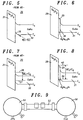
- FIG. 2 a simplified bandgap diagram of interface structure 10 is illustrated.
- the conduction band is designated E c and the valence band is designated E v .
- the bandgap of compound semiconductor substrate 11, which in this specific example is GaAs is illustrated as area 21 (hereinafter bandgap 21) at the right of the diagram.
- the bandgap of spacer layer 15 which is illustrated as area 25 (hereinafter bandgap 25) adjoins bandgap 21 of compound semiconductor substrate 11 at the left and is wider than bandgap 21.
- the bandgap of insulating layer 18, which in this specific example is Ga 2 O 3 is illustrated as area 28 (hereinafter bandgap 8) adjoins bandgap 25 of spacer layer 15 at the left and is wider than bandgap 25.
- Interface structure 10 of FIG. 1 has several advantages which can best be explained with reference to bandgap diagrams of prior art structures compared to the bandgap diagram of interface structure 10.
- a bandgap diagram is illustrated for a prior art interface 30 wherein an insulating layer of Ga 2 O 3 , represented by a bandgap 31, is deposited directly on the surface of a compound semiconductor material of GaAs, represented by a bandgap 32.
- the bandgap diagram of FIG. 3 is biased as it would be in normal operation and illustrates insulator trapping centers N t and the trapping of carriers therein.
- the trapping of carriers into insulator trapping centers N t occurs directly from the reservoir of inversion or accumulation carriers (n 2D >10 12 cm -2 ) located at the insulator-compound semiconductor interface.
- the density of carriers available for trapping is reduced by orders of magnitude.
- the tunneling probability which exponentially depends on ⁇ E (the band offset at the interface of compound semiconductor substrate 11 and spacer layer 15) and ⁇ x (the thickness of spacer layer 15), determines the density of carriers available for trapping processes.
- the density of carriers at the insulator-compound semiconductor interface is: N 1 ⁇ n 2D e - ⁇ E/kT
- FIGS. 5 and 6 are bandgap diagrams similar to FIGS. 3 and 4.
- a bandgap diagram is illustrated for prior art interface 30 wherein an insulating layer of Ga 2 O 3 , represented by bandgap 31, is deposited directly on the surface of a compound semiconductor material of GaAs, represented by a bandgap 32.
- the bandgap diagram of FIG. 5 is biased as it would be in normal operation and illustrates the substrate injection of hot carriers from the inversion/accumulation channel into the insulating layer (bandgap 31).
- the bandgap diagram of FIG. 6 represents the structure of FIG. 1 and the various bandgaps are numbered the same as in FIG. 4.
- a distribution curve N(E)F(E) in FIG. 5 indicates the distribution of carriers adjacent the interface of the compound semiconductor material and the insulating layer where carriers below dashed line 35 (quantum well ground state) can contribute.
- a distribution curve N(E)F(E) in FIG. 6 indicates the distribution of carriers adjacent the compound semiconductor substrate 11 and spacer layer 15 where only carriers below dashed line 36 can contribute.
- N(E), F(E), and E are the density of states, the Fermi-Dirac distribution function, and the energy, respectively.
- bandgap 28 the substrate injection of hot carriers into insulator layer 18
- the microroughness and defects inherent in a deposited layer are between insulating layer 18 and spacer layer 15, whereas the interface between spacer layer 15 and compound semiconductor layer 11 is smooth and defect free because spacer layer 15 is grown on the surface of compound semiconductor substrate 11.
- FIGS. 7 and 8 Another advantage of interface structure 10 is illustrated in FIGS. 7 and 8, in which bandgap diagrams similar to FIGS. 3 and 4, respectively, are illustrated and similar bandgaps are designated with similar numbers.
- FIG. 4 localized, stress induced interfacial states are located in bandgap 32 of the compound semiconductor in which the inversion/accumulation channel forms. That is, ⁇ E f ⁇ E G , as illustrated by lines 37 and 38, where ⁇ E f is the energy range of free Fermi level movement and EG is the bandgap between E c and E v .
- FIG. 10 Another advantage of interface structure 10 is illustrated in FIGS. 7 and 8, in which bandgap diagrams similar to FIGS. 3 and 4, respectively, are illustrated and similar bandgaps are designated with similar numbers.
- FIG. 4 localized, stress induced interfacial states are located in bandgap 32 of the compound semiconductor in which the inversion/accumulation channel forms. That is, ⁇ E f ⁇ E
- System 50 includes a transfer and load module 53, a III-V growth chamber 55 attached to transfer and load module 53, and an insulator chamber 58 attached to transfer and load module 53.
- Each of chambers 55 and 58 are attached to transfer and load module 53 so that wafers, chips, etc. can be processed in each chamber without removing the wafers from the system.
- a compound semiconductor substrate is placed in transfer and load module 53 and the pressure in multi-wafer production system 50 is reduced to ⁇ 1.33 x 10 -8 Pa (10 -10 Torr).
- the compound semiconductor substrate is then moved to III-V growth chamber 55 and a compound semiconductor epitaxial layer (e.g. material 11 of FIG. 1) and a spacer layer of compound semiconductor material (e.g. spacer layer 15 of FIG. 1) having a bandgap which is wider than the bandgap of compound semiconductor substrate 11 are epitaxially grown on the compound semiconductor substrate.
- compound semiconductor substrate 11 is moved to transfer and load module 53 and then to insulator chamber 58.
- insulator chamber 58 an insulating layer (e.g. insulating layer 18 of FIG. 1) is deposited on spacer layer 15.
- a new and improved insulator-compound semiconductor interface structure is disclosed along with novel methods of fabrication.
- the new and improved insulator-compound semiconductor interface structure has improved stability and reliability and is relatively easy to fabricate and use.
- the new and improved insulator-compound semiconductor interface structure can be formed in situ to further reduce impurities and to further simplify fabrication.
Landscapes
- Engineering & Computer Science (AREA)
- Physics & Mathematics (AREA)
- Condensed Matter Physics & Semiconductors (AREA)
- General Physics & Mathematics (AREA)
- Manufacturing & Machinery (AREA)
- Computer Hardware Design (AREA)
- Microelectronics & Electronic Packaging (AREA)
- Power Engineering (AREA)
- Insulated Gate Type Field-Effect Transistor (AREA)
- Recrystallisation Techniques (AREA)
- Formation Of Insulating Films (AREA)
- Junction Field-Effect Transistors (AREA)
Applications Claiming Priority (2)
| Application Number | Priority Date | Filing Date | Title |
|---|---|---|---|
| US08/812,952 US6359294B1 (en) | 1997-03-04 | 1997-03-04 | Insulator-compound semiconductor interface structure |
| US812952 | 1997-03-04 |
Publications (2)
| Publication Number | Publication Date |
|---|---|
| EP0863539A1 EP0863539A1 (en) | 1998-09-09 |
| EP0863539B1 true EP0863539B1 (en) | 2004-10-20 |
Family
ID=25211069
Family Applications (1)
| Application Number | Title | Priority Date | Filing Date |
|---|---|---|---|
| EP98103610A Expired - Lifetime EP0863539B1 (en) | 1997-03-04 | 1998-03-02 | Insulator-compound semiconductor interface-structure and methods of fabrication |
Country Status (4)
| Country | Link |
|---|---|
| US (1) | US6359294B1 (enExample) |
| EP (1) | EP0863539B1 (enExample) |
| JP (1) | JP3920447B2 (enExample) |
| DE (1) | DE69827058T2 (enExample) |
Families Citing this family (3)
| Publication number | Priority date | Publication date | Assignee | Title |
|---|---|---|---|---|
| KR20130092548A (ko) | 2010-08-31 | 2013-08-20 | 스미또모 가가꾸 가부시키가이샤 | 반도체 기판, 절연 게이트형 전계 효과 트랜지스터 및 반도체 기판의 제조 방법 |
| CN103098188B (zh) | 2010-08-31 | 2016-03-30 | 住友化学株式会社 | 半导体基板及绝缘栅极型场效电子晶体管 |
| CN106560928B (zh) * | 2015-09-28 | 2019-11-08 | 河北大学 | 一种电荷俘获型存储元件及其制备工艺 |
Family Cites Families (5)
| Publication number | Priority date | Publication date | Assignee | Title |
|---|---|---|---|---|
| US4859253A (en) * | 1988-07-20 | 1989-08-22 | International Business Machines Corporation | Method for passivating a compound semiconductor surface and device having improved semiconductor-insulator interface |
| US5124762A (en) * | 1990-12-31 | 1992-06-23 | Honeywell Inc. | Gaas heterostructure metal-insulator-semiconductor integrated circuit technology |
| US5334865A (en) * | 1991-07-31 | 1994-08-02 | Allied-Signal Inc. | MODFET structure for threshold control |
| US5597768A (en) * | 1996-03-21 | 1997-01-28 | Motorola, Inc. | Method of forming a Ga2 O3 dielectric layer |
| US5747838A (en) * | 1996-11-27 | 1998-05-05 | The Regents Of The University Of California | Ultra-low phase noise GaAs MOSFETs |
-
1997
- 1997-03-04 US US08/812,952 patent/US6359294B1/en not_active Expired - Lifetime
-
1998
- 1998-03-02 JP JP06780298A patent/JP3920447B2/ja not_active Expired - Lifetime
- 1998-03-02 EP EP98103610A patent/EP0863539B1/en not_active Expired - Lifetime
- 1998-03-02 DE DE69827058T patent/DE69827058T2/de not_active Expired - Fee Related
Also Published As
| Publication number | Publication date |
|---|---|
| DE69827058D1 (de) | 2004-11-25 |
| US6359294B1 (en) | 2002-03-19 |
| JP3920447B2 (ja) | 2007-05-30 |
| DE69827058T2 (de) | 2005-03-03 |
| JPH10275806A (ja) | 1998-10-13 |
| EP0863539A1 (en) | 1998-09-09 |
Similar Documents
| Publication | Publication Date | Title |
|---|---|---|
| US12034051B2 (en) | Nitride-based semiconductor device and method of manufacturing the same | |
| KR20000006005A (ko) | 비소화갈륨계반도체본체위에산화층을구비한아티클,및아티클의제조방법 | |
| US7187045B2 (en) | Junction field effect metal oxide compound semiconductor integrated transistor devices | |
| US6989556B2 (en) | Metal oxide compound semiconductor integrated transistor devices with a gate insulator structure | |
| US20070138506A1 (en) | Nitride metal oxide semiconductor integrated transistor devices | |
| KR102716586B1 (ko) | 채널 이동도를 증가시키기 위한 양자 컴퓨팅 디바이스의 제조 동안의 처리 | |
| EP0397148B1 (en) | Heterostructure device and production method thereof | |
| US4987095A (en) | Method of making unpinned oxide-compound semiconductor structures | |
| US5086321A (en) | Unpinned oxide-compound semiconductor structures and method of forming same | |
| EP0863539B1 (en) | Insulator-compound semiconductor interface-structure and methods of fabrication | |
| Okada et al. | Observation of Coulomb blockade type conductance oscillations up to 50 K in gated InGaAs ridge quantum wires grown by molecular beam epitaxy on InP substrates | |
| Nguyen et al. | Investigating FinFET sidewall passivation using epitaxial (100) Ge and (110) Ge metal–oxide–semiconductor devices on AlAs/GaAs | |
| KR20000011954A (ko) | 갈륨아세닉베이스반도체본체상에산화물층을포함하는제품제조방법 | |
| US5219772A (en) | Method for making field effect devices with ultra-short gates | |
| EP0517443B1 (en) | Method of fabricating GaAs mesfets with enhanced schottky barrier | |
| US6953729B2 (en) | Heterojunction field effect transistor and manufacturing method thereof | |
| EP1315852A1 (en) | Epitaxial wafer apparatus | |
| Maeda et al. | DC and RF characteristics in Al2O3/Si3N4 insulated-gate AlGaN/GaN heterostructure field-effect transistors | |
| JP2803555B2 (ja) | 極微細トンネル障壁の作製方法 | |
| Yamada et al. | Fabrication and characterization of novel oxide-free InP metal-insulator-semiconductor FETs having an ultra narrow Si surface quantum well | |
| KR0170189B1 (ko) | 격자비정합 고전자 이동도 트랜지스터 | |
| Kwo et al. | High κ Gate Dielectrics for Compound Semiconductors | |
| Gerard et al. | Monolithic Integration of III-V Microcavity Leds on Silicon Drivers using Conformal Epitaxy | |
| Kanber et al. | Optimization of selective area growth of GaAs by low pressure organometallic vapor phase epitaxy for monolithic integrated circuits | |
| Gucmann | GaAs-based MOS Structures |
Legal Events
| Date | Code | Title | Description |
|---|---|---|---|
| PUAI | Public reference made under article 153(3) epc to a published international application that has entered the european phase |
Free format text: ORIGINAL CODE: 0009012 |
|
| AK | Designated contracting states |
Kind code of ref document: A1 Designated state(s): DE FR GB |
|
| AX | Request for extension of the european patent |
Free format text: AL;LT;LV;MK;RO;SI |
|
| 17P | Request for examination filed |
Effective date: 19990309 |
|
| AKX | Designation fees paid |
Free format text: DE FR GB |
|
| RBV | Designated contracting states (corrected) |
Designated state(s): DE FR GB |
|
| 17Q | First examination report despatched |
Effective date: 20011017 |
|
| GRAP | Despatch of communication of intention to grant a patent |
Free format text: ORIGINAL CODE: EPIDOSNIGR1 |
|
| GRAS | Grant fee paid |
Free format text: ORIGINAL CODE: EPIDOSNIGR3 |
|
| GRAA | (expected) grant |
Free format text: ORIGINAL CODE: 0009210 |
|
| AK | Designated contracting states |
Kind code of ref document: B1 Designated state(s): DE FR GB |
|
| REG | Reference to a national code |
Ref country code: GB Ref legal event code: FG4D |
|
| REF | Corresponds to: |
Ref document number: 69827058 Country of ref document: DE Date of ref document: 20041125 Kind code of ref document: P |
|
| RAP2 | Party data changed (patent owner data changed or rights of a patent transferred) |
Owner name: FREESCALE SEMICONDUCTOR, INC. |
|
| PLBE | No opposition filed within time limit |
Free format text: ORIGINAL CODE: 0009261 |
|
| STAA | Information on the status of an ep patent application or granted ep patent |
Free format text: STATUS: NO OPPOSITION FILED WITHIN TIME LIMIT |
|
| ET | Fr: translation filed | ||
| 26N | No opposition filed |
Effective date: 20050721 |
|
| PGFP | Annual fee paid to national office [announced via postgrant information from national office to epo] |
Ref country code: GB Payment date: 20070202 Year of fee payment: 10 |
|
| PGFP | Annual fee paid to national office [announced via postgrant information from national office to epo] |
Ref country code: DE Payment date: 20070330 Year of fee payment: 10 |
|
| PGFP | Annual fee paid to national office [announced via postgrant information from national office to epo] |
Ref country code: FR Payment date: 20070301 Year of fee payment: 10 |
|
| GBPC | Gb: european patent ceased through non-payment of renewal fee |
Effective date: 20080302 |
|
| REG | Reference to a national code |
Ref country code: FR Ref legal event code: ST Effective date: 20081125 |
|
| PG25 | Lapsed in a contracting state [announced via postgrant information from national office to epo] |
Ref country code: DE Free format text: LAPSE BECAUSE OF NON-PAYMENT OF DUE FEES Effective date: 20081001 |
|
| PG25 | Lapsed in a contracting state [announced via postgrant information from national office to epo] |
Ref country code: FR Free format text: LAPSE BECAUSE OF NON-PAYMENT OF DUE FEES Effective date: 20080331 |
|
| PG25 | Lapsed in a contracting state [announced via postgrant information from national office to epo] |
Ref country code: GB Free format text: LAPSE BECAUSE OF NON-PAYMENT OF DUE FEES Effective date: 20080302 |