EP0861018A2 - Tiefdruckverfahren, Tiefdrucker, Verfahren zur Herstellung von Höckern oder Leitermustern, Vorrichtung dafür, Höckerelektrode und gedruckte Leiterplatte - Google Patents
Tiefdruckverfahren, Tiefdrucker, Verfahren zur Herstellung von Höckern oder Leitermustern, Vorrichtung dafür, Höckerelektrode und gedruckte Leiterplatte Download PDFInfo
- Publication number
- EP0861018A2 EP0861018A2 EP98103046A EP98103046A EP0861018A2 EP 0861018 A2 EP0861018 A2 EP 0861018A2 EP 98103046 A EP98103046 A EP 98103046A EP 98103046 A EP98103046 A EP 98103046A EP 0861018 A2 EP0861018 A2 EP 0861018A2
- Authority
- EP
- European Patent Office
- Prior art keywords
- paste
- fused metal
- printing master
- portions
- printing
- Prior art date
- Legal status (The legal status is an assumption and is not a legal conclusion. Google has not performed a legal analysis and makes no representation as to the accuracy of the status listed.)
- Granted
Links
Images


Classifications
-
- B—PERFORMING OPERATIONS; TRANSPORTING
- B41—PRINTING; LINING MACHINES; TYPEWRITERS; STAMPS
- B41M—PRINTING, DUPLICATING, MARKING, OR COPYING PROCESSES; COLOUR PRINTING
- B41M1/00—Inking and printing with a printer's forme
- B41M1/10—Intaglio printing ; Gravure printing
-
- H—ELECTRICITY
- H05—ELECTRIC TECHNIQUES NOT OTHERWISE PROVIDED FOR
- H05K—PRINTED CIRCUITS; CASINGS OR CONSTRUCTIONAL DETAILS OF ELECTRIC APPARATUS; MANUFACTURE OF ASSEMBLAGES OF ELECTRICAL COMPONENTS
- H05K3/00—Apparatus or processes for manufacturing printed circuits
- H05K3/10—Apparatus or processes for manufacturing printed circuits in which conductive material is applied to the insulating support in such a manner as to form the desired conductive pattern
- H05K3/20—Apparatus or processes for manufacturing printed circuits in which conductive material is applied to the insulating support in such a manner as to form the desired conductive pattern by affixing prefabricated conductor pattern
- H05K3/207—Apparatus or processes for manufacturing printed circuits in which conductive material is applied to the insulating support in such a manner as to form the desired conductive pattern by affixing prefabricated conductor pattern using a prefabricated paste pattern, ink pattern or powder pattern
-
- H—ELECTRICITY
- H05—ELECTRIC TECHNIQUES NOT OTHERWISE PROVIDED FOR
- H05K—PRINTED CIRCUITS; CASINGS OR CONSTRUCTIONAL DETAILS OF ELECTRIC APPARATUS; MANUFACTURE OF ASSEMBLAGES OF ELECTRICAL COMPONENTS
- H05K3/00—Apparatus or processes for manufacturing printed circuits
- H05K3/30—Assembling printed circuits with electric components, e.g. with resistors
- H05K3/32—Assembling printed circuits with electric components, e.g. with resistors electrically connecting electric components or wires to printed circuits
- H05K3/34—Assembling printed circuits with electric components, e.g. with resistors electrically connecting electric components or wires to printed circuits by soldering
- H05K3/3465—Application of solder
- H05K3/3468—Application of molten solder, e.g. dip soldering
-
- H—ELECTRICITY
- H05—ELECTRIC TECHNIQUES NOT OTHERWISE PROVIDED FOR
- H05K—PRINTED CIRCUITS; CASINGS OR CONSTRUCTIONAL DETAILS OF ELECTRIC APPARATUS; MANUFACTURE OF ASSEMBLAGES OF ELECTRICAL COMPONENTS
- H05K3/00—Apparatus or processes for manufacturing printed circuits
- H05K3/40—Forming printed elements for providing electric connections to or between printed circuits
- H05K3/4007—Surface contacts, e.g. bumps
-
- H—ELECTRICITY
- H10—SEMICONDUCTOR DEVICES; ELECTRIC SOLID-STATE DEVICES NOT OTHERWISE PROVIDED FOR
- H10W—GENERIC PACKAGES, INTERCONNECTIONS, CONNECTORS OR OTHER CONSTRUCTIONAL DETAILS OF DEVICES COVERED BY CLASS H10
- H10W70/00—Package substrates; Interposers; Redistribution layers [RDL]
- H10W70/01—Manufacture or treatment
- H10W70/05—Manufacture or treatment of insulating or insulated package substrates, or of interposers, or of redistribution layers
- H10W70/093—Connecting or disconnecting other interconnections thereto or therefrom, e.g. connecting bond wires or bumps
-
- H—ELECTRICITY
- H10—SEMICONDUCTOR DEVICES; ELECTRIC SOLID-STATE DEVICES NOT OTHERWISE PROVIDED FOR
- H10W—GENERIC PACKAGES, INTERCONNECTIONS, CONNECTORS OR OTHER CONSTRUCTIONAL DETAILS OF DEVICES COVERED BY CLASS H10
- H10W70/00—Package substrates; Interposers; Redistribution layers [RDL]
- H10W70/01—Manufacture or treatment
- H10W70/05—Manufacture or treatment of insulating or insulated package substrates, or of interposers, or of redistribution layers
- H10W70/098—Applying pastes or inks, e.g. screen printing
-
- H—ELECTRICITY
- H05—ELECTRIC TECHNIQUES NOT OTHERWISE PROVIDED FOR
- H05K—PRINTED CIRCUITS; CASINGS OR CONSTRUCTIONAL DETAILS OF ELECTRIC APPARATUS; MANUFACTURE OF ASSEMBLAGES OF ELECTRICAL COMPONENTS
- H05K2201/00—Indexing scheme relating to printed circuits covered by H05K1/00
- H05K2201/03—Conductive materials
- H05K2201/0332—Structure of the conductor
- H05K2201/0364—Conductor shape
- H05K2201/0367—Metallic bump or raised conductor not used as solder bump
-
- H—ELECTRICITY
- H05—ELECTRIC TECHNIQUES NOT OTHERWISE PROVIDED FOR
- H05K—PRINTED CIRCUITS; CASINGS OR CONSTRUCTIONAL DETAILS OF ELECTRIC APPARATUS; MANUFACTURE OF ASSEMBLAGES OF ELECTRICAL COMPONENTS
- H05K2203/00—Indexing scheme relating to apparatus or processes for manufacturing printed circuits covered by H05K3/00
- H05K2203/01—Tools for processing; Objects used during processing
- H05K2203/0104—Tools for processing; Objects used during processing for patterning or coating
- H05K2203/0113—Female die used for patterning or transferring, e.g. temporary substrate having recessed pattern
-
- H—ELECTRICITY
- H05—ELECTRIC TECHNIQUES NOT OTHERWISE PROVIDED FOR
- H05K—PRINTED CIRCUITS; CASINGS OR CONSTRUCTIONAL DETAILS OF ELECTRIC APPARATUS; MANUFACTURE OF ASSEMBLAGES OF ELECTRICAL COMPONENTS
- H05K2203/00—Indexing scheme relating to apparatus or processes for manufacturing printed circuits covered by H05K3/00
- H05K2203/03—Metal processing
- H05K2203/0338—Transferring metal or conductive material other than a circuit pattern, e.g. bump, solder, printed component
-
- H—ELECTRICITY
- H05—ELECTRIC TECHNIQUES NOT OTHERWISE PROVIDED FOR
- H05K—PRINTED CIRCUITS; CASINGS OR CONSTRUCTIONAL DETAILS OF ELECTRIC APPARATUS; MANUFACTURE OF ASSEMBLAGES OF ELECTRICAL COMPONENTS
- H05K2203/00—Indexing scheme relating to apparatus or processes for manufacturing printed circuits covered by H05K3/00
- H05K2203/07—Treatments involving liquids, e.g. plating, rinsing
- H05K2203/0736—Methods for applying liquids, e.g. spraying
- H05K2203/074—Features related to the fluid pressure
-
- H—ELECTRICITY
- H05—ELECTRIC TECHNIQUES NOT OTHERWISE PROVIDED FOR
- H05K—PRINTED CIRCUITS; CASINGS OR CONSTRUCTIONAL DETAILS OF ELECTRIC APPARATUS; MANUFACTURE OF ASSEMBLAGES OF ELECTRICAL COMPONENTS
- H05K2203/00—Indexing scheme relating to apparatus or processes for manufacturing printed circuits covered by H05K3/00
- H05K2203/08—Treatments involving gases
- H05K2203/085—Using vacuum or low pressure
-
- H—ELECTRICITY
- H05—ELECTRIC TECHNIQUES NOT OTHERWISE PROVIDED FOR
- H05K—PRINTED CIRCUITS; CASINGS OR CONSTRUCTIONAL DETAILS OF ELECTRIC APPARATUS; MANUFACTURE OF ASSEMBLAGES OF ELECTRICAL COMPONENTS
- H05K2203/00—Indexing scheme relating to apparatus or processes for manufacturing printed circuits covered by H05K3/00
- H05K2203/08—Treatments involving gases
- H05K2203/086—Using an inert gas
-
- H—ELECTRICITY
- H10—SEMICONDUCTOR DEVICES; ELECTRIC SOLID-STATE DEVICES NOT OTHERWISE PROVIDED FOR
- H10W—GENERIC PACKAGES, INTERCONNECTIONS, CONNECTORS OR OTHER CONSTRUCTIONAL DETAILS OF DEVICES COVERED BY CLASS H10
- H10W72/00—Interconnections or connectors in packages
- H10W72/01—Manufacture or treatment
- H10W72/011—Apparatus therefor
- H10W72/0112—Apparatus for manufacturing bump connectors
-
- H—ELECTRICITY
- H10—SEMICONDUCTOR DEVICES; ELECTRIC SOLID-STATE DEVICES NOT OTHERWISE PROVIDED FOR
- H10W—GENERIC PACKAGES, INTERCONNECTIONS, CONNECTORS OR OTHER CONSTRUCTIONAL DETAILS OF DEVICES COVERED BY CLASS H10
- H10W72/00—Interconnections or connectors in packages
- H10W72/071—Connecting or disconnecting
- H10W72/0711—Apparatus therefor
-
- H—ELECTRICITY
- H10—SEMICONDUCTOR DEVICES; ELECTRIC SOLID-STATE DEVICES NOT OTHERWISE PROVIDED FOR
- H10W—GENERIC PACKAGES, INTERCONNECTIONS, CONNECTORS OR OTHER CONSTRUCTIONAL DETAILS OF DEVICES COVERED BY CLASS H10
- H10W72/00—Interconnections or connectors in packages
- H10W72/071—Connecting or disconnecting
- H10W72/072—Connecting or disconnecting of bump connectors
- H10W72/07221—Aligning
- H10W72/07227—Aligning involving guiding structures, e.g. spacers or supporting members
-
- H—ELECTRICITY
- H10—SEMICONDUCTOR DEVICES; ELECTRIC SOLID-STATE DEVICES NOT OTHERWISE PROVIDED FOR
- H10W—GENERIC PACKAGES, INTERCONNECTIONS, CONNECTORS OR OTHER CONSTRUCTIONAL DETAILS OF DEVICES COVERED BY CLASS H10
- H10W72/00—Interconnections or connectors in packages
- H10W72/071—Connecting or disconnecting
- H10W72/072—Connecting or disconnecting of bump connectors
- H10W72/07231—Techniques
- H10W72/07236—Soldering or alloying
-
- H—ELECTRICITY
- H10—SEMICONDUCTOR DEVICES; ELECTRIC SOLID-STATE DEVICES NOT OTHERWISE PROVIDED FOR
- H10W—GENERIC PACKAGES, INTERCONNECTIONS, CONNECTORS OR OTHER CONSTRUCTIONAL DETAILS OF DEVICES COVERED BY CLASS H10
- H10W72/00—Interconnections or connectors in packages
- H10W72/20—Bump connectors, e.g. solder bumps or copper pillars; Dummy bumps; Thermal bumps
- H10W72/241—Dispositions, e.g. layouts
-
- H—ELECTRICITY
- H10—SEMICONDUCTOR DEVICES; ELECTRIC SOLID-STATE DEVICES NOT OTHERWISE PROVIDED FOR
- H10W—GENERIC PACKAGES, INTERCONNECTIONS, CONNECTORS OR OTHER CONSTRUCTIONAL DETAILS OF DEVICES COVERED BY CLASS H10
- H10W72/00—Interconnections or connectors in packages
- H10W72/20—Bump connectors, e.g. solder bumps or copper pillars; Dummy bumps; Thermal bumps
- H10W72/281—Auxiliary members
- H10W72/285—Alignment aids, e.g. alignment marks
-
- H—ELECTRICITY
- H10—SEMICONDUCTOR DEVICES; ELECTRIC SOLID-STATE DEVICES NOT OTHERWISE PROVIDED FOR
- H10W—GENERIC PACKAGES, INTERCONNECTIONS, CONNECTORS OR OTHER CONSTRUCTIONAL DETAILS OF DEVICES COVERED BY CLASS H10
- H10W80/00—Direct bonding of chips, wafers or substrates
- H10W80/161—Aligning
- H10W80/168—Aligning using guiding structures
-
- Y—GENERAL TAGGING OF NEW TECHNOLOGICAL DEVELOPMENTS; GENERAL TAGGING OF CROSS-SECTIONAL TECHNOLOGIES SPANNING OVER SEVERAL SECTIONS OF THE IPC; TECHNICAL SUBJECTS COVERED BY FORMER USPC CROSS-REFERENCE ART COLLECTIONS [XRACs] AND DIGESTS
- Y10—TECHNICAL SUBJECTS COVERED BY FORMER USPC
- Y10S—TECHNICAL SUBJECTS COVERED BY FORMER USPC CROSS-REFERENCE ART COLLECTIONS [XRACs] AND DIGESTS
- Y10S428/00—Stock material or miscellaneous articles
- Y10S428/901—Printed circuit
-
- Y—GENERAL TAGGING OF NEW TECHNOLOGICAL DEVELOPMENTS; GENERAL TAGGING OF CROSS-SECTIONAL TECHNOLOGIES SPANNING OVER SEVERAL SECTIONS OF THE IPC; TECHNICAL SUBJECTS COVERED BY FORMER USPC CROSS-REFERENCE ART COLLECTIONS [XRACs] AND DIGESTS
- Y10—TECHNICAL SUBJECTS COVERED BY FORMER USPC
- Y10T—TECHNICAL SUBJECTS COVERED BY FORMER US CLASSIFICATION
- Y10T29/00—Metal working
- Y10T29/49—Method of mechanical manufacture
- Y10T29/49002—Electrical device making
- Y10T29/49117—Conductor or circuit manufacturing
- Y10T29/49124—On flat or curved insulated base, e.g., printed circuit, etc.
- Y10T29/49155—Manufacturing circuit on or in base
Definitions
- the present invention relates to an intaglio printing method and an intaglio printer suitable for forming a wiring pattern and/or bumps such as bump electrodes on a print receiving material on which printing is to be performed, such as a substrate and a semiconductor package, using a paste or a fused metal.
- the present invention also relates to a method of forming the wiring pattern and the bumps such as bump electrodes on a printing substrate on which printing is to be performed, such as a substrate and a semiconductor package, using the intaglio printing method, a method for forming a wiring pattern, an apparatus for carrying out the method of forming the wiring pattern, the bump electrode and the wiring pattern.
- a method of performing printing using a stamp and an electroconductive paste there are conventionally known a method of performing printing using a stamp and an electroconductive paste; a method of masking a substrate with a stencil and spraying an electroconductive material over the masked substrate; a method of depicting a conductive pattern, using a syringe; a method of depositing an electroconductive material on the concave and convex portions of a substrate and polishing the electroconductive deposited convex portions to form a wiring pattern in the concave portions, and using the concave portion as the wiring pattern; a method of forming a wiring pattern by die-casting an electroconductive material onto concave portions of a substrate; a method of printing a wiring pattern on the surface of a substrate, using a catalyst, and causing a metal to separate therefrom; a method of printing a wiring pattern on a substrate by performing vacuum deposition of a metal on the substrate through a stencil; and a method of forming a wiring pattern by bringing a metal
- the element technologies for the above-mentioned conventional methods are composed of a patterning technology and a film formation technology.
- the patterning is performed by printing or photolithography
- the film formation is performed by laminating metal foils or plating.
- Representative examples thereof are subtractive method and additive method.
- the subtractive method which is also referred to as etched foil method, is carried out by performing patterning by etching.
- This method is currently used most.
- a copper foil laminated plate is first fabricated by laminating a copper foil having fine projections on a laminating surface thereof on a substrate such as a glass epoxy substrate with the application of high pressure thereto.
- the copper foil side of the copper foil laminated plate is subjected to photoresist coating.
- a photo film with a design of a wiring pattern is then superimposed on the photoresist coated side of the plate, exposed to light and then subjected to development, whereby a photoresist masking Pattern is formed on the copper foil laminated plate.
- the copper foil laminated plate with the photoresist masking pattern is then etched, whereby a wiring pattern is formed on the copper foil laminated plate.
- This method has the shortcomings that the above-mentioned steps including the art work of the photo film are complicated, high density is difficult to attain in comparison with the additive method which will be described in detail later, and the method is more or less lacking in patterning reliability. Furthermore, a photo-resist, a resist releasing agent, an etching agent and others are required as auxiliary materials for this method, so that this method has a further shortcoming that the production cost including the cost for treating waste fluids to be discarded is high.
- the above-mentioned additive method is also called plating method.
- an adhesive agent is applied to the surface of a substrate such as a substrate made of glass epoxy, and then a catalyst is applied thereto to improve the adhesiveness of a plating.
- a photoresist is coated thereon and a photo film is superimposed on the coated photoresist, and exposure and development are then performed, whereby a masking pattern is formed.
- Non-electrolytic copper plating is performed in the areas free of the masking, whereby a wiring pattern is formed.
- This method is superior to the subtractive method for attaining high density and reliability, but has the shortcomings that the process is complicated and the production cost is high.
- solder balls are joined to the circuit pads on the side of the package.
- a fused solder is added dropwise to an oil which is heated above the melting point of the solder, whereby fused solder particles, each of which is substantially in the shape of a true sphere, are formed, and the thus formed fused solder particles are cooled, washed and classified in accordance with the particle sizes thereof.
- the solder balls for the formation of the bump electrode are thus produced.
- the solder balls are moved onto the pad on the side of the package, using absorption nozzles, reflowed and joined.
- the solder balls are expensive, the height of bump electrodes varies in accordance with the variation of the diameter of each bump electrode, so that an open portion is formed in a joining portion when the bump electrodes are mounted on a substrate. Furthermore, the bump electrodes may fall off the pad on the package side due to imperfect fusing of the bump electrodes and the pad on the package side. Cracks are formed in a junction portion between the bump electrodes on the package side and the pad on the substrate side, or the bump electrodes are peeled off the pad, due to the stress caused by the difference in the coefficient of thermal expansion between the substrate and the package.
- solder balls by cutting a thread solder or a ribbon solder with a predetermined length and punching the cut solder into a cylindrical solder, and fusing the solder to form solder balls, or a method of using the punched cylindrical solder as it is and moving the solder onto a pad of a package and subjecting solder to reflow.
- These methods also have the same shortcomings as mentioned above for the same reasons as mentioned above, such as the formation of the open portion in the junction portion, falling off of the bumps, the formation of cracks in the junction portion between the bump on the package side and the pad on the substrate side, or the peeling of the bump on the package side off the pad on the substrate side.
- solder paste As the printing masks used in this method, there are a stencil mask and an intaglio printing mask, and as the solders for use in this method, there are a solder paste and a fused solder. With the combination of such printing masks and the solders, various methods have been proposed. In the method of performing printing using a solder paste, it is necessary to perform reflow after the printing.
- the diameter of the bump changes in accordance with the variation of the filling amount of the solder into the mask which depends upon the degree of scooping the solder by a squeegee, and also in accordance with the variation of the degree of the passing of the solder through the mask, so that these methods have the shortcoming that open portions may be formed in the junction portion.
- the bump electrodes will fall off the pad on the package side.
- cracks ace formed in a junction portion between the bump electrodes on the package side and the pad on the substrate side, or the bump electrodes are peeled off the pad, due to the stress caused by the difference in the coefficient of thermal expansion between the substrate and the package.
- the loss of holes in the mask may occur due to the missing of cavity holes in a photosensitive resin formed by photolithography when plating is performed in the course of the production of a metal mask (that is, an additive mask) which is currently mainly used. This hinders the formation of fine bumps.
- a method comprising the steps of masking the circumference of a pad with a thin film of a liquid resist and then forming a bump electrode with electrolytic plating.
- the plating tends to spread transversely, so that this method is not suitable for forming bump electrodes with multiple pins.
- a method comprising the steps of forming deep holes in a thick dry film by photolithography and performing electrolytic plating in the deep holes to secure the plating thickness for the bumps. This method has a shortcoming that the production cost is high.
- a method of forming bump electrodes, using a conventional wire bonding technology for internal bonding of semiconductor packages is also proposed.
- balls formed by discharging to a metal thin wire at a tip of a capillary are bonded to a pad as they are to form bump electrodes.
- This method features how to cut unnecessary wire portions.
- Any of the cutting methods has the problem that the height of the bumps cannot be made uniform.
- a method of leveling the height of the bumps by use of a holding jig or by polishing, and a method of making the balls more spherical by being fused under reflow have been proposed.
- these methods have the shortcomings that bumps cannot be formed at a time and the production efficiency thereof is low and it is difficult to prepare bump electrodes with multiple pins.
- the conventional methods have not yet sufficiently attained requests such as (a) the formation of bumps with high density, (b) high production reliability free of the formation of open portions in the junction, the falling off of bumps, the formation of cracks in the junction portion between the bumps on the package side and the pad on the substrate side, or the peeling of the bumps on the package side off the pad on the substrate side, (c) the formation of bumps with high productivity, and (d) the reduction of the cost for the formation of the bump electrodes.
- a second object of the present invention is to provide a printer capable of performing the above-mentioned printing method.
- a third object of the present invention is to provide a method capable of forming bumps such as bump electrodes, a wiring pattern, the bumps and the wiring pattern, or the bumps and/or the wiring pattern on a printing substrate on which printing is to be performed, such as a substrate and a semiconductor package, with excellent reliability, when actually mounting the bumps on the printing substrate, free of the formation of open portions in a junction portion between the bumps on a package side and a pad on the substrate side, the falling off of bumps, the formation of cracks in the junction portion, or the peeling of the bumps on the package side off the pad on the substrate side, with low cost and high productivity.
- a fourth object of the present invention is to provide a method of forming a wiring pattern on a front or back side of a printed circuit board and/or on a resist-coated substrate and forming a junction portion and/or a crossover portion of the wiring pattern.
- a fifth object of the present invention is to provide an apparatus for forming the bumps and/or the wiring pattern on a substrate.
- a sixth object of the present invention is to provide a bump electrode with excellent reliability, when actually mounting the electrode on the printing substrate, free of the formation of open portions in a junction portion between the bump electrode on a package side and a pad on the substrate side, the falling off of the bump electrode, the formation of cracks in the junction portion, or the peeling of the bump electrode on the package side off the pad on the substrate side.
- a seventh object of the present invention is to provide a printed circuit board.
- an intaglio printing method an intaglio printer, methods of forming bumps, a wiring pattern, the bumps and the wiring pattern, or the bumps and/or the wiring pattern on a printing substrate, a method of forming a wiring pattern on a front or back side of a printed circuit board and/or on a resist-coated substrate and forming a junction portion and/or a crossover portion of the wiring pattern, an apparatus forming bumps and/or the wiring pattern on a substrate, a bump electrode, and a printed circuit board as described in detail in the present specification.
- the intaglio printing method of the present invention comprises the steps of (a) bringing an intaglio printing master having portions depressed in a printing shape below the surface of the printing master, in which depressed portions a paste or a fused material is filled, into close contact with a print receiving material which can receive the paste or the fused metal, and (b) separating the intaglio printing master from the print receiving material to transfer the paste or the fused material to the print receiving material, wherein the intaglio printing method further comprises the steps of:
- a wiring pattern or bumps can be easily obtained by repeatedly filling the depressed portions in a printing shape with the paste or the fused metal. Furthermore, the materials employed in this intaglio printing method are inexpensive and the number of the kinds of the materials is small, so that wiring patterns and bumps such as bump electrodes can be formed on a substrate or on a semiconductor package at low cost with exceedingly high productivity.
- the intaglio printing master having the depressed portions is immersed in the paste or the fused metal to fill the depressed portions with the paste or the fused metal, and the shielding plate is brought into close and sliding contact with the surface of the printing master to remove therefrom the paste or the fused metal and to close the openings of the depressed portions in which the paste or the fused material is filled, with the shielding plate, whereby a constant amount of the paste or the fused metal is placed in the depressed portions.
- the upper level of the paste or the fused material filled in the depressed portions becomes equal to the level of the surface of the printing master, so that a proper amount of the paste or the fused metal is constantly filled in the depressed portions.
- the paste or the fused metal can be transferred to the print receiving material in an amount corresponding to the amount thereof filled in the depressed portions.
- the shielding plate has a flat and smooth surface and comes into close contact with the surface of the printing master, so that the leakage of the paste or the fused metal from the openings of the depressed portions can be securely prevented. Accordingly, the transfer of the paste or the fused metal to unnecessary portions on the print receiving material and the deformation of the printing shape of the transferred paste or fused metal can also be securely prevented.
- the intaglio printing master be placed in vacuum or in an atmosphere of reduced pressure prior to the step (1) of immersing the intaglio printing master having the depressed portions in the paste or the fused metal.
- the printing master in vacuum or in an atmosphere of reduced pressure prior to the above step (1), gases remaining in the depressed portions, if any, can be removed, and the paste or the fused metal can be completely filled in the depressed portions up to every corner and end portion of the depressed portions.
- gases present in the paste or the fused metal can be removed therefrom when the paste or the fused metal is placed in vacuum or under reduced pressure, so that the filling of the paste or the fused metal in the depressions can be performed sufficiently.
- the intaglio printing method of the present invention it is preferable that in the step (1) of immersing the intaglio printing master having the depressed portions in the paste or the fused metal, pressure be applied to the paste or the fused metal in order to completely fill the depressed portions with the paste or the fused metal up to every corner and end portion of the depressed portions.
- the intaglio printing method of the present invention is carried out, using a paste which contains a metal, or a fused metal, it is also preferable that the intaglio printing method be carried out in an atmosphere of an inert gas under reduced pressure in order to prevent the oxidation of the metal.
- the printing master be brought into close contact with the print receiving material, and then be separated from the print receiving material to transfer the paste or the fused metal filled in the depressed portions of the printing master to the print receiving material, while the paste in the depressed portions is in an unsolidified state, or while the fused metal in the depressed portions is still in a fused state, since by this process, the fused metal or the paste transferred to the print receiving material can be caused to firmly adhere to the print receiving material.
- the step (5) of bringing the printing master free of the shielding plate into close contact with the print receiving material, and the step (6) of separating the printing master from the print receiving material to transfer the paste or the fused metal in the printing shape to the print receiving material be carried out while the paste in the depressed portions is in an unsolidified state, or while the fused metal in the depressed portions is still in a fused state.
- the printing master be brought into close contact with the print receiving material, while the paste in the depressed portions is in an unsolidified state, or while the fused metal in the depressed portions is still in a fused state, and the paste or the fused metal filled in the depressed portions be solidified, for instance, by cooling, and then the printing master be separated from the print receiving material to transfer the paste or the metal solidified in the depressed portions of the printing master to the print receiving material, since by this process, the metal or the paste can be accurately transferred in the desired printing shape to the print receiving material, and the metal or the paste transferred to the print receiving material can be caused to firmly adhere to the print receiving material.
- the step (5) of bringing the printing master free of the shielding plate into close contact with the print receiving material be carried out while the paste in the depressed portions is in an unsolidified state, or while the fused metal in the depressed portions is still in a fused state
- the step (6) of separating the printing master from the print receiving material to transfer the paste or the fused metal in the printing shape to the print receiving material be carried out after the paste or the fused metal in the depressed portions is in a solidified state.
- the printing master to which the shielding plate is closely attached be taken out from the fused metal, and the fused metal in the depressed portions be cooled below the melting point of the fused metal, and then the shielding plate be separated from the surface of the printing mater, and the printing master free of the shielding plate be brought into close contact with the print receiving material, and then the cooled metal be heated to the melting point of the metal or above, and then cooled below the melting point of that metal, at that moment, the printing master be separated from the print receiving material to transfer the fused metal in the printing shape to the print receiving material.
- the fused metal in the depressed portions be cooled below the melting point of the fused metal, and the step (4) of separating the shielding plate from the surface of the printing mater be carried out, and in the step (5) of bringing the printing master free of the shielding plate into close contact with the print receiving material, the cooled metal in the depressed portions of the printing master be heated to the melting point of the metal or above, and then cooled below the melting point of the metal, at that moment, the printing master be separated from the print receiving material to transfer the fused metal in the printing shape to the print receiving material.
- the step (5) of bringing the printing master into close contact with the print receiving material be carried out with the printing master being in pressure contact with the print receiving material in any of the above-mentioned processes of the intaglio printing method of the present invention, in particular, while the fused metal in the depressed portions is still in a fused state or while the paste in the depressed portions is in an unsolidified state in order to fix the paste or the fused metal more firmly to the print receiving material.
- the intaglio printing master having portions depressed in the printing shape below the surface of the printing master for use in the present invention be made of a plastic material, more preferably an elastic plastic material.
- An intaglio printing master made of a plastic plate is less expensive than an intaglio printing master made of a metal.
- an elastic plastic material when used for the intaglio printing master, when the intaglio printing master with the depressed portions filled with the paste or the fused metal in the printing shape is brought into close and pressure contact with the print receiving material, the intaglio printing master can be brought into close contact with the surface of the printing master, so that the leakage of the paste or the fused metal from the openings of the depressed portions can be securely prevented. Accordingly, the transfer of the paste or the fused metal to unnecessary portions on the print receiving material and the deformation of the printing shape of the transferred paste or fused metal can also be securely prevented.
- depressed portions in the printing shape below the surface of the printing master by exima laser working because fine depressed portions in the printing shape with smooth inner walls, which are suitable for the formation of wiring patterns and/or bumps, can be formed by exima laser working.
- Representative examples of the paste for use in the intaglio printing method of the present invention are electroconductive adhesive agent, anisotropic electroconductive adhesive agent, electroconductive polymer, cream solder, tin paste, silver paste, silver palladium paste, and carbon paste.
- Representative examples of the fused metal for use in the intaglio printing method of the present invention are eutectic solder, high-temperature solder, low-temperature solider, tin, silver, and palladium.
- the intaglio printing method of the present invention can be easily carried out, for example, by an intaglio printer which is capable of (a) bringing an intaglio printing master having portions depressed in a printing shape below the surface of the printing master, in which depressed portions a paste or a fused metal is filled, into close contact with a print receiving material which can receive the paste or the fused metal, and (b) separating the intaglio printing master from the print receiving material to transfer the paste or the fused metal to the print receiving material,
- which intaglio printer comprises an airtight housing for holding therein the paste or the fused metal, provided with a vacant space therein, means for decreasing or increasing the pressure in the vacant space of the airtight housing, a shielding plate which can be brought into close and sliding contact with the surface of the printing master which is immersed in the paste or the fused metal to remove the paste or the fused metal therefrom and to close the openings of the depressed portions in which the paste or the fused metal is filled
- the shielding plate for use the above-mentioned intaglio printer, it is preferable that the surface of the shielding plate which comes into contact with the surface of the printing master be flat and smooth, and that the shielding plate be made of a plastic plate or sheet, such as a teflon plate or sheet, having a smooth surface, water repellency, wear-resistant properties, heat-resistant properties, and solvent-resistant properties.
- an intaglio printing master having bump female die portions and/or groove portions corresponding to the wiring pattern, each in a printing shape, depressed below the surface of the printing master, and the intaglio printing method of the present invention is carried out, which comprises the steps of (a) bringing the intaglio printing master, with a paste or a fused metal being filled in the bump female die portions and/or the groove portions, into close contact with a print receiving material, and (b) separating the intaglio printing master from the print receiving material to transfer the paste or the fused metal to the print receiving material, wherein the intaglio printing method further comprises the steps of:
- the intaglio printing master be placed in vacuum or in an atmosphere of reduced pressure prior to the step (1) of immersing the intaglio printing master having the bump female die portions and/or the groove portions, each in the printing shapes, in the paste or the fused metal to fill the bump female die portions and/or the groove portions with the paste or the fused metal
- the step (1) of immersing the intaglio printing master having the bump female die portions and/or the groove portions, each in the printing shapes, in the paste or the fused metal pressure be applied to the paste or the fused metal in order to completely fill the bump female die portions and/or the groove portions with the paste or the fused metal up to every corner and end portion of the depressed portions
- bumps there can be formed, on boards or substrates such as semiconductor packages, bumps such as bump electrodes with excellent reliability, free of the formation of open portions in a junction portion between the bumps on a package side and a pad on the substrate side, when actually mounting the bumps on the printing substrate, and also free of the falling off of bumps, the formation of cracks in the junction portion, or the peeling of the bumps on the package side off the pad on the substrate side, with low cost and high productivity.
- the bump female die portions in the shape of a circular cylinder, a cone or pyramid, or a frustum of a cone or pyramid can be easily formed in a plastic plate by exima laser working, whereby the above-mentioned excellent bumps can be formed.
- the depth and the width of the groove portions corresponding to the wiring pattern can be adjusted as desired, so that there can be easily formed a wiring pattern with a cross-section at right angles with respect to the extending direction of the corresponding groove portions having such an aspect ratio of the depth thereof to the width thereof that the depth thereof is greater than and the width thereof is smaller than the respective depth and width of an aspect ratio of 1 : 5, although it is difficult to form such a wiring pattern by conventional methods. Therefore, it is possible to reduce the width of the wiring pattern without reducing the cross-section of the wiring pattern, so that a wiring pattern with high density can be formed while maintaining the low resistance thereof.
- bumps and the wiring pattern can be formed on the substrate at the same time.
- the intaglio printing master having bump female die portions and/or groove portions corresponding to the wiring pattern, each in a printing shape, depressed below the surface of the printing master in the above-mentioned intaglio printing method, there can be formed bumps and/or a wiring pattern in a super-imposed manner on a printed circuit board which is fabricated by a conventional method.
- the wiring pattern fabricated by the method of the present invention can be formed on a wiring pattern of a printed circuit board fabricated by a conventional method and/on a resist coating provided on the conventional printed circuit board, thereby forming a junction portion of the wiring pattern on the conventional wiring pattern and the wiring pattern fabricated by the method of the present invention in a superimposed manner with direct contact between the two wiring patterns, and/or a crossover portion of the wiring pattern on the conventional wiring pattern and the wiring pattern fabricated by the method of the present invention, with the resist coating being interposed therebetween, but in a superimposed manner without direct contact between the two wiring patterns.
- the above-mentioned crossover portion and the above-mentioned junction portion can be selectively formed without difficulty, and therefore a printed circuit with complicated wiring patterns can be produced easily at low cost.
- the above-mentioned bumps and/or the wiring pattern can be easily formed on a substrate, for instance, by an apparatus, which is capable of (a) bringing an intaglio printing master having bump female die portions and/or groove portions corresponding to the wiring pattern, each in a printing shape, depressed below the surface of the printing master, in which bump female die portions and/or the groove portions a paste or a fused metal is filled, into close contact with a print receiving material, and (b) separating the intaglio printing master from the print receiving material to transfer the paste or the fused metal in the printing shape to the print receiving material, comprising:
- the wiring pattern can also be formed on a front or back side of a printed circuit board and/or on a resist-coated substrate with the formation of a junction portion and/or a crossover portion in the wiring pattern, using an intaglio printing master having groove portions depressed below the surface of the printing master, in a printing shape corresponding to the wiring pattern, by the intaglio printing method of the present invention.
- a bump electrode formed by the method of the present invention comprises a bump made from a fused metal in the shape of a circular cylinder, a cone or pyramide or a frustum of a cone or pyramid, formed on a substrate.
- a printed circuit board fabricated by using the above-mentioned method of the present invention comprises a substrate and a wiring pattern provided thereon which is made from a paste or a fused metal, having a cross-section at right angles with respect to the extending direction of said wiring pattern with such an aspect ratio of the depth thereof to the width thereof that the depth thereof is greater than and the width thereof is smaller than the respective depth and width of an aspect ratio of 1 : 5.
- Another printed circuit board fabricated by using the above-mentioned method of the present invention comprises a printed circuit substrate, a first wiring pattern and/or a resist coating formed on a front side or a back side of the printed circuit substrate, and a second wiring pattern made from a paste or a fused metal, which is formed on the first wiring pattern and/or the resist coating, thereby forming a junction portion of the first wiring pattern and the second wiring pattern and/or a crossover portion of the first wiring pattern and the second wiring pattern with the resist coating interposed therebetween.
- the second wiring pattern which is made from a paste or a fused metal may have a cross-section at right angles with respect to the extending direction of the wiring pattern with such an aspect ratio of the thickness thereof to the width thereof that the thickness thereof is greater than and the width thereof is smaller than the respective thickness and width of an aspect ratio of 1 : 5.
- the intaglio printing method of the present invention may comprises the steps of (a) bringing an intaglio printing master having portions depressed in a printing shape below the surface of the printing master, in which depressed portions a paste or a fused metal is filled, into close contact with a print receiving material, and (b) separating the intaglio printing master from the print receiving material to transfer the paste or the fused metal in the printing shape to the print receiving material, it is preferable that the intaglio printing master having the depressed portions be made of a plastic material.
- the plastic material be elastic.
- the intaglio printer of the present invention which is capable of (a) bringing an intaglio printing master having portions depressed in a printing shape below the surface of the printing master, in which depressed portions a paste or a fused metal is filled, into close contact with a print receiving material, and (b) separating the intaglio printing master from the print receiving material to transfer the paste or the fused metal to the print receiving material, it is preferable that the intaglio printing master having the depressed portions be made of a plastic material.
- the plastic material be elastic.
- FIG. 1 is a schematic cross-sectional view of an apparatus in explanation of the intaglio printing method of the present invention.
- FIG. 1 below an airtight housing 1, there is disposed a fused metal container 2 in which a fused metal 3, such as a eutectic solider or a high-temperature solider, serving as a material for a wiring pattern or a bump electrode, is held at a temperature of the melting point of the fused metal or above.
- a fused metal 3 such as a eutectic solider or a high-temperature solider, serving as a material for a wiring pattern or a bump electrode, is held at a temperature of the melting point of the fused metal or above.
- an inert gas 4 such as nitrogen gas for preventing the oxidation of the fused metal 3 is filled.
- Step A in FIG. 1 an intaglio printing master 5 made of a plastic material with slight elasticity, having depressed portions 6 in a printing shape, is placed in the inert gas 4 within the airtight housing 1.
- gases remaining in the depressed portions 6 are removed therefrom.
- the thus deaerated intaglio printing master 5 is then immersed in the fused metal 3.
- the pressure of the inert gas 4 is increased by the pressure increasing and decreasing apparatus 7, whereby pressure is applied to the fused metal 3, so that the fused metal 3 is completely filled in the depressed portions 6 without remaining any unfilled space in the depressed portions 6.
- Step B after the complete filling of the fused metal 3 in the depressed portions 6, a shielding plate 8 having a flat surface is brought into close and sliding contact with the surface of the printing master 5 in such a manner that the flat surface of the shielding plate 8 comes into contact with the surface of the printing master 5 on the side of the openings of the depressed portions 6 of the printing master 5, thereby removing the fused metal 3 staying on the surface of the printing master 5 therefrom, closing the openings of the depressed portions 6 of the printing master 5 with the shielding plate 8, whereby the fused metal 3 is completely removed from between the surface of the printing master 5 and the shielding plate 8, and a constant amount of the fused metal 3 is always filled in the depressed portions 6.
- Step C the printing master 5 with the fused metal being filled in the depressed portions 6 is taken out from the fused metal 3, together with the shielding plate 8 which is closely attached to the printing master 5, and then the printing master 5 is horizontally positioned in such a posture that the depressed portions 6 thereof come upward as illustrated.
- the shielding plate 8 is then slid in the direction of the arrow so as to remove the shielding plate 8 from the printing master 5.
- Step D a print receiving material 10 such as a package which is preheated for easing heat shock, with the printing side thereof being directed downward, is brought into close contact with the printing master 5 at a predetermined position, and the print receiving material 10 which is in close contact with the printing master 5 is turned upside-down. Sight pressure is applied to the printing master 5 and the print receiving material 10 by a pressure application apparatus 11. Due to the elasticity of the printing master 5 made of a plastic material, the fused metal 3 filled in the depressed portions 6 of the printing master 5 is securely brought into close contact with the print receiving material 10.
- Step E the printing master 5 and the print receiving material 10 are gradually cooled, and the fused metal 3 in the depressed portions 6 is solidified.
- the printing master 5 is then separated from the print receiving material 10, whereby the fused metal 8 filled in the depressed portions of the printing master 5 is transferred in the printing shape corresponding to the shape of the depressed portions 6 to the print receiving material 10 such as a package.
- bumps for BGA and CSF packages, and connection bumps of flip chip can be produced at low cost and with high uniformity.
- the depressed portions 6 of the printing master 5 can be formed by various methods such as mechanical working, photolithography, or plating.
- these methods have the shortcomings that the finer the bumps and the wiring patter, the more difficult the production, and the higher the production cost.
- These problems can be solved by forming the depressed portions in the printing shape in a plastic plate, using exima laser, since fine and small bump female die portions and grooves corresponding to a fine wiring pattern in a printing shape, depressed below the surface of the plastic plate, can be precisely formed by exima laser engraving work.
- FIG. 2a and FIG. 2b are schematic diagrams in explanation of an example of the formation of depressed portions in an intaglio printing master, using exima laser.
- a laser beam 13 emitted from an exima laser generator 12 is corrected with respect to the traveling direction and the aberration of the optical axis thereof by a miller 14 placed in the optical path of the laser beam 13, and then subjected to form adjustment by an optical shielding plate 15 for pattern setting, and patterned to form a patterned exima laser beam 16.
- the exima laser beam 16 is then condensed so as to have a necessary energy density, and projected to the surface of a plastic plate 21 which is to be used as an intaglio printing master, whereby abrasion working is carried out on the plastic plate 21.
- a worked hole 22 with a small tapering is formed by an exima laser beam 19 which is condensed so as to have a high energy density by an image lens 17 with a large condensation ratio
- a worked hole 23 with a large tapering is formed by an exima laser beam 20 which is condensed so as to have a low energy density by an image lens 18 with a small condensation ratio.
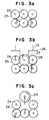
- FIG. 3a to FIG. 3c are schematic diagrams in explanation of the abrasion working by exima laser.
- a polymeric material such as a plastic material is composed of atoms 24 with the formation of covalent bonds therebetween with the electron orbitals 25 of the atoms overlapping sharing electrons so as to have a high energy density in the electron orbitals 25 to form a solid matter.
- the exima laser used in general in such molecular level abrasion working is a short wavelength ultraviolet light of exima laser with a wavelength of 248 nm for KrF gas, or with a wavelength of 193 nm for ArF gas. Because of the high resolution of the lihgt, extremely fine abrasion working can be carried out.
- the exima laser is a short pulse light, so that the engraving amount is proportional to the number of the pulses applied, and therefore it is possible to form a depressed portion with a predetermined depth in the plastic plate as desired by adjusting the number of the pulses applied thereto without making a through-hole in the plastic plate.
- the inner side walls of the engraved depressed portion reflect the exima laser beam and the absorption energy of the exima laser beam is attenuated, so that the angle of the side wall of the depressed portion at which an abrasion threshold limit value cannot be not exceeded becomes a working taper.
- the setting of the taper angle of the side wall of the depressed porting can be controlled or adjusted by changing the condensation ratio of the image lens with the replacement of the image lens, increasing or decreasing the output of the laser generator by changing the charging potential thereof, or by adjusting the attenuation ratio of the laser beam by an optical attenuator disposed in the optical path thereto.
- the top angle of a cone formed by the exima laser can be set as desired, and a conical depressed portion can be formed in the printing shape as desired, regardless of the top angle thereof, with an obtuse angle top or an acute angle top.
- a depressed portion 30 in the shape of a circular cylinder, a depressed portion 31 in the shape of a cone, and a depressed portion 32 in the shape of a frustum of a cone can be easily formed.
- depressed portions with a circular horizontal cross-section but also depressed portions with a quadrangular horizontal cross-section, for instance, a depressed portion 33 in the shape of a quadrangular prism, a depressed portion 34 in the shape of a quadrangular pyramid, and a depressed portion 35 in the shape of a frustum of a quadrangular pyramid can be easily formed by exima laser working, by using the light shielding plate 26 with the opening in the shape corresponding to the above-mentioned respective shape.
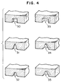
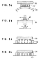
- stud bumps 42 for holding the package at the time of reflow and preventing the dropping of the package, and conical bumps 37 are used in combination, whereby pillar-shaped bumps 43 can be realized as shown in FIG. 6b.
- the junction of the pillar-shaped bumps which is difficult to achieve by the conventional method, can be easily achieved, so that the stress between the substrate and the package as in BGA, CSP and in the bump type junctions as flip chips can be reduced, and the occurrence of cracks in the junction cna be prevented, with the achievement of high reliability.
- the printing master 5 with the depressed portions 6 thereof being in the form of grooves corresponding to a wiring pattern to be formed on a printed circuit board such as a printing wiring board (PWB), the wiring pattern can be formed on the printed circuit board.
- PWB printing wiring board
- vibrations using ultrasonic wave, may be applied to the intaglio printing master 5 which is in close contact with the surface of the substrate, with the fused metal in the depressed portions in the form of grooves being brought into pressure contact with the surface of the substrate, whereby the fixing of the fused metal to the substrate can be enhanced.
- the shielding plate 8 for making constant the amount of the fused metal 3 filled in the depressed portions conta corresponding to the wiring pattern comes into contact with the fused metal 3 in the openings of the depressed portions to remove excess fused metal 3 therefrom, there is the risk that the fused metal 3 itself is separated into countless particles by the surface tension of the fused metal 3 and the wiring pattern to be continuously formed becomes discontinuous.
- the shielding plate 8 is removed from the surface of the printing master 5 after the fused metal 3 is cooled and solidified.
- the printing master 5 is brought into close contact with the substrate for PWB and then heated again to fuse the solidified metal and then cooled with the application of slight pressure thereto by the pressure application apparatus 11.
- the fused metal 3 is solidified, the printing master 5 is separated from the substrate, whereby a fine wiring pattern can be formed precisely and easily.
- the width and the depth of the grooves can be changed as desired and also the aspect ratio of the thickness and the width of the wiring pattern can also be easily changed as desired.
- the standard thickness of a copper foil used in the upper most surface portion of printed circuit boards is 18 ⁇ m.
- the width of the wiring pattern is still about 100 ⁇ m, so that the aspect ratio of the thickness to the width of the cross-section of the wiring pattern is about 1 : 5, which indicates that the wiring pattern is in a thin and broad shape.
- the cross-section of the wiring pattern can be change and adjusted by changing the shape of the grooves, so that it is possible to change the thickness of the cross-section of the wiring pattern so as to be greater than that of the aspect ratio of 1 : 5.
- the width of the wiring pattern can be reduced without changing the cross-section of the wiring pattern by the present invention, so that it is possible to form a wiring pattern with high density while maintaining the low resistance thereof.
- the bumps and/or the wiring pattern can be easily obtained by repeatedly filling the depressed portions in a printing shape with the paste or the fused metal, and exceedingly higher productivity can be attained in comparison with other production methods.
- the materials for the bumps and the wiring pattern for use in this method are inexpensive. It is also possible that ingots or line materials for automatic feeding can be used as they are as the materials for the bumps and the wiring pattern.
- auxiliary materials no materials other than inexpensive gas such as nitrogen and a mask cleaning agent for the intaglio printing master are necessary, so that bumps and the wiring pattern can be formed on boards and substrates such as semiconductor package at low cost.
- the above-mentioned method of forming the bumps and/or the wiring pattern can be carried out by using a simple apparatus, so that for example, the formation of bumps on the packages can be carried out in actual assembly lines, and while the heat at the formation of the bumps is still high, the mounting and the passage through a reflow furnace of the package can be performed, whereby the number of heat shocks, which is a conventional problem when guaranteeing the quality of the package, can be significantly reduced.
- pastes are electroconductive adhesive agent, anisotropic electroconductive adhesive agent, electroconductive polymer, cream solder, tin paste, silver paste, silver palladium paste, and carbon paste.
- electroconductive adhesive agent, anisotropic electroconductive adhesive agent, electroconductive polymer, and carbon paste it is unnecessary to fuse such pastes, and therefore heating and cooling of the pastes to be performed after the fusing are unnecessary. It is only necessary to separate the intaglio printing master from the boards or packages after the hardening of the paste.
- any of these is filled in the depressed portions of the intaglio printing master at room temperature, and the intaglio printing master is brought into close contact with a substrate, and is subjected to reflow with the intaglio printing master being in contact with the substrate to fuse the paste.
- the fused paste is then cooled and solidified, and then the intaglio printing master is separated from the substrate.
- the package or the substrate is usually placed with the print receiving side thereof up, and the intaglio printing master is overlaid thereon with the openings of the depressed portions of the printing master down, in close contact with the print receiving side of the substrate or the package, followed by the reflow.
- the heating, fusing, cooling and solidification be conducted, with the package as a print receiving material 10 and the intaglio printing master being situated in a slanting position in the longitudinal direction of the bumps as shown in FIG. 7.
- the pastes which require the fusing contain a flux in an amount of about 50%, so that the fused metal cannot occupy the entire space of the depressed portions of the intaglio printing master 5. Therefore, when the bumps are formed with the top end portions being directed upward, the upper end portion of the depressed portions 6 is filled with a flux with a smaller specific gravity, so that bumps without the top end portions are formed.
- a lacking portion 44 at the top end can be moved to one side of the conical bumps, so that the shape of the pillar-shaped bumps after the reflow is substantially the same as the shape of the pillar-shaped bumps after the reflow which can be achieved by the conical bump shape, and the effect of reducing the stress can be maintained.
- the lacking portion 44 on the side of the conical bump can be avoided to some extent by modifying the bump female die portion so as to expand toward the upper portion thereof as shown in FIG. 8, in such a shape of a bump lacking auxiliary filling shape 45.
Landscapes
- Engineering & Computer Science (AREA)
- Manufacturing & Machinery (AREA)
- Microelectronics & Electronic Packaging (AREA)
- Manufacturing Of Printed Wiring (AREA)
- Printing Methods (AREA)
- Manufacture Or Reproduction Of Printing Formes (AREA)
Applications Claiming Priority (3)
| Application Number | Priority Date | Filing Date | Title |
|---|---|---|---|
| JP5394897 | 1997-02-21 | ||
| JP53948/97 | 1997-02-21 | ||
| JP5394897 | 1997-02-21 |
Publications (3)
| Publication Number | Publication Date |
|---|---|
| EP0861018A2 true EP0861018A2 (de) | 1998-08-26 |
| EP0861018A3 EP0861018A3 (de) | 1999-07-14 |
| EP0861018B1 EP0861018B1 (de) | 2002-12-18 |
Family
ID=12956953
Family Applications (1)
| Application Number | Title | Priority Date | Filing Date |
|---|---|---|---|
| EP98103046A Expired - Lifetime EP0861018B1 (de) | 1997-02-21 | 1998-02-20 | Tiefdruckverfahren, Tiefdrucker, Verfahren zur Herstellung von Höckern oder Leitermustern, Vorrichtung dafür, Höckerelektrode und gedruckte Leiterplatte |
Country Status (6)
| Country | Link |
|---|---|
| US (2) | US6109175A (de) |
| EP (1) | EP0861018B1 (de) |
| KR (1) | KR19980071549A (de) |
| AT (1) | ATE230201T1 (de) |
| DE (1) | DE69810170D1 (de) |
| TW (1) | TW340296B (de) |
Cited By (5)
| Publication number | Priority date | Publication date | Assignee | Title |
|---|---|---|---|---|
| EP1162654A1 (de) * | 2000-06-06 | 2001-12-12 | I-Ming Chen | Verfahren zum Montieren eines Halbleiterchips auf einem Substrat und Halbleitervorrichtung geeignet für das Montieren auf einem Substrat |
| EP0932193A3 (de) * | 1998-01-22 | 2002-06-19 | Ricoh Microelectronics Co., Ltd. | Methode zur Herstellung von Höckerelektroden |
| DE10159539A1 (de) * | 2001-12-05 | 2003-06-26 | Hueck Folien Gmbh & Co Kg | Verfahren zur Herstellung eines Druckwerkzeugs, Druckwerkzeug und dessen Verwendung zum Verdrucken von insbesondere hochviskosen und/oder hochpigmentierten Lacken und Farben |
| FR2966008A1 (fr) * | 2010-10-12 | 2012-04-13 | Jean Noel Claveau | Procede de formation d’un circuit electrique par sublimation d’encre chargee de nanoparticules conductrice. |
| CN114521057A (zh) * | 2020-11-18 | 2022-05-20 | 深南电路股份有限公司 | 一种印制线路板及其制备方法 |
Families Citing this family (39)
| Publication number | Priority date | Publication date | Assignee | Title |
|---|---|---|---|---|
| TW374287B (en) | 1997-02-21 | 1999-11-11 | Ricoh Microelectronics Co Ltd | Gravure printing method and the device as well as the contact plate |
| US6316100B1 (en) | 1997-02-24 | 2001-11-13 | Superior Micropowders Llc | Nickel powders, methods for producing powders and devices fabricated from same |
| US7007833B2 (en) | 1997-05-27 | 2006-03-07 | Mackay John | Forming solder balls on substrates |
| US7842599B2 (en) * | 1997-05-27 | 2010-11-30 | Wstp, Llc | Bumping electronic components using transfer substrates |
| US7819301B2 (en) | 1997-05-27 | 2010-10-26 | Wstp, Llc | Bumping electronic components using transfer substrates |
| US6293456B1 (en) * | 1997-05-27 | 2001-09-25 | Spheretek, Llc | Methods for forming solder balls on substrates |
| US7654432B2 (en) | 1997-05-27 | 2010-02-02 | Wstp, Llc | Forming solder balls on substrates |
| US6609652B2 (en) | 1997-05-27 | 2003-08-26 | Spheretek, Llc | Ball bumping substrates, particuarly wafers |
| US7288471B2 (en) * | 1997-05-27 | 2007-10-30 | Mackay John | Bumping electronic components using transfer substrates |
| JPH11312711A (ja) * | 1998-04-30 | 1999-11-09 | Murata Mfg Co Ltd | 電子部品の接続方法 |
| TW409490B (en) * | 1998-12-31 | 2000-10-21 | World Wiser Electronics Inc | The equipment for plug hole process and the method thereof |
| KR100338329B1 (ko) * | 2000-02-25 | 2002-05-27 | 백승준 | 반도체 소자의 금속 배선 형성 방법 |
| US6354213B1 (en) * | 2000-04-03 | 2002-03-12 | Jerome D. Jenkins | Method and apparatus for cleaning a metering roll of a printing press |
| US6676991B2 (en) * | 2001-10-29 | 2004-01-13 | Hewlett-Packard Development Company, L.P. | Etch resist using printer technology |
| US6586843B2 (en) * | 2001-11-08 | 2003-07-01 | Intel Corporation | Integrated circuit device with covalently bonded connection structure |
| US6897089B1 (en) * | 2002-05-17 | 2005-05-24 | Micron Technology, Inc. | Method and system for fabricating semiconductor components using wafer level contact printing |
| US7082876B2 (en) * | 2002-06-07 | 2006-08-01 | Obducat Ab | Method for transferring a pattern |
| US6981318B2 (en) * | 2002-10-22 | 2006-01-03 | Jetta Company Limited | Printed circuit board manufacturing method |
| EP1569503B1 (de) * | 2002-12-06 | 2010-11-24 | Tamura Corporation | Verfahren zum zuführen von lot |
| WO2006076606A2 (en) | 2005-01-14 | 2006-07-20 | Cabot Corporation | Optimized multi-layer printing of electronics and displays |
| WO2006076608A2 (en) | 2005-01-14 | 2006-07-20 | Cabot Corporation | A system and process for manufacturing custom electronics by combining traditional electronics with printable electronics |
| WO2006076612A2 (en) | 2005-01-14 | 2006-07-20 | Cabot Corporation | A process for manufacturing application specific printable circuits (aspc’s) and other custom electronic devices |
| US7824466B2 (en) | 2005-01-14 | 2010-11-02 | Cabot Corporation | Production of metal nanoparticles |
| US8167393B2 (en) | 2005-01-14 | 2012-05-01 | Cabot Corporation | Printable electronic features on non-uniform substrate and processes for making same |
| US8383014B2 (en) | 2010-06-15 | 2013-02-26 | Cabot Corporation | Metal nanoparticle compositions |
| WO2006112384A1 (ja) * | 2005-04-15 | 2006-10-26 | Matsushita Electric Industrial Co., Ltd. | 電子部品接続用突起電極とそれを用いた電子部品実装体およびそれらの製造方法 |
| JP4637781B2 (ja) * | 2006-03-31 | 2011-02-23 | 昭和電工株式会社 | GaN系半導体発光素子の製造方法 |
| KR100746361B1 (ko) * | 2006-07-11 | 2007-08-06 | 삼성전기주식회사 | 인쇄회로기판 제조방법 |
| KR100792525B1 (ko) * | 2006-08-11 | 2008-01-09 | 삼성전기주식회사 | 인쇄회로기판 제조방법 |
| JP4961897B2 (ja) * | 2006-08-29 | 2012-06-27 | ソニー株式会社 | レーザー照射装置、レーザー照射方法、薄膜半導体装置の製造方法、及び表示装置の製造方法 |
| JP2008244361A (ja) * | 2007-03-28 | 2008-10-09 | Hitachi Via Mechanics Ltd | プリント基板のレーザ加工方法 |
| KR100866577B1 (ko) * | 2007-09-28 | 2008-11-03 | 삼성전기주식회사 | 인쇄회로기판의 층간 도통방법 |
| US8298611B2 (en) * | 2008-07-23 | 2012-10-30 | Seagate Technology Llc | Discrete track media |
| US20100031501A1 (en) * | 2008-08-08 | 2010-02-11 | Napra Co., Ltd. | Method for filling through hole or non-through hole formed on board with filler |
| US8534533B2 (en) * | 2012-01-19 | 2013-09-17 | Raytheon Company | Solder paste transfer process |
| US8770462B2 (en) | 2012-03-14 | 2014-07-08 | Raytheon Company | Solder paste transfer process |
| JP2015159277A (ja) * | 2014-01-23 | 2015-09-03 | パナソニック株式会社 | 電子デバイスの製造方法 |
| US11802337B1 (en) * | 2014-01-28 | 2023-10-31 | United States of America as Administrator of NASA | Atmospheric pressure plasma based fabrication process of printable electronics and functional coatings |
| TWI805953B (zh) * | 2020-10-15 | 2023-06-21 | 日商小森公司 | 球搭載方法及球搭載裝置 |
Family Cites Families (21)
| Publication number | Priority date | Publication date | Assignee | Title |
|---|---|---|---|---|
| US3560256A (en) * | 1966-10-06 | 1971-02-02 | Western Electric Co | Combined thick and thin film circuits |
| US4000054A (en) * | 1970-11-06 | 1976-12-28 | Microsystems International Limited | Method of making thin film crossover structure |
| AT337292B (de) * | 1971-09-02 | 1977-06-27 | Siemens Ag | Verfahren zur herstellung einer leiterplatte |
| US3806629A (en) * | 1972-07-03 | 1974-04-23 | Spacetac Inc | Crossover junction |
| US3821611A (en) * | 1973-09-21 | 1974-06-28 | Du Pont | Cross conductors with double layered insulation |
| US4417393A (en) * | 1981-04-01 | 1983-11-29 | General Electric Company | Method of fabricating high density electronic circuits having very narrow conductors |
| US4566384A (en) * | 1983-01-18 | 1986-01-28 | Dainippon Screen Mfg. Co., Ltd. | Intaglio printing plate and printing method |
| DE3433045A1 (de) * | 1984-09-08 | 1986-03-20 | Basf Ag, 6700 Ludwigshafen | Lichthaertbare verschlussmasse, insbesondere zum verschliessen des spaltes zwischen den enden von auf formzylinder aufgespannten tiefdruckplatten |
| GB2177262B (en) * | 1985-06-28 | 1988-08-10 | Gen Electric Co Plc | Electrical circuits |
| US4908346A (en) * | 1987-07-01 | 1990-03-13 | Eastman Kodak Company | Crystalline rare earth alkaline earth copper oxide thick film circuit element with superconducting onset transition temperature in excess of 77% |
| US5227223A (en) * | 1989-12-21 | 1993-07-13 | Monsanto Company | Fabricating metal articles from printed images |
| EP0452118B1 (de) * | 1990-04-12 | 1996-08-21 | Matsushita Electric Industrial Co., Ltd. | Leitende Tintenzusammensetzung und Verfahren zum Herstellen eines dickschichtigen Musters |
| US5362513A (en) * | 1990-05-10 | 1994-11-08 | Matsushita Electric Industrial Co., Ltd. | Method of manufacturing a pattern of conductive fine-line films and setting ink used for the same |
| JPH0467509A (ja) * | 1990-07-06 | 1992-03-03 | Kao Corp | 導電性ペースト及び導電性塗膜 |
| US5334804A (en) * | 1992-11-17 | 1994-08-02 | Fujitsu Limited | Wire interconnect structures for connecting an integrated circuit to a substrate |
| US5600103A (en) * | 1993-04-16 | 1997-02-04 | Kabushiki Kaisha Toshiba | Circuit devices and fabrication method of the same |
| US5609704A (en) * | 1993-09-21 | 1997-03-11 | Matsushita Electric Industrial Co., Ltd. | Method for fabricating an electronic part by intaglio printing |
| JP3039285B2 (ja) * | 1993-09-21 | 2000-05-08 | 松下電器産業株式会社 | 電子部品およびその製造方法 |
| US5882722A (en) * | 1995-07-12 | 1999-03-16 | Partnerships Limited, Inc. | Electrical conductors formed from mixtures of metal powders and metallo-organic decompositions compounds |
| US5629837A (en) * | 1995-09-20 | 1997-05-13 | Oz Technologies, Inc. | Button contact for surface mounting an IC device to a circuit board |
| US5853446A (en) * | 1996-04-16 | 1998-12-29 | Corning Incorporated | Method for forming glass rib structures |
-
1997
- 1997-07-11 TW TW086109828A patent/TW340296B/zh not_active IP Right Cessation
-
1998
- 1998-02-20 KR KR1019980005329A patent/KR19980071549A/ko not_active Ceased
- 1998-02-20 DE DE69810170T patent/DE69810170D1/de not_active Expired - Lifetime
- 1998-02-20 US US09/026,680 patent/US6109175A/en not_active Expired - Fee Related
- 1998-02-20 AT AT98103046T patent/ATE230201T1/de not_active IP Right Cessation
- 1998-02-20 EP EP98103046A patent/EP0861018B1/de not_active Expired - Lifetime
-
1999
- 1999-03-16 US US09/268,320 patent/US6586685B2/en not_active Expired - Lifetime
Cited By (5)
| Publication number | Priority date | Publication date | Assignee | Title |
|---|---|---|---|---|
| EP0932193A3 (de) * | 1998-01-22 | 2002-06-19 | Ricoh Microelectronics Co., Ltd. | Methode zur Herstellung von Höckerelektroden |
| EP1162654A1 (de) * | 2000-06-06 | 2001-12-12 | I-Ming Chen | Verfahren zum Montieren eines Halbleiterchips auf einem Substrat und Halbleitervorrichtung geeignet für das Montieren auf einem Substrat |
| DE10159539A1 (de) * | 2001-12-05 | 2003-06-26 | Hueck Folien Gmbh & Co Kg | Verfahren zur Herstellung eines Druckwerkzeugs, Druckwerkzeug und dessen Verwendung zum Verdrucken von insbesondere hochviskosen und/oder hochpigmentierten Lacken und Farben |
| FR2966008A1 (fr) * | 2010-10-12 | 2012-04-13 | Jean Noel Claveau | Procede de formation d’un circuit electrique par sublimation d’encre chargee de nanoparticules conductrice. |
| CN114521057A (zh) * | 2020-11-18 | 2022-05-20 | 深南电路股份有限公司 | 一种印制线路板及其制备方法 |
Also Published As
| Publication number | Publication date |
|---|---|
| EP0861018A3 (de) | 1999-07-14 |
| US6109175A (en) | 2000-08-29 |
| DE69810170D1 (de) | 2003-01-30 |
| EP0861018B1 (de) | 2002-12-18 |
| ATE230201T1 (de) | 2003-01-15 |
| TW340296B (en) | 1998-09-11 |
| US20020000330A1 (en) | 2002-01-03 |
| KR19980071549A (ko) | 1998-10-26 |
| US6586685B2 (en) | 2003-07-01 |
Similar Documents
| Publication | Publication Date | Title |
|---|---|---|
| EP0861018B1 (de) | Tiefdruckverfahren, Tiefdrucker, Verfahren zur Herstellung von Höckern oder Leitermustern, Vorrichtung dafür, Höckerelektrode und gedruckte Leiterplatte | |
| KR100691679B1 (ko) | 범프 형성 방법, 전자 부품, 및 땜납 페이스트 | |
| US6025258A (en) | Method for fabricating solder bumps by forming solder balls with a solder ball forming member | |
| US5593080A (en) | Mask for printing solder paste | |
| US6998334B2 (en) | Semiconductor devices with permanent polymer stencil and method for manufacturing the same | |
| US6225205B1 (en) | Method of forming bump electrodes | |
| US6609652B2 (en) | Ball bumping substrates, particuarly wafers | |
| US6293456B1 (en) | Methods for forming solder balls on substrates | |
| US5388327A (en) | Fabrication of a dissolvable film carrier containing conductive bump contacts for placement on a semiconductor device package | |
| US5880017A (en) | Method of bumping substrates by contained paste deposition | |
| US6454159B1 (en) | Method for forming electrical connecting structure | |
| US7842599B2 (en) | Bumping electronic components using transfer substrates | |
| US5984166A (en) | Process for creating fine and coarse pitch solder deposits on printed ciruit boards | |
| US6845901B2 (en) | Apparatus and method for depositing and reflowing solder paste on a microelectronic workpiece | |
| JPH11297886A (ja) | はんだバンプ形成方法 | |
| EP0841840A1 (de) | Verfahren zur Herstellung von Mikrolöthöckern auf Kupferkontaktflächen | |
| US7422973B2 (en) | Method for forming multi-layer bumps on a substrate | |
| JP4181236B2 (ja) | 凹版印刷方法、バンプ形成方法,配線パターンの形成方法,並びに,バンプおよび配線パターン形成方法 | |
| JPH07249631A (ja) | はんだバンプ及びはんだボールの製造方法及び半導体装置の製造方法 | |
| US20070155154A1 (en) | System and method for solder bumping using a disposable mask and a barrier layer | |
| US5968589A (en) | Method for manufacturing wiring pattern board | |
| EP0655779A1 (de) | Herstellungsverfahren für Löthöcker an flip-chip-integrierten Schaltungen | |
| US20030009878A1 (en) | Method for attaching an electronic component to a substrate | |
| JP2002192688A (ja) | 半田印刷方法 | |
| EP3809807B1 (de) | Herstellung und bandübertragungsverfahren für eine strukturierte vorform |
Legal Events
| Date | Code | Title | Description |
|---|---|---|---|
| PUAI | Public reference made under article 153(3) epc to a published international application that has entered the european phase |
Free format text: ORIGINAL CODE: 0009012 |
|
| AK | Designated contracting states |
Kind code of ref document: A2 Designated state(s): AT BE CH DE DK ES FI FR GB GR IE IT LI LU MC NL PT SE |
|
| AX | Request for extension of the european patent |
Free format text: AL;LT;LV;MK;RO;SI |
|
| PUAL | Search report despatched |
Free format text: ORIGINAL CODE: 0009013 |
|
| AK | Designated contracting states |
Kind code of ref document: A3 Designated state(s): AT BE CH DE DK ES FI FR GB GR IE IT LI LU MC NL PT SE |
|
| AX | Request for extension of the european patent |
Free format text: AL;LT;LV;MK;RO;SI |
|
| 17P | Request for examination filed |
Effective date: 19990917 |
|
| AKX | Designation fees paid |
Free format text: AT BE CH DE DK ES FI FR GB GR IE IT LI LU MC NL PT SE |
|
| 17Q | First examination report despatched |
Effective date: 20000816 |
|
| GRAG | Despatch of communication of intention to grant |
Free format text: ORIGINAL CODE: EPIDOS AGRA |
|
| GRAG | Despatch of communication of intention to grant |
Free format text: ORIGINAL CODE: EPIDOS AGRA |
|
| GRAH | Despatch of communication of intention to grant a patent |
Free format text: ORIGINAL CODE: EPIDOS IGRA |
|
| GRAH | Despatch of communication of intention to grant a patent |
Free format text: ORIGINAL CODE: EPIDOS IGRA |
|
| GRAA | (expected) grant |
Free format text: ORIGINAL CODE: 0009210 |
|
| AK | Designated contracting states |
Kind code of ref document: B1 Designated state(s): AT BE CH DE DK ES FI FR GB GR IE IT LI LU MC NL PT SE |
|
| PG25 | Lapsed in a contracting state [announced via postgrant information from national office to epo] |
Ref country code: NL Free format text: LAPSE BECAUSE OF FAILURE TO SUBMIT A TRANSLATION OF THE DESCRIPTION OR TO PAY THE FEE WITHIN THE PRESCRIBED TIME-LIMIT Effective date: 20021218 Ref country code: LI Free format text: LAPSE BECAUSE OF FAILURE TO SUBMIT A TRANSLATION OF THE DESCRIPTION OR TO PAY THE FEE WITHIN THE PRESCRIBED TIME-LIMIT Effective date: 20021218 Ref country code: IT Free format text: LAPSE BECAUSE OF FAILURE TO SUBMIT A TRANSLATION OF THE DESCRIPTION OR TO PAY THE FEE WITHIN THE PRE;WARNING: LAPSES OF ITALIAN PATENTS WITH EFFECTIVE DATE BEFORE 2007 MAY HAVE OCCURRED AT ANY TIME BEFORE 2007. THE CORRECT EFFECTIVE DATE MAY BE DIFFERENT FROM THE ONE RECORDED.SCRIBED TIME-LIMIT Effective date: 20021218 Ref country code: GR Free format text: LAPSE BECAUSE OF FAILURE TO SUBMIT A TRANSLATION OF THE DESCRIPTION OR TO PAY THE FEE WITHIN THE PRESCRIBED TIME-LIMIT Effective date: 20021218 Ref country code: FR Free format text: LAPSE BECAUSE OF FAILURE TO SUBMIT A TRANSLATION OF THE DESCRIPTION OR TO PAY THE FEE WITHIN THE PRESCRIBED TIME-LIMIT Effective date: 20021218 Ref country code: FI Free format text: LAPSE BECAUSE OF FAILURE TO SUBMIT A TRANSLATION OF THE DESCRIPTION OR TO PAY THE FEE WITHIN THE PRESCRIBED TIME-LIMIT Effective date: 20021218 Ref country code: CH Free format text: LAPSE BECAUSE OF FAILURE TO SUBMIT A TRANSLATION OF THE DESCRIPTION OR TO PAY THE FEE WITHIN THE PRESCRIBED TIME-LIMIT Effective date: 20021218 Ref country code: BE Free format text: LAPSE BECAUSE OF FAILURE TO SUBMIT A TRANSLATION OF THE DESCRIPTION OR TO PAY THE FEE WITHIN THE PRESCRIBED TIME-LIMIT Effective date: 20021218 Ref country code: AT Free format text: LAPSE BECAUSE OF FAILURE TO SUBMIT A TRANSLATION OF THE DESCRIPTION OR TO PAY THE FEE WITHIN THE PRESCRIBED TIME-LIMIT Effective date: 20021218 |
|
| REF | Corresponds to: |
Ref document number: 230201 Country of ref document: AT Date of ref document: 20030115 Kind code of ref document: T |
|
| REG | Reference to a national code |
Ref country code: GB Ref legal event code: FG4D |
|
| REG | Reference to a national code |
Ref country code: CH Ref legal event code: EP |
|
| REG | Reference to a national code |
Ref country code: IE Ref legal event code: FG4D |
|
| REF | Corresponds to: |
Ref document number: 69810170 Country of ref document: DE Date of ref document: 20030130 Kind code of ref document: P Ref document number: 69810170 Country of ref document: DE Date of ref document: 20030130 |
|
| PG25 | Lapsed in a contracting state [announced via postgrant information from national office to epo] |
Ref country code: LU Free format text: LAPSE BECAUSE OF NON-PAYMENT OF DUE FEES Effective date: 20030220 Ref country code: IE Free format text: LAPSE BECAUSE OF NON-PAYMENT OF DUE FEES Effective date: 20030220 |
|
| PG25 | Lapsed in a contracting state [announced via postgrant information from national office to epo] |
Ref country code: MC Free format text: LAPSE BECAUSE OF NON-PAYMENT OF DUE FEES Effective date: 20030228 |
|
| PG25 | Lapsed in a contracting state [announced via postgrant information from national office to epo] |
Ref country code: SE Free format text: LAPSE BECAUSE OF FAILURE TO SUBMIT A TRANSLATION OF THE DESCRIPTION OR TO PAY THE FEE WITHIN THE PRESCRIBED TIME-LIMIT Effective date: 20030318 Ref country code: PT Free format text: LAPSE BECAUSE OF FAILURE TO SUBMIT A TRANSLATION OF THE DESCRIPTION OR TO PAY THE FEE WITHIN THE PRESCRIBED TIME-LIMIT Effective date: 20030318 Ref country code: GB Free format text: LAPSE BECAUSE OF NON-PAYMENT OF DUE FEES Effective date: 20030318 Ref country code: DK Free format text: LAPSE BECAUSE OF FAILURE TO SUBMIT A TRANSLATION OF THE DESCRIPTION OR TO PAY THE FEE WITHIN THE PRESCRIBED TIME-LIMIT Effective date: 20030318 |
|
| PG25 | Lapsed in a contracting state [announced via postgrant information from national office to epo] |
Ref country code: DE Free format text: LAPSE BECAUSE OF FAILURE TO SUBMIT A TRANSLATION OF THE DESCRIPTION OR TO PAY THE FEE WITHIN THE PRESCRIBED TIME-LIMIT Effective date: 20030319 |
|
| PG25 | Lapsed in a contracting state [announced via postgrant information from national office to epo] |
Ref country code: ES Free format text: LAPSE BECAUSE OF FAILURE TO SUBMIT A TRANSLATION OF THE DESCRIPTION OR TO PAY THE FEE WITHIN THE PRESCRIBED TIME-LIMIT Effective date: 20030627 |
|
| REG | Reference to a national code |
Ref country code: CH Ref legal event code: PL |
|
| PLBE | No opposition filed within time limit |
Free format text: ORIGINAL CODE: 0009261 |
|
| STAA | Information on the status of an ep patent application or granted ep patent |
Free format text: STATUS: NO OPPOSITION FILED WITHIN TIME LIMIT |
|
| GBPC | Gb: european patent ceased through non-payment of renewal fee |
Effective date: 20030318 |
|
| EN | Fr: translation not filed | ||
| 26N | No opposition filed |
Effective date: 20030919 |
|
| REG | Reference to a national code |
Ref country code: IE Ref legal event code: MM4A |