EP0852895B1 - Circuit d'alimentation cadence a charge au moins temporairement active, independante d'un consommateur - Google Patents
Circuit d'alimentation cadence a charge au moins temporairement active, independante d'un consommateur Download PDFInfo
- Publication number
- EP0852895B1 EP0852895B1 EP96920725A EP96920725A EP0852895B1 EP 0852895 B1 EP0852895 B1 EP 0852895B1 EP 96920725 A EP96920725 A EP 96920725A EP 96920725 A EP96920725 A EP 96920725A EP 0852895 B1 EP0852895 B1 EP 0852895B1
- Authority
- EP
- European Patent Office
- Prior art keywords
- voltage
- load
- supply circuit
- power supply
- converter
- Prior art date
- Legal status (The legal status is an assumption and is not a legal conclusion. Google has not performed a legal analysis and makes no representation as to the accuracy of the status listed.)
- Expired - Lifetime
Links
Images


Classifications
-
- H—ELECTRICITY
- H02—GENERATION; CONVERSION OR DISTRIBUTION OF ELECTRIC POWER
- H02M—APPARATUS FOR CONVERSION BETWEEN AC AND AC, BETWEEN AC AND DC, OR BETWEEN DC AND DC, AND FOR USE WITH MAINS OR SIMILAR POWER SUPPLY SYSTEMS; CONVERSION OF DC OR AC INPUT POWER INTO SURGE OUTPUT POWER; CONTROL OR REGULATION THEREOF
- H02M1/00—Details of apparatus for conversion
- H02M1/36—Means for starting or stopping converters
-
- H—ELECTRICITY
- H05—ELECTRIC TECHNIQUES NOT OTHERWISE PROVIDED FOR
- H05B—ELECTRIC HEATING; ELECTRIC LIGHT SOURCES NOT OTHERWISE PROVIDED FOR; CIRCUIT ARRANGEMENTS FOR ELECTRIC LIGHT SOURCES, IN GENERAL
- H05B41/00—Circuit arrangements or apparatus for igniting or operating discharge lamps
- H05B41/14—Circuit arrangements
- H05B41/36—Controlling
- H05B41/38—Controlling the intensity of light
-
- H—ELECTRICITY
- H02—GENERATION; CONVERSION OR DISTRIBUTION OF ELECTRIC POWER
- H02M—APPARATUS FOR CONVERSION BETWEEN AC AND AC, BETWEEN AC AND DC, OR BETWEEN DC AND DC, AND FOR USE WITH MAINS OR SIMILAR POWER SUPPLY SYSTEMS; CONVERSION OF DC OR AC INPUT POWER INTO SURGE OUTPUT POWER; CONTROL OR REGULATION THEREOF
- H02M3/00—Conversion of dc power input into dc power output
- H02M3/22—Conversion of dc power input into dc power output with intermediate conversion into ac
- H02M3/24—Conversion of dc power input into dc power output with intermediate conversion into ac by static converters
- H02M3/28—Conversion of dc power input into dc power output with intermediate conversion into ac by static converters using discharge tubes with control electrode or semiconductor devices with control electrode to produce the intermediate ac
- H02M3/325—Conversion of dc power input into dc power output with intermediate conversion into ac by static converters using discharge tubes with control electrode or semiconductor devices with control electrode to produce the intermediate ac using devices of a triode or a transistor type requiring continuous application of a control signal
- H02M3/335—Conversion of dc power input into dc power output with intermediate conversion into ac by static converters using discharge tubes with control electrode or semiconductor devices with control electrode to produce the intermediate ac using devices of a triode or a transistor type requiring continuous application of a control signal using semiconductor devices only
- H02M3/33561—Conversion of dc power input into dc power output with intermediate conversion into ac by static converters using discharge tubes with control electrode or semiconductor devices with control electrode to produce the intermediate ac using devices of a triode or a transistor type requiring continuous application of a control signal using semiconductor devices only having more than one ouput with independent control
-
- H—ELECTRICITY
- H05—ELECTRIC TECHNIQUES NOT OTHERWISE PROVIDED FOR
- H05B—ELECTRIC HEATING; ELECTRIC LIGHT SOURCES NOT OTHERWISE PROVIDED FOR; CIRCUIT ARRANGEMENTS FOR ELECTRIC LIGHT SOURCES, IN GENERAL
- H05B41/00—Circuit arrangements or apparatus for igniting or operating discharge lamps
- H05B41/14—Circuit arrangements
- H05B41/26—Circuit arrangements in which the lamp is fed by power derived from dc by means of a converter, e.g. by high-voltage dc
- H05B41/28—Circuit arrangements in which the lamp is fed by power derived from dc by means of a converter, e.g. by high-voltage dc using static converters
- H05B41/288—Circuit arrangements in which the lamp is fed by power derived from dc by means of a converter, e.g. by high-voltage dc using static converters with semiconductor devices and specially adapted for lamps without preheating electrodes, e.g. for high-intensity discharge lamps, high-pressure mercury or sodium lamps or low-pressure sodium lamps
- H05B41/2885—Static converters especially adapted therefor; Control thereof
- H05B41/2886—Static converters especially adapted therefor; Control thereof comprising a controllable preconditioner, e.g. a booster
-
- H—ELECTRICITY
- H05—ELECTRIC TECHNIQUES NOT OTHERWISE PROVIDED FOR
- H05B—ELECTRIC HEATING; ELECTRIC LIGHT SOURCES NOT OTHERWISE PROVIDED FOR; CIRCUIT ARRANGEMENTS FOR ELECTRIC LIGHT SOURCES, IN GENERAL
- H05B41/00—Circuit arrangements or apparatus for igniting or operating discharge lamps
- H05B41/14—Circuit arrangements
- H05B41/36—Controlling
- H05B41/38—Controlling the intensity of light
- H05B41/382—Controlling the intensity of light during the transitional start-up phase
- H05B41/388—Controlling the intensity of light during the transitional start-up phase for a transition from glow to arc
-
- Y—GENERAL TAGGING OF NEW TECHNOLOGICAL DEVELOPMENTS; GENERAL TAGGING OF CROSS-SECTIONAL TECHNOLOGIES SPANNING OVER SEVERAL SECTIONS OF THE IPC; TECHNICAL SUBJECTS COVERED BY FORMER USPC CROSS-REFERENCE ART COLLECTIONS [XRACs] AND DIGESTS
- Y02—TECHNOLOGIES OR APPLICATIONS FOR MITIGATION OR ADAPTATION AGAINST CLIMATE CHANGE
- Y02B—CLIMATE CHANGE MITIGATION TECHNOLOGIES RELATED TO BUILDINGS, e.g. HOUSING, HOUSE APPLIANCES OR RELATED END-USER APPLICATIONS
- Y02B20/00—Energy efficient lighting technologies, e.g. halogen lamps or gas discharge lamps
-
- Y—GENERAL TAGGING OF NEW TECHNOLOGICAL DEVELOPMENTS; GENERAL TAGGING OF CROSS-SECTIONAL TECHNOLOGIES SPANNING OVER SEVERAL SECTIONS OF THE IPC; TECHNICAL SUBJECTS COVERED BY FORMER USPC CROSS-REFERENCE ART COLLECTIONS [XRACs] AND DIGESTS
- Y10—TECHNICAL SUBJECTS COVERED BY FORMER USPC
- Y10S—TECHNICAL SUBJECTS COVERED BY FORMER USPC CROSS-REFERENCE ART COLLECTIONS [XRACs] AND DIGESTS
- Y10S315/00—Electric lamp and discharge devices: systems
- Y10S315/07—Starting and control circuits for gas discharge lamp using transistors
Definitions
- the invention is based on a clocked Power supply circuit with one from a consumer independent, at least temporarily effective load, especially for the energy supply of gas discharge lamps as a consumer, defined in the preamble of claim 1 Genus.
- EP-A-0262739 describes a clocked DC-DC converter which has an output whose voltage is regulated and generates an unregulated voltage which is obtained by coupling to one of its inductive storage elements.
- a threshold value detector is provided, which then applies a base load to the regulated output via a switch when the unregulated voltage falls below a predetermined threshold.
- DE 42 31 968.4 A1 is a clocked Power supply circuit described, in which the output side one from the electrical consumer, preferably one Gas discharge lamp, independent at least temporarily effective load is provided.
- the arrangement contains a DC-DC converter, the switching device with a DC voltage source is connected.
- the switching signals for the Switching means are dependent on a control arrangement existing load state provided on the output side.
- At this known power supply circuit is only one on the output side Tension available. Is the consumer one Gas discharge lamp, then one is opposite to the ignition Operating voltage much higher ignition voltage required. This is in the known power supply circuit for example by coupling a corresponding one Ignition pulse by means of a specially provided transformer upset. According to the known power supply circuit the ignition circuit after reaching the specified voltage on Smoothing capacitor from an ignition pulse.
- the clocked power supply circuit according to the invention one that is independent of a consumer, at least temporarily effective load, especially for the energy supply of Gas discharge lamps as consumers, with the characteristic ones
- Features of claim 1 has the advantage of Provision of two tensions, one of which in each case is regulated, the voltage difference between these two voltages sufficient to provide the ignition supply voltage is and the necessary quick availability the nominal voltage is guaranteed. This is done in one cost-effective implementation.
- this is principally achieved in that the transformer of the DC-DC converter so is built up that two voltages of different polarity and size are removable on the output side, at least one of them Tensions regulated and for supply during operation the consumer is provided, and at least temporarily effective load can be switched to the regulated voltage.
- Power supply circuit for the power supply of Gas discharge lamps and their igniter is as follows essential. Due to the internal circuitry of the Ignition device needs this to ensure one orderly functionality a closely tolerated Supply voltage of e.g. 460. After the concern of this Supply voltage at the ignition device will be within a short time Time the ignition voltage built up. Due to the low Load that the ignition device until the lamp ignites represents a ratio similar to idle, the converter is loaded only very slightly. A certain thing passes Time until the supply voltage reaches the nominal value of e.g. the 460 V reached. Without the one used according to the invention This time can be at least temporarily effective load on the converter be impermissibly long, e.g. are 20 ms.
- this construction time becomes considerable shortened.
- it can be set to one value can be shortened by less than 5 ms.
- the second voltage is also regulated, for which purpose this is done with a Load is applied at which the current value is removable.
- This value is on a control circuit which, depending on the determined value of the second voltage switches the temporarily effective load on or off.
- the load is a Voltage divider, whose divider connection to the control circuit is led.
- the voltage divider is dimensioned such that the pulse-to-pause ratio the connection or disconnection of the temporarily effective load does not remain too small that there is in particular a regulation in allowed in both directions.
- this is temporary effective load can be switched on or off with variable resistance.
- the temporarily effective load consists of the series connection of a ohmic resistance and a transistor, which according to the type of Two-point control can be switched on and off, or which one with a pulse width modulation signal corresponding to the pulse width can be switched on more or less long.
- the intermittent effective load from a variable load resistance in particular the drain-source resistance of a FET transistor, where the value of the resistance from the amount of the gate-source voltage is dependent.
- a particularly expedient embodiment of the invention is switched on completely after switching on and starting up the Consumer one of the two voltages, preferably the unregulated or with the higher amount, switched off.
- This embodiment is particularly used for Energy supply of gas discharge lamp important. There will for ignition which requires a voltage as additional voltage in order to Part of the supply voltage for the ignition device this one to provide sufficient voltage. The other, mostly however, the regulated voltage, which is lower in magnitude, is called Operating voltage used.
- the inventive design is advantageous clocked power supply circuit in a control unit Power supply used by high pressure gas discharge lamps these in particular in headlights of motor vehicles are arranged.
- FIG. 1 is the schematic circuit diagram of a first Embodiment of the invention shown. At this Embodiment is one of the two voltages that the clocked power supply circuit provides, unregulated.
- a DC-DC converter 10 includes one Transmitter 11. The converter 10 is connected via a switching means 12 with a DC voltage source 13 connected.
- a control arrangement 14 provides switching signals 15 to the switching means 12 for clocking the Converter 10.
- the switching means 12, for example a transistor, in particular a FET transistor sets the voltage of the DC voltage source 13, for example the battery one Motor vehicle, to a primary winding 16 of the transformer 11.
- the transformer 11 of the converter 10 has two secondary windings 17 and 18 equipped such that a block diode 19 or 20 at output terminals 21 or 22 two voltages U- or U + queue with different size and polarity. Doing so which, for example, corresponds to the larger secondary winding 18 voltage U + in terms of magnitude at a smoothing capacitor 24 built up and delivered by this to the output terminal 22.
- the Block diode 20 prevents the capacitor 24 from being discharged via the associated secondary winding 18. In a corresponding manner is the corresponding to the smaller secondary winding 17th smaller and opposite polarity Voltage U- built up on a smoothing capacitor 25 and from this delivered to the output terminal 21.
- the block diode 19 is switched such that they discharge the capacitor 25 prevented via the associated secondary winding 17.
- the voltage regulation of the negative voltage U- is based on that the switching means 12 on the primary side of the control arrangement 14 can be controlled accordingly.
- the value becomes this regulation the negative voltage U- tapped via a line 27 and supplied to the control arrangement 14. This represents according to the Load state at output 21, the switching signals 15 for the clocking of the converter 10 by means of the switching means 12. With less Load at the output terminal 21, the converter 10 clocks little. Sinks the voltage U- below a predetermined threshold value gives the Control arrangement 14 more switching signals 15, so that the converter 10 clocks accordingly.
- This load exists according to that in FIG. 1 illustrated embodiment from the series connection of a ohmic resistor 28 and a switch 29.
- the switch can preferably be implemented by a transistor, the via a control line 30 generated by the control arrangement 14 Switch signals for switching on the load by closing the Switch 29 or to switch off the load by opening the Switch 29 are supplied.
- the at least temporarily effective load causes the State that the converter 10 is charged in terms of current or in addition is loaded to the current load at the output terminal 21. This again the voltage U- drops, so that when reached a lower threshold value of the converter 10 by the Control arrangement 14 is clocked to increase the voltage. Due to the increased clocking of the converter 10, the Smoothing capacitor 24 charged much faster and thus is the second, the positive voltage U + at the output 22 available much faster with your desired value. This value is essentially due to the gear ratio the primary winding 16 and the associated secondary winding 18 determined, as well as the available voltage of the DC voltage source 13.
- a gas discharge lamp in particular a high-pressure gas discharge lamp be used.
- a gas discharge lamp in particular a high-pressure gas discharge lamp be used.
- a lamp poses a difficult consumer.
- the lamp is needed a high ignition voltage so that the arc occurs.
- an igniter is provided, which for the Supply circuit practically the idle case in terms of load represents and this high ignition voltage from the Ignition supply voltage generated.
- the high Supply voltage for the igniter from e.g. 460 V will be in very expediently the addition of the two voltages of U and U + used.
- the lamp needs a certain one Operating voltage. This can be up to about 150 V. This will e.g.
- the second voltage U + as partial voltage which can also be called Can denote auxiliary voltage, no longer required.
- the operation is now upright by means of the regulated first voltage U- receive. Therefore, to avoid unnecessary stress temporarily effective load by opening switch 29 switched off and the resistor 28 does not load the converter 10 more.
- the basic embodiment of the shown in Fig. 1 clocked power supply circuit designed according to the invention enables cost-effective implementation, there are only a few Components necessary.
- the one for ignition required ignition supply voltage is quickly available and only one, the operating voltage U-, has to be regulated.
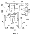
- Power supply circuit is the gas discharge lamp, especially in the form of a high-pressure gas discharge lamp directly connected to the output terminals 21 and 22. Rather, there is usually in between, as in the exemplary embodiment according to 2, an H-bridge circuit 200 is inserted.
- This H-bridge circuit 200 preferably contains FET transistors as Switches 201-204. These FET transistors are against Surges sensitive and therefore to be prevented.
- At 1 it may occasionally occur that between turning on and effectively lighting the lamp second voltage U + alone is so great that the between the Voltage difference is the permissible Overvoltage exceeded. This difference in voltage settles from the values of the two partial voltages U- and U + together too high a contribution can also come from the voltage U-. However, since this is regulated, a limitation of the second voltage U + are taken care of, so that no overvoltage of the H-bridge circuit 200 occurs.
- the further embodiment shown in FIG. invention provides for an application to limit the voltage U + with a load, especially in the form of a voltage divider with resistors 205 and 206 before that between the Output terminal 22 and ground potential 26 is set and the associated output 22 charged.
- the tap of the Voltage divider takes place between the two resistors 205 and 206 via a line 207, which is the input to a microcontroller 208 is supplied, which serves as a control circuit. This creates an output signal, in particular a digital output signal, on line 209, which is fed to a signal converter 251.
- This signal converter 251 generates a line 230 therefrom Control signal for the switch 29, the when closing Resistor 28 as a current load of the temporarily effective Load to DC-DC converter 210 connects.
- the signal converter 251 is via an auxiliary resistor 252 coupled to the voltage U-.
- a comparator 260 is provided, the input of which Line 261 is supplied with a reference voltage as a threshold is. On line 227, the one at the connection point Voltage divider, the current value of the voltage U-dem Comparator 260 supplied.
- the voltage divider consists of the two resistors 262 and 263 connected in series between the Voltage U and a reference voltage source 264 switched are.
- the reference voltage can e.g. B. 5 volts.
- the Result of comparison of comparator 260 between the Reference voltage 261 and the current value of U on line 227 is connected to a control arrangement 214 via an output 265 given. This provides the clock signals on line 15 for the Converter 210 ready.
- Switch 270 provided by a signal on a line 271 is opened or closed by the microcontroller 208.
- This switch 270 is the one according to the invention Embodiment regulated second voltage U + then from the output 22 separated when it is no longer needed there. This is at the preferred application, for example, when the Gas discharge lamp has ignited and not a high one Ignition supply voltage is more needed.
- the earth potential 26 is present. It is over
- a Verpoldiode 272 with its cathode to the Output terminal 22 and with its anode connected to ground potential 26. This arrangement is so because the other Output terminal 21, the negative voltage U- is present, which then Operating voltage to the H-bridge circuit and from there to the Consumer, preferably a high-pressure gas discharge lamp, emits.
- H-bridge circuit 200 is shown connected.
- This H-bridge circuit points between its two switches 201 and 203 a consumer terminal 222 and between their two switches 202 and 204 a consumer terminal 221 on. Is between these consumer terminals 221 and 222 the output voltage Ua on z.
- the particular advantages of the embodiment according to FIG. 2 are watch that the regulation of the second voltage U + very is easy to implement, little additional effort and additional Components required.
- the at least temporarily effective load which is provided to quickly reach the partial voltages also used to regulate the second voltage U +.
- the regulation of the partial voltage U + described above can be used as Upward regulation can be called, because to achieve the Setpoint value, the temporarily effective converter load 28 Increasing the clocking and thus the voltage increase of U + is used.
- 3 is in a modified 2 shows a possible embodiment for a downward regulation is shown.
- the converter 210 over the Block diode 20 clocked energy charges the smoothing capacitor 24 on. This is in front of the switch 270. Behind the switch 270 a further capacitor 350 is arranged, which when closing of switch 270 by a signal on line 271 which is from Microcontroller 208 is provided, the charge and thus the Voltage from capacitor 24 also takes over and as another Buffer or smoothing capacitor works.
- FIG. 4 is an embodiment for the at least temporarily effective load applied to the DC-DC converter 10 or 210 can be connected.
- the resistor 28 is loaded by a switch 29 Transistor 429 between ground potential 26 and voltage U supply or switched off.
- a digital signal 400 which comes from the microcontroller 208 and pulse-shaped is shown, via a Zener diode 401 and a resistor 402 led to the base 403 of the transistor 429.
- a cheap one Pulse-to-pause ratio is approx. 1 ⁇ 4 "on” to 3 ⁇ 4 "off”. This is in the representation of the digital signal 400 by the Combination of solid and dotted pulses shown. According to a numerical example, this ratio can then can be achieved if, as in the exemplary embodiment according to FIG. 2, the value for resistor 205 is about 500 kohm and the value for resistor 206 is approximately 7.5 kOhm.
- transistor 429 of the type When realizing the temporarily effective load, in addition to of the above-explained, various solutions can be chosen.
- transistor 429 of the type it is possible to use transistor 429 of the type to fully control or regulate the two-point control lock. Resistor 28 is thus either completely closed or completely switched off. It is also possible to use a transistor Pulse width modulation signal according to the selected one Switch on pulse width more or less long. Accordingly the resistor 28 acts on the clocking of the clock for a longer or shorter period Converter 10 and 210 a.
- Another implementation option consists of a variable load resistance as at least to provide temporarily effective load. This can be done with Using the drain-source resistance of a FET transistor respectively. The value of this resistance depends on the amount the gate-source voltage.
- the invention enables two with simple means Voltages for supplying a consumer with very to provide different load conditions that queue very quickly after switching on. This is particularly so when used for the supply of the ignition device for the rapid provision of a sufficiently high Ignition supply voltage, as well as for a regulated one Operating voltage of a gas discharge lamp, in particular a high pressure gas discharge lamp of crucial Importance.
Landscapes
- Engineering & Computer Science (AREA)
- Power Engineering (AREA)
- Dc-Dc Converters (AREA)
- Circuit Arrangements For Discharge Lamps (AREA)
Abstract
Claims (11)
- Circuit d'alimentation en courant, cadencé, comprenant une charge indépendante du consommateur et qui est active au moins périodiquement, notamment pour l'alimentation en énergie de consommateurs constitués par des lampes à décharge de gaz, un transmetteur (11) avec un transformateur de tension continu/continu (10, 210), un moyen de commutation (12) pour relier le transformateur (10, 210) à une source de tension continue (13) et un dispositif de commande (14, 214) qui en fonction d'un état de charge existant en sortie, fournit des signaux de commutation (15) pour le moyen de commutation (12),
caractérisé en ce quele convertisseur (11) du transformateur de tension continu/continu (10, 210) est réalisé pour fournir deux tensions (U+, U-) de polarités et d'amplitudes différentes en sortie,au moins l'une (U-) de ces tensions étant régulée et servant à l'alimentation pendant le fonctionnement du consommateur et,la charge active au moins périodiquement (28) peut être branchée sur la tension régulée (U-). - Circuit d'alimentation en courant, cadencé, selon la revendication 1,
caractérisé en ce quela seconde tension (U-) est également régulée,celle-ci est mise à une charge permettant de déterminer la valeur actuelle de la seconde tension (U-), et cette valeur est appliquée à un circuit de régulation (208) qui, en fonction de la valeur constatée de la seconde tension (U-) branche ou coupe la charge active périodiquement (28). - Circuit d'alimentation en courant, cadencé selon la revendication 2,
caractérisé en ce quela charge est constituée par un diviseur de tension (205, 206) dont la prise de diviseur (207) est reliée au circuit de régulation (208). - Circuit d'alimentation en courant, cadencé selon la revendication 3,
caractérisé en ce qu'en parallèle au diviseur de tension (205, 206), on a le montage en série d'une résistance (351) et d'un transistor (352) débloqués par le circuit de régulation (208) lorsque la valeur actuelle de la seconde tension (U+) prise sur le diviseur de tension (205, 206) dépasse la valeur seuil. - Circuit d'alimentation en courant, cadencé, selon les revendications 3 ou 4,
caractérisé en ce quele diviseur de tension (205, 206) est dimensionné pour que le rapport de travail (impulsion/pause) de coupure de la charge active périodiquement (28) ne reste pas trop faible pour permettre notamment une régulation dans les deux directions. - Circuit d'alimentation en courant, cadencé, selon l'une quelconque des revendications précédentes,
caractérisé en ce quela charge (28) active périodiquement peut être coupée ou branchée avec une résistance variable. - Circuit d'alimentation en courant, cadencé selon la revendication 6,
caractérisé en ce quela charge active périodiquement est formée du montage en série d'une résistance ohmique (28) et d'un transistor (429) qui peut être coupé et branché à la manière d'une régulation en deux points ou qui est branché plus ou moins longtemps par un signal à modulation de largeur d'impulsion correspondant à la largeur d'impulsion. - Circuit d'alimentation en courant, cadencé selon la revendication 6,
caractérisé en ce quela charge active périodiquement (28) se compose d'une résistance de charge variable notamment de la résistance drain-source d'un transistor à effet de champ FET, la valeur de la résistance dépendant de l'amplitude de la tension grille-source. - Circuit d'alimentation en courant, cadencé selon l'une quelconque des revendications précédentes,
caractérisé en ce quepour la régulation de ou des tensions régulées (U- ou U+, U-), il est prévu un microcontrôleur (208) qui agit sur le moyen de commutation (12) du transformateur de tension continu/continu (10, 210). - Circuit d'alimentation en courant, cadencé selon l'une quelconque des revendications précédentes,
caractérisé en ce qu'après le branchement complet et la mise en route du consommateur, celle des deux tensions de préférence la tension non régulée ou celle qui a l'amplitude la plus élevée (U+), peut être coupée par un interrupteur (270). - Circuit d'alimentation en courant, cadencé selon l'une quelconque précédentes,
caractériséà l'utilisation dans l'appareil de commande pour l'alimentation en énergie de lampes à décharge de gaz à haute pression, ces lampes équipant notamment des projecteurs de véhicules automobiles.
Applications Claiming Priority (3)
| Application Number | Priority Date | Filing Date | Title |
|---|---|---|---|
| DE19536064 | 1995-09-28 | ||
| DE19536064A DE19536064A1 (de) | 1995-09-28 | 1995-09-28 | Getaktete Stromversorgungsschaltung mit einer von einem Verbraucher unabhängigen, zumindest zeitweise wirksamen Last |
| PCT/DE1996/001153 WO1997012500A1 (fr) | 1995-09-28 | 1996-06-28 | Circuit d'alimentation cadence a charge au moins temporairement active, independante d'un consommateur |
Publications (2)
| Publication Number | Publication Date |
|---|---|
| EP0852895A1 EP0852895A1 (fr) | 1998-07-15 |
| EP0852895B1 true EP0852895B1 (fr) | 1999-04-28 |
Family
ID=7773406
Family Applications (1)
| Application Number | Title | Priority Date | Filing Date |
|---|---|---|---|
| EP96920725A Expired - Lifetime EP0852895B1 (fr) | 1995-09-28 | 1996-06-28 | Circuit d'alimentation cadence a charge au moins temporairement active, independante d'un consommateur |
Country Status (6)
| Country | Link |
|---|---|
| US (1) | US6005302A (fr) |
| EP (1) | EP0852895B1 (fr) |
| JP (1) | JP3923082B2 (fr) |
| KR (1) | KR19990063794A (fr) |
| DE (2) | DE19536064A1 (fr) |
| WO (1) | WO1997012500A1 (fr) |
Families Citing this family (7)
| Publication number | Priority date | Publication date | Assignee | Title |
|---|---|---|---|---|
| DE19702687C1 (de) * | 1997-01-25 | 1998-08-06 | Bosch Gmbh Robert | Anordnung zum Schutz gegen Übertemperatur eines Steuergeräts für Gasentladungslampen |
| DE19732098A1 (de) * | 1997-07-25 | 1999-01-28 | Bosch Gmbh Robert | Steuerschaltung für einen Gleichstrommotor |
| IT1305660B1 (it) * | 1998-02-16 | 2001-05-15 | Zeltron Spa | Alimentatore elettrico perfezionato |
| WO2000014862A1 (fr) * | 1998-09-07 | 2000-03-16 | Koninklijke Philips Electronics N.V. | Montage de circuit |
| JP3806279B2 (ja) * | 2000-01-20 | 2006-08-09 | 株式会社小糸製作所 | 放電灯点灯回路 |
| AT411506B (de) * | 2000-10-02 | 2004-01-26 | Siemens Ag Oesterreich | Schaltwandler |
| US20210380060A1 (en) * | 2020-06-04 | 2021-12-09 | Veoneer Us, Inc. | Sensor communication discrete control considering emc compliance for restraint control module |
Family Cites Families (9)
| Publication number | Priority date | Publication date | Assignee | Title |
|---|---|---|---|---|
| JPS59180994A (ja) * | 1983-03-30 | 1984-10-15 | 東芝ライテック株式会社 | 放電灯点灯装置 |
| US4586119A (en) * | 1984-04-16 | 1986-04-29 | Itt Corporation | Off-line switching mode power supply |
| DE3508895A1 (de) * | 1985-03-13 | 1986-09-18 | ANT Nachrichtentechnik GmbH, 7150 Backnang | Gleichspannungswandler mit mehreren geregelten ausgaengen |
| DE3604716A1 (de) * | 1986-02-14 | 1987-08-20 | Nixdorf Computer Ag | Schaltungsanordnung zur steuerung des laengsschaltgliedes eines getakteten stromversorgungsgeraets |
| DE3633518A1 (de) * | 1986-10-02 | 1988-04-14 | Philips Patentverwaltung | Getakteter gleichspannungswandler |
| DE3923710A1 (de) * | 1989-07-18 | 1991-01-24 | Philips Patentverwaltung | Stromversorgungseinrichtung mit gleichspannungsueberwachungsschaltung |
| DE4231968A1 (de) * | 1992-09-24 | 1994-03-31 | Bosch Gmbh Robert | Getaktete Stromversorgungsschaltung |
| DE4342590A1 (de) * | 1993-12-14 | 1995-06-22 | Bosch Gmbh Robert | Getaktete Stromversorgung |
| DE4424800A1 (de) * | 1994-07-14 | 1996-01-18 | Philips Patentverwaltung | Schaltungsanordnung zum Liefern von Speisespannungen |
-
1995
- 1995-09-28 DE DE19536064A patent/DE19536064A1/de not_active Withdrawn
-
1996
- 1996-06-28 KR KR1019980702261A patent/KR19990063794A/ko not_active Application Discontinuation
- 1996-06-28 EP EP96920725A patent/EP0852895B1/fr not_active Expired - Lifetime
- 1996-06-28 US US09/043,978 patent/US6005302A/en not_active Expired - Fee Related
- 1996-06-28 JP JP51304897A patent/JP3923082B2/ja not_active Expired - Fee Related
- 1996-06-28 WO PCT/DE1996/001153 patent/WO1997012500A1/fr not_active Application Discontinuation
- 1996-06-28 DE DE59601786T patent/DE59601786D1/de not_active Expired - Lifetime
Also Published As
| Publication number | Publication date |
|---|---|
| US6005302A (en) | 1999-12-21 |
| JP3923082B2 (ja) | 2007-05-30 |
| EP0852895A1 (fr) | 1998-07-15 |
| WO1997012500A1 (fr) | 1997-04-03 |
| DE19536064A1 (de) | 1997-04-03 |
| KR19990063794A (ko) | 1999-07-26 |
| JPH11511588A (ja) | 1999-10-05 |
| DE59601786D1 (de) | 1999-06-02 |
Similar Documents
| Publication | Publication Date | Title |
|---|---|---|
| DE102005035665A1 (de) | Zündanlage für eine Brennkraftmaschine | |
| EP1675245A2 (fr) | Circuit pour la diminution rapide du courant de roue libre dans l'enroulement d'excitation d'un générateur | |
| WO2012130649A1 (fr) | Procédé et dispositif de prolongement de la durée de combustion d'une étincelle allumée par une bougie d'allumage dans un moteur à combustion interne | |
| EP0811306B1 (fr) | Circuit d'amor age pour lampe a decharge a haute pression | |
| EP0664602B1 (fr) | Convertisseur à récupération avec tension de sortie régulée | |
| EP0314681B1 (fr) | Etage final de circuit a pont | |
| EP3069007A1 (fr) | Système d'allumage et procédé pour faire fonctionner un système d'allumage | |
| DE3107301A1 (de) | Plasmastrahl-zuendsystem | |
| EP0852895B1 (fr) | Circuit d'alimentation cadence a charge au moins temporairement active, independante d'un consommateur | |
| WO2014056661A2 (fr) | Dispositif de conversion de tension ainsi que réseau de bord comprenant un tel dispositif | |
| EP2129897B1 (fr) | Circuit de commande et procédé de commande d'un élément piezoélectrique | |
| DE10143726B4 (de) | Fahrzeuggeneratorsteuervorrichtung | |
| DE102013201815A1 (de) | Zündsystem | |
| DE3404245A1 (de) | Hochspannungs-generatorschaltung fuer ein kraftfahrzeugzuendsystem | |
| DE4446532A1 (de) | Stromversorgungsschaltung | |
| DE3238899A1 (de) | Kurzschlussfeste ansteuerschaltung fuer einen elektrischen verbraucher | |
| DE10314566A1 (de) | Ansteuerschaltung für piezoelektrische Bauteile | |
| DE10155972A1 (de) | Zündanlage und Verfahren zum Betreiben einer Zündanlage | |
| EP0266743B1 (fr) | Disposition de circuit pour produire une tension d'alimentation interne dans une alimentation de courant à découpage | |
| LU101883B1 (de) | Schaltungsanordnung zum Begrenzen eines Einschaltstroms | |
| DE10328623B4 (de) | Konverterschaltung und Brennkraftmaschine | |
| WO2010108899A1 (fr) | Convertisseur de tension continue pour un véhicule automobile | |
| EP0690552A2 (fr) | Convertisseur de tension électronique | |
| DE10055077A1 (de) | Vorrichtung zum Verpolschutz elektrischer Komponenten | |
| DE112022000785T5 (de) | Schaltvorrichtung, elektronisches gerät und fahrzeug |
Legal Events
| Date | Code | Title | Description |
|---|---|---|---|
| PUAI | Public reference made under article 153(3) epc to a published international application that has entered the european phase |
Free format text: ORIGINAL CODE: 0009012 |
|
| 17P | Request for examination filed |
Effective date: 19980428 |
|
| AK | Designated contracting states |
Kind code of ref document: A1 Designated state(s): DE FR GB IT |
|
| GRAG | Despatch of communication of intention to grant |
Free format text: ORIGINAL CODE: EPIDOS AGRA |
|
| 17Q | First examination report despatched |
Effective date: 19980813 |
|
| GRAG | Despatch of communication of intention to grant |
Free format text: ORIGINAL CODE: EPIDOS AGRA |
|
| GRAH | Despatch of communication of intention to grant a patent |
Free format text: ORIGINAL CODE: EPIDOS IGRA |
|
| GRAH | Despatch of communication of intention to grant a patent |
Free format text: ORIGINAL CODE: EPIDOS IGRA |
|
| GRAA | (expected) grant |
Free format text: ORIGINAL CODE: 0009210 |
|
| AK | Designated contracting states |
Kind code of ref document: B1 Designated state(s): DE FR GB IT |
|
| REF | Corresponds to: |
Ref document number: 59601786 Country of ref document: DE Date of ref document: 19990602 |
|
| ET | Fr: translation filed | ||
| GBT | Gb: translation of ep patent filed (gb section 77(6)(a)/1977) |
Effective date: 19990707 |
|
| PLBE | No opposition filed within time limit |
Free format text: ORIGINAL CODE: 0009261 |
|
| STAA | Information on the status of an ep patent application or granted ep patent |
Free format text: STATUS: NO OPPOSITION FILED WITHIN TIME LIMIT |
|
| 26N | No opposition filed | ||
| PGFP | Annual fee paid to national office [announced via postgrant information from national office to epo] |
Ref country code: GB Payment date: 20000619 Year of fee payment: 5 |
|
| PG25 | Lapsed in a contracting state [announced via postgrant information from national office to epo] |
Ref country code: GB Free format text: LAPSE BECAUSE OF NON-PAYMENT OF DUE FEES Effective date: 20010628 |
|
| GBPC | Gb: european patent ceased through non-payment of renewal fee |
Effective date: 20010628 |
|
| PGFP | Annual fee paid to national office [announced via postgrant information from national office to epo] |
Ref country code: FR Payment date: 20030618 Year of fee payment: 8 |
|
| PG25 | Lapsed in a contracting state [announced via postgrant information from national office to epo] |
Ref country code: FR Free format text: LAPSE BECAUSE OF NON-PAYMENT OF DUE FEES Effective date: 20050228 |
|
| REG | Reference to a national code |
Ref country code: FR Ref legal event code: ST |
|
| PG25 | Lapsed in a contracting state [announced via postgrant information from national office to epo] |
Ref country code: IT Free format text: LAPSE BECAUSE OF NON-PAYMENT OF DUE FEES Effective date: 20050628 |
|
| PGFP | Annual fee paid to national office [announced via postgrant information from national office to epo] |
Ref country code: DE Payment date: 20110823 Year of fee payment: 16 |
|
| REG | Reference to a national code |
Ref country code: DE Ref legal event code: R119 Ref document number: 59601786 Country of ref document: DE Effective date: 20130101 |
|
| PG25 | Lapsed in a contracting state [announced via postgrant information from national office to epo] |
Ref country code: DE Free format text: LAPSE BECAUSE OF NON-PAYMENT OF DUE FEES Effective date: 20130101 |