EP0852844B1 - Dispositif de circuit comprenant un etage d'amplification de puissance - Google Patents
Dispositif de circuit comprenant un etage d'amplification de puissance Download PDFInfo
- Publication number
- EP0852844B1 EP0852844B1 EP97924212A EP97924212A EP0852844B1 EP 0852844 B1 EP0852844 B1 EP 0852844B1 EP 97924212 A EP97924212 A EP 97924212A EP 97924212 A EP97924212 A EP 97924212A EP 0852844 B1 EP0852844 B1 EP 0852844B1
- Authority
- EP
- European Patent Office
- Prior art keywords
- power amplifier
- output
- gain
- input
- coupled
- Prior art date
- Legal status (The legal status is an assumption and is not a legal conclusion. Google has not performed a legal analysis and makes no representation as to the accuracy of the status listed.)
- Expired - Lifetime
Links
- 238000000605 extraction Methods 0.000 abstract 1
- 230000005540 biological transmission Effects 0.000 description 2
- 230000004048 modification Effects 0.000 description 2
- 238000012986 modification Methods 0.000 description 2
- 230000032683 aging Effects 0.000 description 1
- 230000003321 amplification Effects 0.000 description 1
- 238000011156 evaluation Methods 0.000 description 1
- 238000005259 measurement Methods 0.000 description 1
- 238000003199 nucleic acid amplification method Methods 0.000 description 1
Images
Classifications
-
- H—ELECTRICITY
- H03—ELECTRONIC CIRCUITRY
- H03F—AMPLIFIERS
- H03F1/00—Details of amplifiers with only discharge tubes, only semiconductor devices or only unspecified devices as amplifying elements
- H03F1/32—Modifications of amplifiers to reduce non-linear distortion
- H03F1/3241—Modifications of amplifiers to reduce non-linear distortion using predistortion circuits
-
- H—ELECTRICITY
- H03—ELECTRONIC CIRCUITRY
- H03F—AMPLIFIERS
- H03F2200/00—Indexing scheme relating to amplifiers
- H03F2200/372—Noise reduction and elimination in amplifier
Definitions
- Circuit arrangement comprising a power amplifier stage.
- the invention relates to a circuit arrangement according to the preamble of claim 1.
- the gain factors of the gain control elements included as a first gain control element comprised in a forward gain path and as a second gain control element comprised in a feedback path disclosed in the European Patent Application 0 638 994 are varied inversely, so that their product remains substantially constant, there is additionally achieved that the feedback loop (formed by said forward gain path, said feedback path and a combining means for combining an output of the feedback loop with a signal applied to an input of the forward gain path, this combining means in the following also being referred to as re-combining stage,) formed by the circuit arrangement is also operated with different powers transmitted via the power amplifier stage with constant signal levels on the signal input and is thus capable of operating at a signal level to which it is optimally designed.
- a Cartesian amplifier is known provided with a means of controlling its output power comprising a controllable attenuator in the amplifier forward path and a controllable amplifier in the feedback path.
- a control signal representing the required power level is applied to the attenuator and controllable amplifier and, in response thereto the degrees of attenuation and amplification are varied in inverse proportion to one another.
- the first gain control element as disclosed in the European Patent Application 0 638 994 is formed by an adjustable delay element which is preceded in the forward gain path by a low noise amplifying means, in the following also being referred to as low-noise amplifier stage which has a substantially constant gain factor. Losses in downstream elements in the forward gain path are overcompensated for by the gain factor of the low-noise amplifier stage.
- the low-noise increase of the signal level in the low-noise amplifier stage provides an improvement of the signal-to-noise ratio in this part of the forward gain path.
- the invention is particularly advantageous if the circuit arrangement is embodied as a Cartesian loop.
- a summing means in the following also being referred to as summing stage is inserted into the forward gain path between the quadrature related frequency up-converters, in the following also being referred to as up-converters or mixers, respectively, for the Cartesian components of the signal to be amplified and the power amplifier stage.
- Losses occurring in this summing stage are overcompensated for according to this embodiment of the invention as disclosed in claim 2 in that between the mixers for the quadrature components of the signal to be amplified and the summing stage, low-noise amplifiers are inserted which form the low-noise amplifier stage in the forward gain path. This improves the noise characteristic in the range of the summing stage.
- the control circuit does not only maintain the product of the gain factors of the first and second gain control elements at a constant level, but also the gain factor of the power amplifier stage is incorporated in this product which is maintained at a constant level.
- variations in the gain of the power amplifier stage caused, for example, by temperature variations or ageing, can be compensated for, so that the overall transmission behaviour of the circuit arrangement becomes more constant.
- a circuit arrangement according to the invention is used within a transmitter power amplifier of a transmitter apparatus.
- a transmitter as disclosed and claimed in claims 3and 4 and can advantageously be used in a telecommunication apparatus as disclosed and claimed in claims 5 and 6.
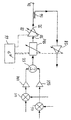
- the forward gain path comprises the mixers 44 and 46 for the quadrature components of the signal to be amplified.
- the output signals of the mixers 44 and 46 are applied according to the present invention to a summing stage 52 via a low-noise amplifier 441, 461 respectively, and additively combined in that stage.
- the sum signal goes via an adjustable attenuation element 541 to an input 30 of the power amplifier stage 28 and from the amplifier stage output 32 via a coupler 56 partly to an output 24 which can be connected to an antenna and partly to the second gain control element 58.
- the adjustable attenuation element 541 and the second gain control element 58 are varied inversely by a control circuit 66 in the manner known from EP 0 638 994 A1.
- This control circuit 66 may preferably comprise a microprocessor.
- the power amplifier stage 28 can be controlled by the control circuit 66.
- the control circuit varies the gain factors of the adjustable attenuation element 541 (first gain control element), of the second gain control element 58 and of the power amplifier stage 28 in such a way that its product remains substantially constant.
- the control circuit can also make a measurement of the gain factor of the power amplifier stage i.e. an evaluation of the ratio of the signal amplitudes on the output 32 and input 30. The thus established actual value of the gain factor of the power amplifier stage may then be used as a basis for the setting of the gain factor of the two gain control elements.
Landscapes
- Physics & Mathematics (AREA)
- Nonlinear Science (AREA)
- Engineering & Computer Science (AREA)
- Power Engineering (AREA)
- Amplifiers (AREA)
- Transmitters (AREA)
- Control Of Amplification And Gain Control (AREA)
Abstract
Claims (6)
- Dispositif de circuit comprenant une voie de gain direct dotée d'un amplificateur de puissance (28) ayant une entrée (30) et une sortie (32) et d'une boucle de réaction comprenant des moyens (56) pour dériver une partie de la sortie (32) de l'amplificateur de puissance et un étage de fonction de réaction combinant des moyens pour combiner une sortie de la boucle de réaction avec un signal appliqué à une entrée de la voie de gain direct, la voie de gain direct comprenant par ailleurs un amplificateur à faible bruit (441, 461) et une sortie couplée à l'entrée (30) de l'amplificateur de puissance (28), la voie de réaction comprenant par ailleurs un élément de réglage du gain (58) et un circuit de commande (66) pour commander l'élément d'atténuation réglable (541) et l'élément de réglage du gain (58),
caractérisé en ce que l'amplificateur de puissance (28) possède une entrée pour un signal de réglage du gain fourni par le circuit de commande (66) et que le circuit de commande (66) commande l'élément d'atténuation réglable (541) et les gains de l'élément du réglage du gain (58) et l'amplificateur de puissance (28) de telle sorte que leur produit ait une valeur essentiellement constante. - Dispositif de circuit selon la revendication 1, possédant une structure de boucle cartésienne,
dans lequel la voie de gain direct comprend des premier et deuxième convertisseurs élévateurs de fréquence (44, 46) liés à la quadrature couplés aux moyens de combinaison, les moyens amplificateurs (441, 461) à faible bruit comprenant des amplificateurs à faible bruit (441 et 461, respectivement) couplés respectivement à des sorties des premier (44) et deuxième (46) convertisseurs élévateurs de fréquence et dans lequel les moyens additionneurs (52) sont couplés aux sorties desdits amplificateurs à faible bruit (441, 461) et à l'entrée de l'élément d'atténuation réglable (541). - Emetteur comprenant une voie de gain direct doté d'un amplificateur de puissance (28) possédant une entrée (30) et une sortie (32) et d'une boucle de réaction comprenant des moyens (56) pour dériver une partie de la sortie (32) de l'amplificateur de puissance et un étage de fonction de réaction, des moyens de combinaison pour combiner une sortie de la boucle de réaction avec un signal de modulation appliqué à une entrée de la voie de gain direct, la voie de gain direct comprenant par ailleurs un moyen d'amplification à faible bruit (441, 461) possédant un facteur de gain essentiellement constant et un élément d'atténuation réglable (541) possédant une entrée couplée à une sortie des moyens d'amplification à faible bruit (441, 461) et une sortie couplée à l'entrée (30) de l'amplificateur de puissance (28, la voie de réaction étant par ailleurs dotée d'un élément de réglage du gain (58) et d'un circuit de commande (66) pour commander l'élément d'atténuation réglable (541) et l'élément de réglage du gain (58),
caractérisé en ce que l'amplificateur de puissance (28) possède une entrée pour un signal de réglage du gain fourni par le circuit de commande (66) et que le circuit de commande (66) commande l'élément d'atténuation réglable (541) et les gains de l'élément de réglage du gain (58) et l'amplificateur de puissance (28) de telle sorte que le produit ait une valeur essentiellement constante. - Emetteur selon la revendication 3, possédant une structure de boucle cartésienne, dans lequel une voie de gain direct comprend des premier et deuxième convertisseurs élévateurs de fréquence (44, 46) liés à la quadrature et couplés aux moyens de combinaison, les moyens amplificateurs à faible bruit (441, 461) comprenant des amplificateurs à faible bruit (441 et 461, respectivement), couplés respectivement aux sorties des premier (44) et deuxième (46) convertisseurs élévateurs de fréquence et dans lequel les moyens additionneurs (52) sont couplés aux sorties desdits amplificateurs à faible bruit (441 et 461 respectivement) et à l'entrée de l'élément d'atténuation réglable (541).
- Appareil de télécommunication comprenant un radio-émetteur doté d'une voie de gain direct comprenant un amplificateur de puissance (28) muni d'une entrée (30) et d'une sortie (32), de moyens de propagation du signal couplés à ladite sortie et d'une boucle de réaction comprenant des moyens (56) pour dériver une partie de la sortie (32) de l'amplificateur de puissance et un étage de fonction de réaction, combinant des moyens pour combiner une sortie de la boucle de réaction avec un signal de modulation appliqué à une entrée de la voie du gain direct, la voie de gain direct comprenant par ailleurs des amplificateurs à faible bruit (441, 461) ayant un facteur de gain essentiellement constant et un élément d'atténuation réglable (541) ayant une entrée couplée à une sortie des amplificateurs à faible bruit (441, 461) et une sortie couplée à l'entrée (340) de l'amplificateur de puissance (28), la voie de réaction comprenant par ailleurs un élément de réglage du gain (58) et un circuit de commande (66) pour commander l'élément d'atténuation réglable (541) et l'élément de réglage du gain (58),
caractérisé en ce que l'amplificateur de puissance (28) a une entrée pour un signal de réglage du gain fourni par le circuit de commande (66) et que le circuit de commande (66) commande l'élément d'atténuation réglable (541) et les gains de l'élément de réglage du gain (58) et de l'amplificateur de puissance (28) de telle sorte que leur produit ait une valeur essentiellement constante. - Appareil de télécommunication selon la revendication 5 ayant une structure en boucle cartésienne,
dans lequel la voie de gain direct comprend des premier et deuxième convertisseurs élévateurs de fréquence liés à la quadrature couplés aux moyens de combinaison, les moyens amplificateurs à faible bruit (441, 461) comprenant des amplificateurs à faible bruit (44 et 461, respectivement), couplés respectivement aux sorties des premier (44) et deuxième (46) convertisseurs élévateurs de fréquence et dans lequel les moyens d'addition (52) sont couplés aux sorties desdits amplificateurs à faible bruit (441 et 461, respectivement) et à l'entrée de l'élément d'atténuation (541) réglable.
Priority Applications (1)
| Application Number | Priority Date | Filing Date | Title |
|---|---|---|---|
| EP97924212A EP0852844B1 (fr) | 1996-06-28 | 1997-06-18 | Dispositif de circuit comprenant un etage d'amplification de puissance |
Applications Claiming Priority (4)
| Application Number | Priority Date | Filing Date | Title |
|---|---|---|---|
| EP96110470 | 1996-06-28 | ||
| EP96110470 | 1996-06-28 | ||
| EP97924212A EP0852844B1 (fr) | 1996-06-28 | 1997-06-18 | Dispositif de circuit comprenant un etage d'amplification de puissance |
| PCT/IB1997/000730 WO1998000907A1 (fr) | 1996-06-28 | 1997-06-18 | Dispositif de circuit comprenant un etage d'amplification de puissance |
Publications (2)
| Publication Number | Publication Date |
|---|---|
| EP0852844A1 EP0852844A1 (fr) | 1998-07-15 |
| EP0852844B1 true EP0852844B1 (fr) | 2003-12-17 |
Family
ID=8222953
Family Applications (1)
| Application Number | Title | Priority Date | Filing Date |
|---|---|---|---|
| EP97924212A Expired - Lifetime EP0852844B1 (fr) | 1996-06-28 | 1997-06-18 | Dispositif de circuit comprenant un etage d'amplification de puissance |
Country Status (5)
| Country | Link |
|---|---|
| US (1) | US6008697A (fr) |
| EP (1) | EP0852844B1 (fr) |
| JP (1) | JP4164565B2 (fr) |
| DE (1) | DE69726833T2 (fr) |
| WO (1) | WO1998000907A1 (fr) |
Families Citing this family (5)
| Publication number | Priority date | Publication date | Assignee | Title |
|---|---|---|---|---|
| US6466628B1 (en) * | 1998-04-18 | 2002-10-15 | Lucent Technologies Inc. | Technique for effectively rendering power amplification and control in wireless communications |
| GB2356756B (en) | 1999-11-25 | 2004-08-11 | Ericsson Telefon Ab L M | Power amplifiers |
| US6670849B1 (en) * | 2000-08-30 | 2003-12-30 | Skyworks Solutions, Inc. | System for closed loop power control using a linear or a non-linear power amplifier |
| FI109059B (fi) * | 2001-02-21 | 2002-05-15 | Nokia Corp | Menetelmä lähettimen häiriöiden vähentämiseksi, lähetin ja radiolaite |
| JP4578169B2 (ja) * | 2004-07-23 | 2010-11-10 | 三洋電機株式会社 | 自動レベル調整回路 |
Family Cites Families (4)
| Publication number | Priority date | Publication date | Assignee | Title |
|---|---|---|---|---|
| JP2540377B2 (ja) * | 1990-07-04 | 1996-10-02 | 三菱電機株式会社 | 自動出力電力制御装置 |
| FI97177C (fi) * | 1993-09-06 | 1996-10-25 | Nokia Telecommunications Oy | Menetelmä ja järjestely suurtaajuustehovahvistimen toiminnan ohjaamiseen |
| GB9316869D0 (en) * | 1993-08-13 | 1993-09-29 | Philips Electronics Uk Ltd | Transmitter and power amplifier therefor |
| GB9320078D0 (en) * | 1993-09-29 | 1993-11-17 | Linear Modulation Tech | Cartesian amplifier power control and related applications |
-
1997
- 1997-06-18 JP JP50394198A patent/JP4164565B2/ja not_active Expired - Fee Related
- 1997-06-18 US US09/029,528 patent/US6008697A/en not_active Expired - Lifetime
- 1997-06-18 DE DE69726833T patent/DE69726833T2/de not_active Expired - Lifetime
- 1997-06-18 WO PCT/IB1997/000730 patent/WO1998000907A1/fr not_active Ceased
- 1997-06-18 EP EP97924212A patent/EP0852844B1/fr not_active Expired - Lifetime
Also Published As
| Publication number | Publication date |
|---|---|
| EP0852844A1 (fr) | 1998-07-15 |
| JPH11513216A (ja) | 1999-11-09 |
| DE69726833T2 (de) | 2004-10-07 |
| US6008697A (en) | 1999-12-28 |
| WO1998000907A1 (fr) | 1998-01-08 |
| JP4164565B2 (ja) | 2008-10-15 |
| DE69726833D1 (de) | 2004-01-29 |
Similar Documents
| Publication | Publication Date | Title |
|---|---|---|
| US5155448A (en) | Feed-forward amplifier having increased compression point | |
| US5291147A (en) | Power booster for a radio telephone | |
| CA2089617C (fr) | Circuit de commande automatique de correction aval de distorsion non lineaire pour amplificateur | |
| EP0869606A2 (fr) | Amplificateur à boucle de contre-réaction de type aval | |
| EP0397444A2 (fr) | Circuit pour élargir l'étendue du contrôle de la puissance dans un émetteur | |
| WO1998057442A3 (fr) | Systeme et procede concernant une unite radio | |
| EP0895351A3 (fr) | Dispositif de contrôle de gain automatique pour micro-ondes | |
| US5977825A (en) | Electronic circuit for linearization of an amplifier | |
| KR19980021121A (ko) | 무선통신시스템의 전력조절 회로 및 방법 | |
| EP0852844B1 (fr) | Dispositif de circuit comprenant un etage d'amplification de puissance | |
| US7095988B2 (en) | Apparatus for linear transmitter with improved loop gain stabilization | |
| EP0986168A2 (fr) | Circuit de réduction de distorsion par contre-réaction du type aval sans pilote | |
| KR20010010813A (ko) | Rf 중계기의 전후방감쇄 자동조절장치 및 그 방법 | |
| JP2001237651A (ja) | 電力増幅装置 | |
| US7076218B2 (en) | Control method and circuit for using a heterojunction bipolar transistor power amplifier in a zero intermediate frequency architecture transmitter | |
| JP2922524B2 (ja) | 電力増幅装置 | |
| US8559896B2 (en) | System and method for radio power level control | |
| US4837522A (en) | Noise reducer for microwave amplifier | |
| JP2780439B2 (ja) | 送信出力制御方式 | |
| KR100318480B1 (ko) | 동적출력레벨을갖는이동통신단말기 | |
| KR930006650B1 (ko) | 고전력 증폭장치 | |
| KR100689536B1 (ko) | 이동통신시스템에서 전류소모를 줄이기 위한 송신장치 | |
| JPH0897642A (ja) | 低歪み増幅器、多段増幅器および移動体通信用基地局 | |
| KR200153869Y1 (ko) | 초고주파 신호출력 이득제어회로 | |
| KR940002969B1 (ko) | 고전력 증폭장치 |
Legal Events
| Date | Code | Title | Description |
|---|---|---|---|
| PUAI | Public reference made under article 153(3) epc to a published international application that has entered the european phase |
Free format text: ORIGINAL CODE: 0009012 |
|
| AK | Designated contracting states |
Kind code of ref document: A1 Designated state(s): DE FR GB |
|
| RAP3 | Party data changed (applicant data changed or rights of an application transferred) |
Owner name: PHILIPS PATENTVERWALTUNG GMBH Owner name: KONINKLIJKE PHILIPS ELECTRONICS N.V. |
|
| 17P | Request for examination filed |
Effective date: 19980708 |
|
| RAP3 | Party data changed (applicant data changed or rights of an application transferred) |
Owner name: PHILIPS CORPORATE INTELLECTUAL PROPERTY GMBH Owner name: KONINKLIJKE PHILIPS ELECTRONICS N.V. |
|
| 17Q | First examination report despatched |
Effective date: 20001221 |
|
| RAP1 | Party data changed (applicant data changed or rights of an application transferred) |
Owner name: PHILIPS CORPORATE INTELLECTUAL PROPERTY GMBH Owner name: KONINKLIJKE PHILIPS ELECTRONICS N.V. |
|
| GRAH | Despatch of communication of intention to grant a patent |
Free format text: ORIGINAL CODE: EPIDOS IGRA |
|
| RAP1 | Party data changed (applicant data changed or rights of an application transferred) |
Owner name: PHILIPS INTELLECTUAL PROPERTY & STANDARDS GMBH Owner name: KONINKLIJKE PHILIPS ELECTRONICS N.V. |
|
| GRAS | Grant fee paid |
Free format text: ORIGINAL CODE: EPIDOSNIGR3 |
|
| GRAA | (expected) grant |
Free format text: ORIGINAL CODE: 0009210 |
|
| AK | Designated contracting states |
Kind code of ref document: B1 Designated state(s): DE FR GB |
|
| REG | Reference to a national code |
Ref country code: GB Ref legal event code: FG4D |
|
| REG | Reference to a national code |
Ref country code: GB Ref legal event code: 746 Effective date: 20031222 |
|
| REF | Corresponds to: |
Ref document number: 69726833 Country of ref document: DE Date of ref document: 20040129 Kind code of ref document: P |
|
| ET | Fr: translation filed | ||
| PLBE | No opposition filed within time limit |
Free format text: ORIGINAL CODE: 0009261 |
|
| STAA | Information on the status of an ep patent application or granted ep patent |
Free format text: STATUS: NO OPPOSITION FILED WITHIN TIME LIMIT |
|
| REG | Reference to a national code |
Ref country code: FR Ref legal event code: D6 |
|
| 26N | No opposition filed |
Effective date: 20040920 |
|
| REG | Reference to a national code |
Ref country code: GB Ref legal event code: 732E |
|
| REG | Reference to a national code |
Ref country code: FR Ref legal event code: TP |
|
| REG | Reference to a national code |
Ref country code: FR Ref legal event code: ST Effective date: 20100226 |
|
| PG25 | Lapsed in a contracting state [announced via postgrant information from national office to epo] |
Ref country code: FR Free format text: LAPSE BECAUSE OF NON-PAYMENT OF DUE FEES Effective date: 20090630 |
|
| REG | Reference to a national code |
Ref country code: FR Ref legal event code: D3 |
|
| PGRI | Patent reinstated in contracting state [announced from national office to epo] |
Ref country code: FR Effective date: 20101103 |
|
| PGFP | Annual fee paid to national office [announced via postgrant information from national office to epo] |
Ref country code: GB Payment date: 20120525 Year of fee payment: 16 |
|
| GBPC | Gb: european patent ceased through non-payment of renewal fee |
Effective date: 20130618 |
|
| PG25 | Lapsed in a contracting state [announced via postgrant information from national office to epo] |
Ref country code: GB Free format text: LAPSE BECAUSE OF NON-PAYMENT OF DUE FEES Effective date: 20130618 |
|
| REG | Reference to a national code |
Ref country code: FR Ref legal event code: PLFP Year of fee payment: 20 |
|
| PGFP | Annual fee paid to national office [announced via postgrant information from national office to epo] |
Ref country code: DE Payment date: 20160524 Year of fee payment: 20 |
|
| PGFP | Annual fee paid to national office [announced via postgrant information from national office to epo] |
Ref country code: FR Payment date: 20160526 Year of fee payment: 20 |
|
| REG | Reference to a national code |
Ref country code: DE Ref legal event code: R071 Ref document number: 69726833 Country of ref document: DE |