EP0851578A2 - Filterschaltung - Google Patents
Filterschaltung Download PDFInfo
- Publication number
- EP0851578A2 EP0851578A2 EP97121978A EP97121978A EP0851578A2 EP 0851578 A2 EP0851578 A2 EP 0851578A2 EP 97121978 A EP97121978 A EP 97121978A EP 97121978 A EP97121978 A EP 97121978A EP 0851578 A2 EP0851578 A2 EP 0851578A2
- Authority
- EP
- European Patent Office
- Prior art keywords
- differential
- differential voltage
- transconductor
- voltage input
- output
- Prior art date
- Legal status (The legal status is an assumption and is not a legal conclusion. Google has not performed a legal analysis and makes no representation as to the accuracy of the status listed.)
- Granted
Links
- 239000003990 capacitor Substances 0.000 claims description 43
- 230000005669 field effect Effects 0.000 claims description 5
- 230000005540 biological transmission Effects 0.000 description 9
- 238000010586 diagram Methods 0.000 description 9
- 238000012545 processing Methods 0.000 description 9
- 238000006243 chemical reaction Methods 0.000 description 6
- 238000005516 engineering process Methods 0.000 description 5
- 230000008901 benefit Effects 0.000 description 4
- 230000000694 effects Effects 0.000 description 4
- 238000000034 method Methods 0.000 description 4
- 239000000470 constituent Substances 0.000 description 2
- 230000001419 dependent effect Effects 0.000 description 2
- 238000001914 filtration Methods 0.000 description 2
- 238000004519 manufacturing process Methods 0.000 description 2
- 238000012986 modification Methods 0.000 description 2
- 230000004048 modification Effects 0.000 description 2
- 230000010355 oscillation Effects 0.000 description 2
- 230000005236 sound signal Effects 0.000 description 2
- 238000004364 calculation method Methods 0.000 description 1
- 230000008859 change Effects 0.000 description 1
- 238000007596 consolidation process Methods 0.000 description 1
- 230000003247 decreasing effect Effects 0.000 description 1
- 238000011161 development Methods 0.000 description 1
- 238000000605 extraction Methods 0.000 description 1
- 230000010354 integration Effects 0.000 description 1
- 238000012544 monitoring process Methods 0.000 description 1
- 230000009467 reduction Effects 0.000 description 1
- 239000004065 semiconductor Substances 0.000 description 1
- 230000035945 sensitivity Effects 0.000 description 1
- 239000000758 substrate Substances 0.000 description 1
Images


Classifications
-
- H—ELECTRICITY
- H03—ELECTRONIC CIRCUITRY
- H03H—IMPEDANCE NETWORKS, e.g. RESONANT CIRCUITS; RESONATORS
- H03H11/00—Networks using active elements
- H03H11/02—Multiple-port networks
- H03H11/04—Frequency selective two-port networks
- H03H11/12—Frequency selective two-port networks using amplifiers with feedback
-
- H—ELECTRICITY
- H03—ELECTRONIC CIRCUITRY
- H03H—IMPEDANCE NETWORKS, e.g. RESONANT CIRCUITS; RESONATORS
- H03H11/00—Networks using active elements
- H03H11/02—Multiple-port networks
- H03H11/04—Frequency selective two-port networks
- H03H11/0422—Frequency selective two-port networks using transconductance amplifiers, e.g. gmC filters
-
- H—ELECTRICITY
- H03—ELECTRONIC CIRCUITRY
- H03B—GENERATION OF OSCILLATIONS, DIRECTLY OR BY FREQUENCY-CHANGING, BY CIRCUITS EMPLOYING ACTIVE ELEMENTS WHICH OPERATE IN A NON-SWITCHING MANNER; GENERATION OF NOISE BY SUCH CIRCUITS
- H03B5/00—Generation of oscillations using amplifier with regenerative feedback from output to input
- H03B5/30—Generation of oscillations using amplifier with regenerative feedback from output to input with frequency-determining element being electromechanical resonator
- H03B5/32—Generation of oscillations using amplifier with regenerative feedback from output to input with frequency-determining element being electromechanical resonator being a piezoelectric resonator
- H03B5/36—Generation of oscillations using amplifier with regenerative feedback from output to input with frequency-determining element being electromechanical resonator being a piezoelectric resonator active element in amplifier being semiconductor device
-
- H—ELECTRICITY
- H03—ELECTRONIC CIRCUITRY
- H03F—AMPLIFIERS
- H03F1/00—Details of amplifiers with only discharge tubes, only semiconductor devices or only unspecified devices as amplifying elements
- H03F1/34—Negative-feedback-circuit arrangements with or without positive feedback
-
- H—ELECTRICITY
- H03—ELECTRONIC CIRCUITRY
- H03H—IMPEDANCE NETWORKS, e.g. RESONANT CIRCUITS; RESONATORS
- H03H9/00—Networks comprising electromechanical or electro-acoustic devices; Electromechanical resonators
- H03H9/46—Filters
Definitions
- the present invention relates to a filter circuit used as a basic circuit when processing analog signals in a MOS integrated circuit (IC).
- IC MOS integrated circuit
- CMOS integrators applied for digital signal processing account for a large portion of the semiconductor market.
- video and audio signals have analog input/output, they can be more easily processed by analog processing. Even when video and audio signals are digitally processed, analog circuits are required for A/D and D/A conversion and filtering carried out before or after conversion and in a clock-generating oscillator and such like. Conventionally, bipolar technology has been regarded as suitable for analog circuits, whereas CMOS technology is regarded as unsuitable except for some circuits such as analog switches, sample holders or such like.
- Analog signal processing features an important function known as an "active filter” which has a high frequency of use and exerts considerable influence on total performance.
- discrete-time processing filters such as switched capacity filters (SCF) or sample data filters have been the main active filters used in CMOS analog technology. While these filters have the advantage of high precision, since frequencies are fixed precisely according to a clock, and have low sensitivity to capacitor variations originating during manufacturing, these filters have the following disadvantages:
- Fig. 6 shows a conventional example of this type of fully differential biquadratic circuit provided with DC feedback.
- This circuit is made up of integrators in two stages, each stage consisting of two transconductors sharing a common output terminal and a capacitor connected to said output terminal.
- Lower transconductors Gm1+ and Gm2+ correspond to + input in a single configuration;
- upper transconductors Gm1- and Gm2- correspond to - input (feedback input) in a single configuration.
- Two-stage integrators are cascade-connected as above to form a low-pass filter or such like.
- the output DC voltage is controlled to a predetermined voltage by monitoring the output of DC feedbacks 1 and 2 at each integrator and controlling the bias current of the output terminal in each stage.
- other filter types such as BPF and HPF can be created by modifying the signal input position and output signal extraction position.
- Fig. 7 shows a concrete example of integrators in the stages forming the filter in Fig. 6 realized using CMOS circuitry.
- a pair of source-coupled differential transconductors are used to produce transconductance.
- the differential circuit comprising M1, M2 and I1 corresponds to transconductor Gm1+ or Gm2+; the differential circuit comprising M3, M4 and I2 corresponds to transconductor Gm1- or Gm2-.
- the current outputs are summed at the output point.
- Output is differentially extracted by biasing with two current supplies I3, I4 which join at GND.
- these current supplies I3, I4 must be precisely (I1 + I2) / 2 respectively. If this relationship is evenly slightly disrupted, since the DC impedance of the output terminal of each stage is extremely high, the unbalance between the upper and lower current supplies causes the output DC voltage to be greatly disrupted, leading to instability.
- DC feedback is a circuit designed to counter this problem, ensuring stability by fixing output DC potential at a certain voltage.
- One of the resistor terminals is connected to the output terminal in Fig. 7.
- the other terminal is now connected each other, and is compared by the operational amplifier with the intended voltage Vref.
- Vref the DC potential of the output signal can be extracted from the center point and compared with Vref.
- the DC potential is higher than Vref, the current from the current supply is increased and the common voltage of the output is lowered. Conversely, when the DC potential is lower than Vref, the current from the current supply is decreased, raising the common voltage of the output.
- the essential portion of the integrator within the dotted line on the left side comprises 4 MOS transistors, 4 current supplies and 1 capacitor, thus requiring approximately 10 ⁇ 15 elements.
- a DC feedback circuit for setting bias has as many as 20 ⁇ 30 elements, thereby taking up two thirds of the area. Since the filter is formed simply by assembling these elements, it follows that the DC feedback circuit takes up roughly two thirds of the total filter area. This need for a DC feedback has resulted in increased costs for fully differential filters and has been an obstacle for producing an inexpensive filter.
- An object of the present invention is to provide a fully differential filter circuit which does not require DC feedback circuit.
- One aspect of the present invention is to provide a filter circuit comprising a first circuit block, having a first differential voltage input and a differential current output, and a common voltage of the first differential voltage input being inverted at the output, and a second circuit block, having a second differential voltage input and a differential voltage output, and a common voltage of the second differential voltage input being inverted at the output, wherein the first and second circuit blocks form one of building elements on a feedback loop, wherein a total number of the building elements formed with the first and second circuit blocks is odd including one and wherein a capacitor is connected to the differential current output.
- the filter circuit In the filter circuit, a plurality of at least the transconductor and the capacitor and the current supply are used and a given combination of these is mutually connected.
- the building element is not limited to the first circuit block and the second circuit block.
- the transconductor is referred to as Operational Transconductance Amplifier (OTA).
- OTA Operational Transconductance Amplifier
- the term input means a pair of input terminals
- the term output means a pair of output terminals.
- the first circuit block is a transconductor which has a certain transconductance for the first differential voltage input and has high negative gain for the common voltage of the first differential voltage input
- the second circuit block is an amplifier which has a certain gain for the second differential voltage input and has a negative gain at the same level as the certain gain for the common voltage of the second differential voltage input.
- the transconductor has a pair of first field effect transistors, connects a pair of sources of the first transistors to a common fixed-voltage terminal; a pair of gates of the first transistors are used as input terminals of the transconductor; a pair of drains of the first transistors are connected to a current source and are used as output terminals; and the amplifier has two pair of second field effect transistors having a pair of input side second transistors and a pair of output side second transistors; a pair of sources of the input side second transistors are connected to the common fixed-voltage terminal; a pair of gate of the input side second transistors are used as input terminals; a pair of drains of the input side second transistors are respectively connected to a pair of sources of the output side second transistors; a pair of gates and a pair of drains of the output side second transistors are connected to at least one common fixed voltage terminal.
- a filter frequency property is proportionally adjusted by controlling all of the current sources with their mutual current ratio being constant.
- Second aspect of the present invention is to provide a filter circuit comprising a transconductor, having a first differential voltage input and a differential current output, having a certain transconductance for the first differential voltage input and having a high negative gain for a common voltage of the first differential voltage input, an amplifier, having a second differential voltage input and a differential voltage output, having a certain gain for the second differential voltage input, and having a negative gain at the same level as the certain gain for the common voltage of the second differential voltage input, a current source connected to the first differential voltage output of the transconductor, and a capacitor connected to the first different voltage output of the transconductor, wherein the transconductor and the amplifier forms a feedback loop that makes a round of a pair of nodes, input and output terminals of the transconductor or the amplifier and the pair of nodes, and wherein a total number of the transconductor and the amplifier which pass through the feedback loop is odd including one.
- one transconductor and even number of the amplifiers exist in the feedback loop.
- three capacitors may be connected to the two transconductors; one of the three capacitors may be connected to the differential current output of one of the transconductors and two of the three capacitors may be connected between the fixed voltage terminal and the differential current output of the transconductors.
- Third aspect of the present invention is to provide a filter circuit comprising first, second, third and fourth transconductors, each having a differential voltage input and a differential current output, each having a certain transconductance for the differential voltage input and each having a high negative gain for a common voltage of the differential voltage input, and an amplifier, having a differential voltage input and a differential voltage output, having a certain gain for the differential voltage input and having a negative gain at the same level as the certain gain for the common voltage of the differential voltage input, wherein the differential current output of the first transconductor is connected to the differential current output of the second transconductor via a first pair of nodes; the nodes are connected the differential voltage input of the amplifier, and each node is connected to a capacitor and a current source, wherein the differential current output of the third transconductor is connected to the differential current output of the fourth transconductor via a second pair of nodes; each node is connected to a capacitor and a current source, and the nodes are connected to the differential voltage inputs of
- the differential voltage input of the amplifier may be connected to the differential voltage input of the fourth transconductor
- the differential voltage output of the amplifier may be connected to the differential input voltage of the second transconductor
- the differential current output of the first transconductor may be connected to the differential input voltage of the third transconductor.
- Fourth aspect of the present invention is to provide a filter circuit comprising first, second and third transconductors, each having a differential voltage input and a differential current output, each having a certain transconductance for the differential voltage input and each having a high negative gain for a common voltage of the differential voltage input, and an amplifier, having a differential voltage input and a differential voltage output, having a certain gain for the differential voltage input and having a negative gain at the same level as the certain gain for the common voltage of the differential voltage input, wherein the differential current output of the first transconductor is connected to a pair of capacitors and a first pair of current sources via a first pair of nodes, the nodes are connected to the differential voltage input of the amplifier, wherein the differential current output of the second transconductor is connected to the differential current output of the third transconductor via a second pair of nodes; the nodes are connected to the differential voltage inputs of the first and the third transconductors with being inverted the differential current outputs of the second and third transconductors, a
- the differential voltage input of the amplifier may be connected to the differential voltage input of the third transconductor
- the differential voltage output of the amplifier may be connected to the differential voltage input of the first transconductor
- the differential current output of the first transconductor may be connected to the differential voltage input of the second transconductor.
- Fifth aspect of the present invention is to provide a filter circuit comprising first, second and third transconductors, each having a differential voltage input and a differential current output, each having a certain transconductance for the differential voltage input and each having a high negative gain for a common voltage of the differential voltage input, and an amplifier, having a differential voltage input and a differential voltage output, having a certain gain for the differential voltage input and having a negative gain at the same level as the certain gain for the common voltage of the differential voltage input, wherein the differential current output of the first transconductor is connected to a capacitor and a first pair of current sources via a first pair of nodes, the nodes are connected to the differential voltage input of the amplifier, wherein the differential current output of the second transconductor is connected to the differential current output of the third transconductor via a second pair of nodes; the nodes are connected to the differential voltage inputs of the first and the third transconductors with being inverted the differential current outputs of the second and third transconductors, a pair of capacitor
- the differential voltage input of the amplifier may be connected to the differential voltage input of the third transconductor
- the differential voltage output of the amplifier may be connected to the differential voltage input of the first transconductor
- the differential current output of the first transconductor may be connected to the differential voltage input of the second transconductor.
- Sixth aspect of the present invention is to provide a high-order filter circuit comprising a combination of the above-described filter circuits.
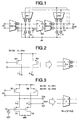
- Fig. 1 shows a circuit configuration explaining a first embodiment of the present invention.
- a low-pass filter consists of two pairs of transconductors Gm1+ (first), Gm1- (second) and Gm2+ (third), Gm2- (fourth), a gain amplifier GA and integrating capacitors.
- Input Vin connects to the positive and negative inputs of transconductor Gm1+.
- Positive output of transconductor Gm1+ connects to the positive output of transconductor Gm1- and the positive input of fixed gain amplifier GA which has a gain coefficient K of 1 and connects to the reference potential node via integrator capacitor C1 and current supply I1 which are connected in parallel.
- the negative output of transconductor Gm1+ connects to the negative output of transconductor Gm1- and the negative input of fixed gain amplifier GA and connects to the reference potential node via integrator capacitor C1 and current supply I2 which are connected in parallel.
- Positive output of fixed gain amplifier GA connects to the positive input of transconductor Gm2+.
- the negative output of fixed gain amplifier GA connects to the negative input of transconductor Gm2+.
- Positive output of transconductor Gm2+ connects to the positive output of transconductor Gm2- and connects to the reference potential node via current supply I3.
- Negative output of transconductor Gm2+ connects to the negative output of transconductor Gm2- and connects to the reference potential node via current supply I4.
- Positive and negative outputs of transconductor Gm2+ connect to both terminals of integrator capacitor C2 and to output Vout.
- the positive output of transconductor Gm2+ connects to the negative inputs of both transconductors Gm1- and Gm2-.
- the negative output of transconductor Gm2+ connects to the positive inputs of both transconductors Gm1- and Gm2-.
- the positive and negative inputs of the transconductors refer to the differential voltage input, and the positive and negative outputs of the transconductors refer to the differential current output.
- the positive and negative inputs of the amplifier refer to the differential voltage input, and the positive and negative outputs refer to the differential voltage output.
- the circuit is a fully differential one, in which all inputs and outputs of transconductors Gm1+, Gm1-, Gm2+ and Gm2- and fixed gain amplifier GA are fully differential signals, and secondly that the number of these building elements on the feedback loop is 3.
- the number of elements is increased to an odd number by inserting a fixed gain amplifier GA with a gain of 1 which does not usually feature in conventional filter topology.
- Each stage consists of two transconductors and an integrating capacitor connected to the output terminals thereof.
- Transconductors Gm1+ and Gm2+ correspond to + input in a single configuration; transconductors Gm1- and Gm2- correspond to - input (feedback input) in a single configuration.
- each transconductor is as follows: Gm1+, Gm1- : gm1 Gm2+, Gm2- : gm2
- Vo VI (gm1gm2) / (C1C2) S+ ⁇ (gm2) / (C2) ⁇ S+ (gm1gm2) / (C1C2)
- each of the transconductors Gm1+, Gm1-, Gm2+ and Gm2- in Fig. 1 has the configuration shown in Fig. 2.
- each transconductor Gm1+, Gm1-, Gm2+ and Gm2- comprises source-coupled differential MOS transistors M1 and M2 whose source is directly connected to power supply, and inputs a differential signal of the previous stage to a gate.
- the drain terminals of these two transconductors are connected each other with the same polarity and integrating capacitors are connected to the positive and negative output terminals which then function as differential output terminals. Both these terminals are biased by the current supply.
- ⁇ electron mobility of the device
- ⁇ ox permittivity of the gate oxide film
- tox gate oxide film thickness
- wafer W is gate width
- L gate length.
- Vb denotes input signal DC voltage corresponding to the power supply voltage
- a transconductor as above which is source-grounded and fully differential solves the problem of second-order distortion liable to occur with a CMOS analog circuit and produces highly linear transconductance. Furthermore, since current supply need not be placed at the differential source connection point, it is possible to used only the voltage portion of the current supply as power voltage, thereby giving the advantage of voltage reduction.
- Fig. 2 shows an example in which PMOS was used in a differential transistor, but exactly the same integrator circuit can be formed when NMOS is used in a differential transistor with the power and the GND reversed, and the same effects can be obtained.
- MOS transistors M3 and M4 are provided as loads for differential MOS transistors M1 and M2 which are the same transistor pair as the transconductor of Fig. 2.
- the previous stage differential signal is input to gates of MOS transistors M1 and M2.
- voltage-to-current conversion properties of differential MOS transistors M1 and M2 are measured under the same conditions as in the calculation above, both M1 and M2 were found to have the same operating properties as was determined in equations (1) and (2) respectively.
- the amplifier is source-ground and has gain roughly equal to the gain for a differential signal but is phase-inverted.
- connection to the next stage determine a phase polarity of the amplifier to output negative-phase, but for a common signal, the amplifier is always phase inverted.
- a common signal is inverted after this amplifier.
- the source of the transconductor shown in Fig. 2 is directly grounded. Since the source is not connected to the current supply for biasing, the common voltage of an input signal cannot be removed. In fact, utilizing this feature eliminates the need for a dedicated DC feedback circuit as shown in the filter circuit in Fig. 1.
- a differential circuit comprising MOS transistors M1 and M2 has high gain between input and output with respect to common voltages because the sources of M1 and M2 are fixed by the power supply. In other words, if input gate voltages both increase, output drain voltages will greatly decrease. Conversely, if input gate voltages both decrease, output drain voltages greatly increase. Moreover, the fixed gain amplifier shown in Fig. 3 has inverse gain with respect to common voltages as already explained.
- I1 and I2 have half the current value of each current supply, these voltages are equal to the VGS value determined by entering these current values into equations (1) and (2).
- this convergence voltage must be predicted beforehand and a common voltage close to that convergence voltage must be given as input Vin. Since each field effect transistor self-biases to a current value determined with the drain side current supply, there is no need to provide a dedicated DC feedback circuit.
- the number of elements in the filter circuit of the present embodiment can be greatly reduced to obtain a low-cost CMOS filter.
- the above example described a filter circuit consisting of two stages, but by adjusting the number of fixed gain amplifiers on the feedback loop, common voltage transmission with negative feedback can be realized in a filter circuit with an increased number of stages.
- This type of common feedback loop is susceptible to voltage oscillation. Since the "Gm2+ ⁇ Gm1- ⁇ 1 ⁇ Gm2+" loop in Fig. 1 has two high-gain stages Gm2+ and Gm1-, phase compensation is essential to prevent oscillation resulting from high-frequency phase delay. In Fig. 1, this is achieved by dividing Gm1 output terminal capacitor C1 into 2 portions and connecting each portion to a corresponding GND. In this way, while 2C1 has a capacitive load with respect to common voltage at the output terminal of transconductor Gm1, there is no capacitive load with respect to common voltage at the output terminal of transconductor Gm2.
- phase compensation in which Gm1 and 2C1 are used to create 1 low-frequency pole can be provided to the common feedback loop. Since the capacitor defines filter characteristics and also provides phase compensation for the common feedback loop, this method has the advantage of being highly economical.
- the second embodiment differs form the first depicted in Fig. 1 in that transconductor Gm1+ is removed, capacitors C1 and C2, which were connected to the reference voltage point, are now connected to input Vin, and transconductors Gm1- (first), Gm2+ (second) and Gm2- (third) are remained.
- Fig. 5 shows a circuit configuration of a third embodiment of the present invention.
- the third embodiment differs from the embodiment shown in Fig. 4 in that input is connected to output Vout via capacitors C2 and C2 and both terminals of capacitor C1 are connected between the input terminals of fixed gain amplifier GA.
- Transconductors Gm-1 (first), Gm2+ (second) and Gm2- (third) are remained.
Landscapes
- Networks Using Active Elements (AREA)
- Amplifiers (AREA)
Applications Claiming Priority (3)
| Application Number | Priority Date | Filing Date | Title |
|---|---|---|---|
| JP33563696A JP3361021B2 (ja) | 1996-12-16 | 1996-12-16 | フィルタ回路 |
| JP335636/96 | 1996-12-16 | ||
| JP33563696 | 1996-12-16 |
Publications (3)
| Publication Number | Publication Date |
|---|---|
| EP0851578A2 true EP0851578A2 (de) | 1998-07-01 |
| EP0851578A3 EP0851578A3 (de) | 2001-09-26 |
| EP0851578B1 EP0851578B1 (de) | 2004-02-25 |
Family
ID=18290821
Family Applications (1)
| Application Number | Title | Priority Date | Filing Date |
|---|---|---|---|
| EP97121978A Expired - Lifetime EP0851578B1 (de) | 1996-12-16 | 1997-12-12 | Filterschaltung |
Country Status (5)
| Country | Link |
|---|---|
| US (1) | US6335655B1 (de) |
| EP (1) | EP0851578B1 (de) |
| JP (1) | JP3361021B2 (de) |
| KR (1) | KR100299740B1 (de) |
| DE (1) | DE69727785T2 (de) |
Families Citing this family (25)
| Publication number | Priority date | Publication date | Assignee | Title |
|---|---|---|---|---|
| JP3482120B2 (ja) * | 1998-03-04 | 2003-12-22 | 株式会社東芝 | 発振回路 |
| US6429720B1 (en) * | 2000-05-12 | 2002-08-06 | Analog Devices, Inc. | RMS-DC converter using a variable gain amplifier to drive a squaring cell |
| US6795843B1 (en) * | 2000-11-08 | 2004-09-21 | Sequoia Communications | Low-distortion differential circuit |
| US6448848B1 (en) * | 2000-12-29 | 2002-09-10 | Intel Corporation | Method of controlling common-mode in differential gm-C circuits |
| KR100869433B1 (ko) * | 2001-01-18 | 2008-11-21 | 엔엑스피 비 브이 | 전자 필터 회로 및 이 회로를 포함하는 반도체 칩 |
| SE521303C2 (sv) * | 2001-12-06 | 2003-10-21 | Ericsson Telefon Ab L M | Differentiellt transistorpar |
| KR20020069181A (ko) * | 2002-05-13 | 2002-08-29 | 주식회사 엠씨링크 | 에프엠 전송신호 발생기용 전압조정 발진기의 집적회로 설계방법 |
| US6600373B1 (en) * | 2002-07-31 | 2003-07-29 | Agere Systems, Inc. | Method and circuit for tuning a transconductance amplifier |
| US20040198287A1 (en) * | 2002-10-08 | 2004-10-07 | Kramer Bradley A. | Simultaneous Gm-C filter and variable gain amplifier circuit |
| JP3976665B2 (ja) * | 2002-11-20 | 2007-09-19 | 富士通株式会社 | バッファ回路装置 |
| DE60217881D1 (de) * | 2002-11-28 | 2007-03-15 | St Microelectronics Srl | Schaltungsvorrichtung zur Herstellung eines nicht-lineares Skaliernetzwerks mit reaktiven Elementen |
| DE10343567B3 (de) * | 2003-09-19 | 2004-11-25 | Infineon Technologies Ag | Mehrstufiger Differenzverstärker |
| US7098718B2 (en) * | 2003-12-11 | 2006-08-29 | The Trustees Of Boston University | Tunable current-mode integrator for low-frequency filters |
| US7098731B1 (en) * | 2004-01-13 | 2006-08-29 | Wyszynski Adam S | Synthesis method for an active polyphase filter |
| EP1689082B1 (de) * | 2005-02-02 | 2008-07-23 | Stmicroelectronics SA | Ein rauscharmes Tiefpassfilter |
| EP1806842B1 (de) * | 2005-12-30 | 2009-09-02 | Stmicroelectronics SA | Schaltkreis eines Transkonduktanzfilters, insbesondere für ein Mobiltelefon |
| US20070194839A1 (en) * | 2006-02-23 | 2007-08-23 | Anadigics, Inc. | Tunable balanced loss compensation in an electronic filter |
| JP4246222B2 (ja) | 2006-07-18 | 2009-04-02 | シャープ株式会社 | キャリア検出回路、それを備えた赤外線信号処理回路、ならびにキャリア検出回路の制御方法 |
| US7626439B2 (en) * | 2006-09-28 | 2009-12-01 | Finisar Corporation | Cross-point adjustment circuit |
| JP4290721B2 (ja) | 2006-11-15 | 2009-07-08 | シャープ株式会社 | バンドパスフィルタ回路、並びに赤外線信号処理回路 |
| JP5423875B2 (ja) * | 2010-03-23 | 2014-02-19 | 富士通株式会社 | 周波数可変フィルタ |
| US9160309B2 (en) * | 2013-12-11 | 2015-10-13 | Qualcomm Incorporated | Area efficient baseband filter |
| US9497049B2 (en) * | 2014-09-04 | 2016-11-15 | Qualcomm Incorporated | Wideband transmitter with high-frequency signal peaking |
| US9369099B1 (en) * | 2014-12-10 | 2016-06-14 | Qualcomm Incorporated | Low power operational transconductance amplifier |
| CN114448384B (zh) * | 2022-02-09 | 2023-07-21 | 深圳市九天睿芯科技有限公司 | 一种滤波电路 |
Family Cites Families (4)
| Publication number | Priority date | Publication date | Assignee | Title |
|---|---|---|---|---|
| US5345190A (en) * | 1993-08-02 | 1994-09-06 | Motorola, Inc. | Modular low voltage filter with common mode feedback |
| JP3318725B2 (ja) * | 1994-01-12 | 2002-08-26 | 株式会社日立製作所 | アナログフィルタ回路 |
| US5625317A (en) * | 1994-08-08 | 1997-04-29 | Texas Instruments Incorporated | Tuning method for integrated continuous-time filters |
| US5528179A (en) * | 1995-05-31 | 1996-06-18 | Texas Instruments Incorporated | Constant capacitance prgrammable transconductance input stage |
-
1996
- 1996-12-16 JP JP33563696A patent/JP3361021B2/ja not_active Expired - Fee Related
-
1997
- 1997-12-12 DE DE69727785T patent/DE69727785T2/de not_active Expired - Fee Related
- 1997-12-12 EP EP97121978A patent/EP0851578B1/de not_active Expired - Lifetime
- 1997-12-16 US US08/991,403 patent/US6335655B1/en not_active Expired - Fee Related
- 1997-12-16 KR KR1019970069057A patent/KR100299740B1/ko not_active IP Right Cessation
Non-Patent Citations (1)
| Title |
|---|
| STEYAERT M ET AL: "A 10.7MHZ CMOS OTA-R-C BANDPASS FILTER WITH 68DB DYNAMIC RANGE AND ON-CHIP AUTOMATIC TUNING" IEEE INTERNATIONAL SOLID STATE CIRCUITS CONFERENCE,US,IEEE INC. NEW YORK, vol. 35, 1 February 1992 (1992-02-01), pages 66-67,245, XP000315424 ISSN: 0193-6530 * |
Also Published As
| Publication number | Publication date |
|---|---|
| EP0851578A3 (de) | 2001-09-26 |
| KR100299740B1 (ko) | 2001-09-03 |
| US6335655B1 (en) | 2002-01-01 |
| KR19980064159A (ko) | 1998-10-07 |
| DE69727785T2 (de) | 2004-12-02 |
| JPH10173482A (ja) | 1998-06-26 |
| JP3361021B2 (ja) | 2003-01-07 |
| EP0851578B1 (de) | 2004-02-25 |
| DE69727785D1 (de) | 2004-04-01 |
Similar Documents
| Publication | Publication Date | Title |
|---|---|---|
| EP0851578B1 (de) | Filterschaltung | |
| JP3318725B2 (ja) | アナログフィルタ回路 | |
| US5345190A (en) | Modular low voltage filter with common mode feedback | |
| Alzaher et al. | A CMOS fully balanced four-terminal floating nullor | |
| Güneş et al. | Design of a high performance mutually coupled circuit | |
| Huang | A MOSFET-only continuous-time bandpass filter | |
| EP1811662B1 (de) | Biquadratisches Tiefpassfilter mit variabler Verstärkung | |
| Chaichana et al. | Current-mode MISO filter using CCCDTAs and grounded capacitors | |
| Lo et al. | A 1 GHz OTA-based low-pass filter with a high-speed automatic tuning scheme | |
| WO2001006648A1 (en) | Integrated circuit | |
| Salama et al. | Parasitic-capacitance-insensitive voltage-mode MOSFET-C filters using differential current voltage conveyor | |
| JP4768186B2 (ja) | 位相補償型インピーダンス変換器 | |
| EP1629594A1 (de) | Verbesserungen an oder bezüglich transkonduktanzschaltungen | |
| EP0696846B1 (de) | Hochpassfilterstruktur mit programmierbaren Nullstellen | |
| Kumngern et al. | Four inputs and one output current-mode multifunction filter using CDTAs and all-grounded passive components | |
| JPH10322143A (ja) | Ac結合回路 | |
| JPH10126214A (ja) | フィルタ回路 | |
| Mehrmanesh et al. | An ultra low-voltage Gm-C filter for video applications | |
| Schaumann et al. | Continuous-time filters | |
| Laber et al. | A 20 MHz 6th order BiCMOS programmable filter using parasitic-insensitive integrators | |
| Zemouri et al. | High frequency Tow-Thomas tunable filter using OTA based voltage op-amp | |
| JP2001339275A (ja) | フィルタ回路とこれを用いた検波回路 | |
| Sanchez-Sinencio et al. | Monolithic programmable state-varable biquadratic OTA-Capacitor (TAC) filters | |
| PANDEY | IMPLEMENTATION AND DESIGN OF ANALOG SIGNAL PROCESSING BY USING OTRA | |
| Minot et al. | BiCMOS OTA for high Q very high frequency continuous-time bandpass filters |
Legal Events
| Date | Code | Title | Description |
|---|---|---|---|
| PUAI | Public reference made under article 153(3) epc to a published international application that has entered the european phase |
Free format text: ORIGINAL CODE: 0009012 |
|
| 17P | Request for examination filed |
Effective date: 19980109 |
|
| AK | Designated contracting states |
Kind code of ref document: A2 Designated state(s): AT BE CH DE DK ES FI FR GB GR IE IT LI LU MC NL PT SE Kind code of ref document: A2 Designated state(s): DE FR GB |
|
| AX | Request for extension of the european patent |
Free format text: AL;LT;LV;MK;RO;SI |
|
| RAP1 | Party data changed (applicant data changed or rights of an application transferred) |
Owner name: KABUSHIKI KAISHA TOSHIBA |
|
| PUAL | Search report despatched |
Free format text: ORIGINAL CODE: 0009013 |
|
| AK | Designated contracting states |
Kind code of ref document: A3 Designated state(s): AT BE CH DE DK ES FI FR GB GR IE IT LI LU MC NL PT SE |
|
| AX | Request for extension of the european patent |
Free format text: AL;LT;LV;MK;RO;SI |
|
| 17Q | First examination report despatched |
Effective date: 20011228 |
|
| AKX | Designation fees paid |
Free format text: DE FR GB |
|
| GRAP | Despatch of communication of intention to grant a patent |
Free format text: ORIGINAL CODE: EPIDOSNIGR1 |
|
| GRAS | Grant fee paid |
Free format text: ORIGINAL CODE: EPIDOSNIGR3 |
|
| GRAA | (expected) grant |
Free format text: ORIGINAL CODE: 0009210 |
|
| AK | Designated contracting states |
Kind code of ref document: B1 Designated state(s): DE FR GB |
|
| REG | Reference to a national code |
Ref country code: GB Ref legal event code: FG4D |
|
| REF | Corresponds to: |
Ref document number: 69727785 Country of ref document: DE Date of ref document: 20040401 Kind code of ref document: P |
|
| ET | Fr: translation filed | ||
| PG25 | Lapsed in a contracting state [announced via postgrant information from national office to epo] |
Ref country code: GB Free format text: LAPSE BECAUSE OF NON-PAYMENT OF DUE FEES Effective date: 20041212 |
|
| PLBE | No opposition filed within time limit |
Free format text: ORIGINAL CODE: 0009261 |
|
| STAA | Information on the status of an ep patent application or granted ep patent |
Free format text: STATUS: NO OPPOSITION FILED WITHIN TIME LIMIT |
|
| 26N | No opposition filed |
Effective date: 20041126 |
|
| GBPC | Gb: european patent ceased through non-payment of renewal fee |
Effective date: 20041212 |
|
| PGFP | Annual fee paid to national office [announced via postgrant information from national office to epo] |
Ref country code: FR Payment date: 20081212 Year of fee payment: 12 |
|
| PGFP | Annual fee paid to national office [announced via postgrant information from national office to epo] |
Ref country code: DE Payment date: 20081205 Year of fee payment: 12 |
|
| REG | Reference to a national code |
Ref country code: FR Ref legal event code: ST Effective date: 20100831 |
|
| PG25 | Lapsed in a contracting state [announced via postgrant information from national office to epo] |
Ref country code: FR Free format text: LAPSE BECAUSE OF NON-PAYMENT OF DUE FEES Effective date: 20091231 |
|
| PG25 | Lapsed in a contracting state [announced via postgrant information from national office to epo] |
Ref country code: DE Free format text: LAPSE BECAUSE OF NON-PAYMENT OF DUE FEES Effective date: 20100701 |