EP0851425B1 - Method and apparatus for using EDO memory devices in a memory system designed for FPM memory devices - Google Patents
Method and apparatus for using EDO memory devices in a memory system designed for FPM memory devices Download PDFInfo
- Publication number
- EP0851425B1 EP0851425B1 EP97310690A EP97310690A EP0851425B1 EP 0851425 B1 EP0851425 B1 EP 0851425B1 EP 97310690 A EP97310690 A EP 97310690A EP 97310690 A EP97310690 A EP 97310690A EP 0851425 B1 EP0851425 B1 EP 0851425B1
- Authority
- EP
- European Patent Office
- Prior art keywords
- memory
- enable input
- extended
- cas
- output enable
- Prior art date
- Legal status (The legal status is an assumption and is not a legal conclusion. Google has not performed a legal analysis and makes no representation as to the accuracy of the status listed.)
- Expired - Lifetime
Links
- 238000000034 method Methods 0.000 title claims description 8
- 239000004020 conductor Substances 0.000 claims description 26
- 230000008878 coupling Effects 0.000 claims description 6
- 238000010168 coupling process Methods 0.000 claims description 6
- 238000005859 coupling reaction Methods 0.000 claims description 6
- 238000005516 engineering process Methods 0.000 description 6
- 230000009977 dual effect Effects 0.000 description 3
- 230000002093 peripheral effect Effects 0.000 description 3
- 239000000872 buffer Substances 0.000 description 2
- 238000010586 diagram Methods 0.000 description 2
- 230000007334 memory performance Effects 0.000 description 2
- 238000012986 modification Methods 0.000 description 2
- 230000004048 modification Effects 0.000 description 2
- 238000004891 communication Methods 0.000 description 1
- 230000007423 decrease Effects 0.000 description 1
- 230000003247 decreasing effect Effects 0.000 description 1
- 238000000802 evaporation-induced self-assembly Methods 0.000 description 1
- 239000011159 matrix material Substances 0.000 description 1
- 230000003068 static effect Effects 0.000 description 1
Images

Classifications
-
- G—PHYSICS
- G11—INFORMATION STORAGE
- G11C—STATIC STORES
- G11C7/00—Arrangements for writing information into, or reading information out from, a digital store
- G11C7/10—Input/output [I/O] data interface arrangements, e.g. I/O data control circuits, I/O data buffers
- G11C7/1015—Read-write modes for single port memories, i.e. having either a random port or a serial port
- G11C7/1018—Serial bit line access mode, e.g. using bit line address shift registers, bit line address counters, bit line burst counters
- G11C7/1021—Page serial bit line access mode, i.e. using an enabled row address stroke pulse with its associated word line address and a sequence of enabled column address stroke pulses each with its associated bit line address
- G11C7/1024—Extended data output [EDO] mode, i.e. keeping output buffer enabled during an extended period of time
Definitions
- the present invention relates generally to the field of memory systems of a computer, and more particularly to a method and apparatus for using EDO memory devices in a memory system designed for FPM memory devices.
- DRAM dynamic random access memory
- a 60 nanosecond (ns) DRAM provides data to a memory controller within. 60ns after assertion of address.
- FPM Fast page mode
- DRAM technology improved memory performance with respect to prior methods by decreasing memory access cycle time.
- FPM memory chips allowed the memory controller to access other data bits in the same "page", or on the same row within the memory matrix of the memory chip.
- Each data bit is accessed by a row and column address, where the row address for FPM is provided set up early to "precharge" a page of the memory chip. Then, a series of column addresses are asserted to access data on the same row. This saves time since the row address does not have to be set up for each column address within that page.
- Extended Data-Out (EDO) memory technology decreases cycle times even further by allowing the memory controller to begin a new column address instruction while it is reading data at the current address.
- the data output drivers for EDO are not turned off when the memory controller removes a column address strobe (CAS) signal to begin the next cycle.
- CAS column address strobe
- the memory controller may negate the CAS signal earlier to prepare for the next cycle, so that each cycle is shorter. This saves approximately 10ns per cycle.
- Memory modules are currently available up to a maximum size of 256 megabytes (MB), which are typically implemented using dual inline memory module (DIMM) configurations for high-end systems, such as workstation PCs and servers.
- DIMM dual inline memory module
- a PC includes up to 16 slots, so that the memory may be extended to a total of 4GB.
- a memory system includes a memory controller that operates in conformity with FPM memory devices to store and retrieve data by providing row and column addresses and corresponding strobe signals including a column address strobe (CAS) signal, and an EDO memory device having an output enable input receiving the CAS signal.
- the memory system includes a memory board coupled through a memory board connector, which receives the CAS signal from the memory controller.
- the memory board includes one or more module connectors, each having an output enable contact receiving the CAS signal. The output enable is not grounded on the memory board, so that it is driven by the CAS signal from the memory controller.
- the EDO memory device is mounted on a memory module and includes an output enable input pin that receives the CAS signal when the memory module is plugged into the memory board. In this manner, the EDO memory device terminates its data output in conjunction with the CAS signal in a similar manner as a comparable FPM memory device. This prevents data corruption and cycle contention during each memory cycle.
- Each memory module connector includes a plurality of conductive contacts including an output enable contact that receives the CAS signal.
- the memory module includes a module connector that plugs into the memory module connector, where the module connector also includes a plurality of conductive contacts including an output enable contact that electrically couples to the output enable contact of the memory module connector.
- the memory module further includes a conductor electrically coupled to the output enable contact of the memory module to receive the CAS signal.
- the EDO memory device is preferably a memory chip having an output enable input pin electrically coupled to the output enable conductor on the memory module.
- each memory module includes a plurality of EDO memory chips, each having an output enable input pin electrically coupled to the output enable conductor on the memory module carrying the CAS signal.
- the EDO memory module has a storage capacity of approximately 256 megabytes (MB).
- the memory system preferably includes a plurality of memory modules, each configured in a similar manner.
- the illustrated embodiment includes up to 16 EDO dual inline memory modules (DIMMs) having a storage capacity of approximately four (4) gigabytes.
- DIMMs EDO dual inline memory modules
- a computer system includes a host bus, a processor that executes memory cycles on the host bus, a memory controller that detects the host bus memory cycles and that operates in conformity with FPM memory devices to store and retrieve data, and a memory system coupled to the memory controller and including EDO memory devices having output enable inputs receiving the CAS signal.
- the memory system may include a memory bus for coupling to a memory board, which includes memory module connectors for receiving compatible memory modules.
- the memory modules include module connectors that plug into any one of the memory module connectors to conduct the CAS signal to the EDO memory devices.
- a method of operating a memory system designed for FPM memory to operate with EDO memory comprises steps of replacing FPM memory devices with EDO memory devices, asserting column and row address signals and corresponding strobe signals including a CAS signal according to FPM operation to the EDO memory devices, and providing the CAS signal to the output enable input of each of the EDO memory devices.
- a method and apparatus according to the present invention allows a user to upgrade a computer system designed for FPM memory with EDO memory.
- the user of a FPM system obtains the benefit of replacing FPM memory modules with EDO memory modules, and thus is able to upgrade to a newer technology without having to maintain an obsolete inventory of FPM devices.
- the computer system 100 is preferably an IBM-compatible, high-end personal computer (PC) system or the like typically used for workstations or server systems.
- the computer system 100 includes a host bus 102 coupled to one or two central processing units (CPUs) CPU1 104 and CPU2 106.
- the CPUs 104, 106 preferably include 32-bit PentiumTM or P6 CPUs by Intel and supporting circuitry.
- the host bus 102 preferably includes 32 address lines and 64 data lines as compatible with the CPUs 104, 106.
- the present invention is illustrated with a multiprocessor, IBM-compatible type PC system, it is understood that the present invention is applicable to other types of computer systems and processors as known to those skilled in the art.
- a memory controller 108 is coupled to the host bus 102 for interfacing a system memory 111 via a memory bus (MB) 109.
- the memory bus 109 includes a plurality of address, data and control signals for interfacing the system memory 111.
- the system memory 111 is preferably implemented with one or more compatible memory modules M1, M2, M3, etc., collectively referred to as M n , plugged into corresponding memory slot connectors C1, C2, C3, etc., collectively referred to as C n , mounted on a removeably coupled memory board 110.
- a memory board connector 109a is mounted on the motherboard and includes contacts for electrically coupling to each of the signals of the memory bus 109.
- the memory board 110 includes a compatible connector 110a for plugging into the memory board connector 109a, where the connector 110a includes corresponding contacts for each of the contacts of the memory board connector 109a, and thus for each of the signals of the memory bus 109.
- the memory board 110 further includes a plurality of conductors (not shown) as known to those skilled in the art for routing each of the contacts of the connector 110a to corresponding contacts of each of the memory slot connectors C n .
- the control signals asserted by the memory controller 108 includes a column address strobe (CAS*) signal for synchronizing the memory cycles of the system memory 111.
- CAS* column address strobe
- An asterisk (*) appended to a signal name denotes negative or inverted logic, where the signal is considered asserted when low.
- the CAS* signal is carried via a corresponding signal line on the memory bus 109, via corresponding contacts of the connectors 109a, 110a, and via a corresponding conductor 110b on the memory board 110 to each of the memory slot connectors C n .
- Another conductor 110c on the memory board 110 carries an output enable signal OE* to each of the memory slot connectors C n .
- the memory bus 109 and the connectors 109a, 1 10a may or may not include lines or contacts for the OE* signal. Either embodiment is contemplated.
- the conductor 110c is coupled to ground through a pull-down resistor (not shown) or the like for pulling the OE* signal low.
- the OE* signal is not pulled low, but is instead coupled to the CAS* signal.
- a conductor 110d is added to electrically couple the conductors 110b and 110c together, so that the OE* signal follows the CAS* signal. The purpose for this will be described more fully below.
- Each of the memory modules M n include a plurality of contacts for electrically coupling to corresponding contacts on any one of the memory slot connectors C n .
- Each of the memory modules M n preferably includes several Extended Data-Out (EDO) dynamic random access memory (DRAM) modules for a total of 256 megabyte (MB) of memory per board.
- EDO Extended Data-Out
- DRAM dynamic random access memory
- the system memory 111 is expandable to a total of 4GB of memory.
- Each of the CPUs 104, 106 are capable of addressing memory and devices mapped between 00000000h and FFFFFFh (4GB of memory space) using a 32-bit address bus.
- the memory controller 108 detects memory cycles on the host bus 102 executed by either of the CPUs 104, 106 for reading data from or writing data to the system memory 111.
- the memory controller 108 executes corresponding memory cycles on the memory bus 109 to retrieve or store data.
- the memory controller 108 converts such host bus memory cycles by retrieving a memory address on the host bus 102 and converting the host address into appropriate row and column addresses suitable for the system memory 111.
- the memory controller 108 also asserts a row address strobe (RAS*) signal and the CAS* signal on the memory bus 109 for synchronizing the memory cycles on the memory bus 109.
- RAS* and CAS* signals or their equivalents are typically inverted for practical memory devices.
- the memory controller 108 is preferably designed for operation with fast page mode (FPM) memory modules, which is typically incompatible with EDO memory operation. As described below, the present invention ensures proper operation between the memory controller 108 and the system memory 111 regardless of whether implemented with FPM or EDO memory.
- FPM fast page mode
- the computer system 100 preferably includes a primary PCI bus 112 coupled to the host bus 102 via a Host-PCI bridge 114.
- the primary PCI bus 112 is typically implemented with one or more PCI slots 116, individually labeled S1, S2, S3, and so on.
- Each of the PCI slots 116 are configured to receive compatible PCI adapter cards incorporating one or more PCI devices as known to those skilled in the art.
- Typical PCI devices include network interface cards (NICs) disk controllers such as a SCSI (small computer systems interface) disk controller, video or graphics controllers, etc.
- NICs network interface cards
- SCSI small computer systems interface
- One or more integrated PCI devices 118 may be integrated onto the motherboard itself and coupled directly to the primary PCI bus 112.
- a secondary PCI bus 120 is provided and coupled to the host bus 102 through another Host-PCI bridge 122.
- the secondary PCI bus 120 is provided for further PCI expansion capability and includes one or more slots 124, which are consecutively numbered above the PCI slots S1-S3, such as PCI slots S4, S5, S6, etc. Although only six (6) PCI slots are shown, more PCI slots may be added to either PCI bus 112, 120 as needed or desired. Additional host PCI buses may be provided on the motherboard and coupled to the host bus 102 as desired.
- the computer system 100 preferably includes an expansion bus 130 coupled to the primary PCI bus 112 through a PCI-Expansion bus bridge 132.
- the expansion bus 130 is any one of many different types, including the industry standard architecture (ISA) bus, also referred to as the AT bus, the extended industry standard architecture (EISA) bus, or the microchannel architecture (MCA) bus, among others.
- ISA industry standard architecture
- EISA extended industry standard architecture
- MCA microchannel architecture
- the expansion bus 130 preferably includes one or more expansion or input/output (I/O) slots 134, individually labeled I1, I2, I3, etc.
- I/O adapter cards may be coupled to the expansion bus 130 through the I/O slots 134, including expansion bus memory, modems, disk controllers, sound cards, NICs and various other types of controllers as known to those skilled in the art.
- the expansion bus 130 also couples to a peripheral expansion bus referred to as the X-bus 140 through a set of bus buffers 142.
- the X-bus 140 is used for connecting various system components and peripherals to the computer system 100, such as a system ROM 144 comprising one or more ROM modules, one or more APICs (advanced programmable interrupt controllers) 146, one or more disk controllers 148 (such as a floppy disk controller (FDC) and a hard disk controller (HDC)), a keyboard controller 150, a real time clock (RTC) and timers 152, communication ports 154, non-volatile static random access memory (NVSRAM) 156, as well as other peripherals not shown, such as a direct memory access (DMA) system, diagnostics ports, command/status registers, battery-backed CMOS memory, etc.
- DMA direct memory access
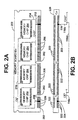
- a side view is shown of a memory module 200, which illustrates any one of the memory modules M n that plug into any one of the memory slot connectors C n to comprise the system memory 111.
- the memory module 200 is implemented as a dual inline memory module (DIMM) configuration, which includes one or more edge connectors 202.
- Each connector 202 includes a plurality of conductive contacts 206 mounted on both sides of each edge connector 202 (opposite side not shown).
- One exemplary embodiment includes three (3) edge connectors 202, a first including 10 contacts 206 on either side, a second including 30 contacts 206 on either side and a third including 44 contacts 206 on either side, for a total of 168 contacts 206.
- Each memory chip 204 is preferably an EDO DRAM module, such as the KM44V16004A or KM44V16104A 16Mx4 bit CMOS DRAM with EDO by Samsung Electronics, or any other similar EDO type memory chip.
- the memory module 200 includes a total of 256 megabyte (MB) of memory, 16 such boards plugged into sixteen of the memory slot connectors C n provides a system memory 111 of 4GB.
- Each of the memory chips 204 includes an inverted output enable pin OE*, which enables or disables the output signals of each memory chip 204 during operation depending upon whether the OE* pin is asserted low or negated high, respectively.
- One of the contacts 206 is an output enable contact 208, which carries the OE* signal from the memory board 110.
- a conductor 210 is electrically coupled to the output enable contact 208 and routed to each output enable pin OE* of each of the memory chips 204.
- Each of the memory chips 204 also includes an inverted CAS* pin.
- Another one of the contacts 206 is a CAS contact 212, which carries the CAS* signal from the memory board 110.
- a conductor 214 is electrically coupled to the CAS contact 212 and routed to each CAS* input pin of each of the memory chips 204.
- the particular location and configuration of contacts, pins and routed conductors shown in Figure 2A is for purposes of illustrating the electrical connections only and not intended to physically duplicate an actual memory module.
- Figure 2B is a top view of a connector 220 for implementing each of the memory slot connectors Cn mounted on the memory board 110 for receiving and connecting to a memory module, such as the memory module 200.
- the connector 220 shown is implemented as a DIMM connector including 84 contacts 222 aligned on two sides a total of 168 contacts 222.
- One of the contacts 222 is an output enable contact 224 connected to the conductor 110c, where the conductor 110c carries the OE* signal from the memory board 110.
- Another one of the contacts 222 is a CAS contact 226 connected to the conductor 110b, where the conductor 110b carries the CAS* signal from the memory controller 108 on the memory bus 109 via the memory board 110.
- the edge connectors 202 of the memory module 200 are aligned with corresponding sections of the connector 220, so that each of the contacts 222 are aligned with and connected to a corresponding one of the contacts 206 of the memory module 200.
- the contacts 224, 226 are electrically connected to the respective contacts 208, 212 for conducting the OE* and CAS* signals from the memory board 110.
- a conductor 110d couples the CAS* and OE* signals, so that the output enable input pins of each of the memory chips 204 follows the CAS* signal from the memory controller 108.
- the memory controller 108 expects that the output signals of FPM memory chips are disabled immediately or very soon after the CAS* signal is negated high during each memory cycle.
- EDO memory chips hold the output data signals valid for a longer period of time after the CAS* signal is negated.
- the memory controller 108 reasserts the CAS* signal low relatively quickly after being negated, which is allowed for FPM operation.
- the memory controller 108 latches the incorrect data resulting in data corruption and cycle contention.
- the CAS* signal is conducted and connected to the output enable OE* signals of each of the memory chips 204 of each of the memory modules M n .
- the OE* output enable pins of each of the memory chips 204 is also pulled high.
- the DRAM output buffers of each of the EDO memory chips 204 of each memory module 200 disable their outputs and terminate the data, thereby eliminating the possibility of cycle contention or data corruption.
- the present invention is illustrated with negative logic CAS* and OE* signal/pins, it is understood that any logic configuration is contemplated for coupling the column address strobe to the output enable signal of EDO memory modules.
- the CAS* and OE* signals may be tied together at any point, including locations on the motherboard (assuming the OE* signal is on the motherboard) or on each of the memory modules M n . However, this would require modification of the motherboard and/or each of the memory modules. It is expedient to disable or remove the pull-down devices coupled to the EO* signal and tie the CAS* and OE* signals together on the memory board which receives the memory modules.
- a method and apparatus for using EDO memory devices in a memory system designed for FPM memory devices enables the use of either FPM or EDO memory modules.
- the EDO memory devices By coupling the column address strobe signal to the output enable inputs of the EDO memory devices, the EDO memory devices operate in a similar manner as FPM memory devices.
- the user of a FPM system obtains the benefits of replacing obsolete FPM memory modules with newer technology EDO memory modules, and unable having to maintain an obsolete inventory of FPM devices.
Landscapes
- Memory System (AREA)
- Dram (AREA)
- Techniques For Improving Reliability Of Storages (AREA)
Applications Claiming Priority (2)
| Application Number | Priority Date | Filing Date | Title |
|---|---|---|---|
| US775315 | 1991-10-11 | ||
| US08/775,315 US6034919A (en) | 1996-12-31 | 1996-12-31 | Method and apparatus for using extended-data output memory devices in a system designed for fast page mode memory devices |
Publications (3)
| Publication Number | Publication Date |
|---|---|
| EP0851425A2 EP0851425A2 (en) | 1998-07-01 |
| EP0851425A3 EP0851425A3 (en) | 1998-12-30 |
| EP0851425B1 true EP0851425B1 (en) | 2003-03-19 |
Family
ID=25104027
Family Applications (1)
| Application Number | Title | Priority Date | Filing Date |
|---|---|---|---|
| EP97310690A Expired - Lifetime EP0851425B1 (en) | 1996-12-31 | 1997-12-31 | Method and apparatus for using EDO memory devices in a memory system designed for FPM memory devices |
Country Status (4)
| Country | Link |
|---|---|
| US (1) | US6034919A (enExample) |
| EP (1) | EP0851425B1 (enExample) |
| JP (1) | JP3930629B2 (enExample) |
| DE (1) | DE69719943T2 (enExample) |
Families Citing this family (3)
| Publication number | Priority date | Publication date | Assignee | Title |
|---|---|---|---|---|
| US7617356B2 (en) * | 2002-12-31 | 2009-11-10 | Intel Corporation | Refresh port for a dynamic memory |
| TWI263899B (en) * | 2004-05-07 | 2006-10-11 | Via Tech Inc | Expandable optical disk recording and playing system and main board thereof |
| CN102955497A (zh) * | 2011-08-18 | 2013-03-06 | 鸿富锦精密工业(深圳)有限公司 | 安装有固态硬盘的主板 |
Family Cites Families (13)
| Publication number | Priority date | Publication date | Assignee | Title |
|---|---|---|---|---|
| US5349566A (en) * | 1993-05-19 | 1994-09-20 | Micron Semiconductor, Inc. | Memory device with pulse circuit for timing data output, and method for outputting data |
| US5457659A (en) * | 1994-07-19 | 1995-10-10 | Micron Technology, Inc. | Programmable dynamic random access memory (DRAM) |
| JP3160477B2 (ja) * | 1994-09-30 | 2001-04-25 | 株式会社東芝 | 半導体メモリ及びそれに用いられるパルス信号発生回路 |
| US5490114A (en) * | 1994-12-22 | 1996-02-06 | International Business Machines Corporation | High performance extended data out |
| US5526320A (en) * | 1994-12-23 | 1996-06-11 | Micron Technology Inc. | Burst EDO memory device |
| US5721859A (en) * | 1994-12-23 | 1998-02-24 | Micron Technology, Inc. | Counter control circuit in a burst memory |
| US6804760B2 (en) * | 1994-12-23 | 2004-10-12 | Micron Technology, Inc. | Method for determining a type of memory present in a system |
| US5682354A (en) * | 1995-11-06 | 1997-10-28 | Micron Technology, Inc. | CAS recognition in burst extended data out DRAM |
| JPH08297965A (ja) * | 1995-04-27 | 1996-11-12 | Mitsubishi Electric Corp | 半導体集積回路装置 |
| US5546344A (en) * | 1995-06-06 | 1996-08-13 | Cirrus Logic, Inc. | Extended data output DRAM interface |
| US5555209A (en) * | 1995-08-02 | 1996-09-10 | Simple Technology, Inc. | Circuit for latching data signals from DRAM memory |
| KR0167687B1 (ko) * | 1995-09-11 | 1999-02-01 | 김광호 | 고속액세스를 위한 데이타 출력패스를 구비하는 반도체 메모리장치 |
| US5644549A (en) * | 1996-03-21 | 1997-07-01 | Act Corporation | Apparatus for accessing an extended data output dynamic random access memory |
-
1996
- 1996-12-31 US US08/775,315 patent/US6034919A/en not_active Expired - Lifetime
-
1997
- 1997-12-31 EP EP97310690A patent/EP0851425B1/en not_active Expired - Lifetime
- 1997-12-31 DE DE69719943T patent/DE69719943T2/de not_active Expired - Fee Related
-
1998
- 1998-01-05 JP JP00015398A patent/JP3930629B2/ja not_active Expired - Lifetime
Also Published As
| Publication number | Publication date |
|---|---|
| DE69719943D1 (de) | 2003-04-24 |
| JPH10228412A (ja) | 1998-08-25 |
| EP0851425A2 (en) | 1998-07-01 |
| JP3930629B2 (ja) | 2007-06-13 |
| US6034919A (en) | 2000-03-07 |
| EP0851425A3 (en) | 1998-12-30 |
| DE69719943T2 (de) | 2003-09-04 |
Similar Documents
| Publication | Publication Date | Title |
|---|---|---|
| US5621902A (en) | Computer system having a bridge between two buses with a direct memory access controller and an alternative memory access controller | |
| US7680968B2 (en) | Switch/network adapter port incorporating shared memory resources selectively accessible by a direct execution logic element and one or more dense logic devices in a fully buffered dual in-line memory module format (FB-DIMM) | |
| US7424552B2 (en) | Switch/network adapter port incorporating shared memory resources selectively accessible by a direct execution logic element and one or more dense logic devices | |
| US5555381A (en) | Microcomputer architecture utilizing an asynchronous bus between microprocessor and industry standard synchronous bus | |
| US5986677A (en) | Accelerated graphics port read transaction merging | |
| US5604871A (en) | Modular host local expansion upgrade | |
| EP0795158B1 (en) | A computer system having a bridge between buses | |
| US5937173A (en) | Dual purpose computer bridge interface for accelerated graphics port or registered peripheral component interconnect devices | |
| US5805833A (en) | Method and apparatus for replicating peripheral device ports in an expansion unit | |
| US5857086A (en) | Apparatus method and system for peripheral component interconnect bus using accelerated graphics port logic circuits | |
| US5923860A (en) | Apparatus, method and system for remote peripheral component interconnect bus using accelerated graphics port logic circuits | |
| US5748945A (en) | Method for slave DMA emulation on a computer system bus | |
| US5301343A (en) | System having microprocessor local memory expansion capability through removable coupling of local memory expansion boards directly to the high speed microprocessor local bus | |
| US6526464B1 (en) | Mechanism to expand address space of a serial bus | |
| EP0851425B1 (en) | Method and apparatus for using EDO memory devices in a memory system designed for FPM memory devices | |
| US5708813A (en) | Programmable interrupt signal router | |
| US6088761A (en) | Reduced pin system interface | |
| JPH11175208A (ja) | 装置をより高電圧の装置から電気的に分離するシステム及び方法 | |
| US5313597A (en) | System for controlling communications among a computer processing unit and a plurality of peripheral devices | |
| US6081861A (en) | PCI migration support of ISA adapters | |
| EP0691616A1 (en) | RAM and ROM control unit | |
| US5740377A (en) | Electronic device for computer | |
| US5307475A (en) | Slave controller utilizing eight least/most significant bits for accessing sixteen bit data words | |
| US5319767A (en) | Slave controller for effecting a block transfer of sixteen bit words between a memory and a data transfer bus | |
| EP0810528B1 (en) | Apparatus for DMA-slave emulation on a computer systems bus |
Legal Events
| Date | Code | Title | Description |
|---|---|---|---|
| PUAI | Public reference made under article 153(3) epc to a published international application that has entered the european phase |
Free format text: ORIGINAL CODE: 0009012 |
|
| AK | Designated contracting states |
Kind code of ref document: A2 Designated state(s): DE FR GB |
|
| AX | Request for extension of the european patent |
Free format text: AL;LT;LV;MK;RO;SI |
|
| PUAL | Search report despatched |
Free format text: ORIGINAL CODE: 0009013 |
|
| AK | Designated contracting states |
Kind code of ref document: A3 Designated state(s): AT BE CH DE DK ES FI FR GB GR IE IT LI LU MC NL PT SE |
|
| AX | Request for extension of the european patent |
Free format text: AL;LT;LV;MK;RO;SI |
|
| 17P | Request for examination filed |
Effective date: 19990621 |
|
| AKX | Designation fees paid |
Free format text: DE FR GB |
|
| GRAG | Despatch of communication of intention to grant |
Free format text: ORIGINAL CODE: EPIDOS AGRA |
|
| 17Q | First examination report despatched |
Effective date: 20020523 |
|
| GRAG | Despatch of communication of intention to grant |
Free format text: ORIGINAL CODE: EPIDOS AGRA |
|
| GRAH | Despatch of communication of intention to grant a patent |
Free format text: ORIGINAL CODE: EPIDOS IGRA |
|
| GRAH | Despatch of communication of intention to grant a patent |
Free format text: ORIGINAL CODE: EPIDOS IGRA |
|
| GRAA | (expected) grant |
Free format text: ORIGINAL CODE: 0009210 |
|
| AK | Designated contracting states |
Designated state(s): DE FR GB |
|
| REG | Reference to a national code |
Ref country code: GB Ref legal event code: FG4D |
|
| REF | Corresponds to: |
Ref document number: 69719943 Country of ref document: DE Date of ref document: 20030424 Kind code of ref document: P |
|
| ET | Fr: translation filed | ||
| PLBE | No opposition filed within time limit |
Free format text: ORIGINAL CODE: 0009261 |
|
| STAA | Information on the status of an ep patent application or granted ep patent |
Free format text: STATUS: NO OPPOSITION FILED WITHIN TIME LIMIT |
|
| 26N | No opposition filed |
Effective date: 20031222 |
|
| PGFP | Annual fee paid to national office [announced via postgrant information from national office to epo] |
Ref country code: GB Payment date: 20071227 Year of fee payment: 11 |
|
| PGFP | Annual fee paid to national office [announced via postgrant information from national office to epo] |
Ref country code: DE Payment date: 20080131 Year of fee payment: 11 |
|
| PGFP | Annual fee paid to national office [announced via postgrant information from national office to epo] |
Ref country code: FR Payment date: 20071217 Year of fee payment: 11 |
|
| GBPC | Gb: european patent ceased through non-payment of renewal fee |
Effective date: 20081231 |
|
| REG | Reference to a national code |
Ref country code: FR Ref legal event code: ST Effective date: 20090831 |
|
| PG25 | Lapsed in a contracting state [announced via postgrant information from national office to epo] |
Ref country code: DE Free format text: LAPSE BECAUSE OF NON-PAYMENT OF DUE FEES Effective date: 20090701 |
|
| PG25 | Lapsed in a contracting state [announced via postgrant information from national office to epo] |
Ref country code: GB Free format text: LAPSE BECAUSE OF NON-PAYMENT OF DUE FEES Effective date: 20081231 |
|
| PG25 | Lapsed in a contracting state [announced via postgrant information from national office to epo] |
Ref country code: FR Free format text: LAPSE BECAUSE OF NON-PAYMENT OF DUE FEES Effective date: 20081231 |