The present invention relates to a high frequency
variable gain amplifier device and a wireless communications
terminal suited to use in, for example, cordless telephones
and portable telephones, etc.
With wireless communications terminals such as, for
example, portable telephones, when the distance to an
opposing station is small, transmission power control is
carried out with respect to the transmission in order to
economize on transmission power usage, prevent saturation of
high frequency amplifiers of an opposing station and reduce
inference with other stations. In particular, in a Code
Division Multiple Access (hereinafter referred to as "CDMA")
method that is one cellular multi-connection method that has
come to the forefront in recent times, highly precise
transmission power control over a wide control band has been
carried out to maintain line capacity.
On the other hand, at a receiver circuit, gain control
is carried out in order to suppress fluctuations in the
level of the received signal due to the influence of changes
in the distance to an opposing station or phasing and to
prevent saturation of the frequency controlled amplifier due
to a high level input signals.
An example will now be described with reference to FIG.
1 of the configuration of a portable telephone taken as an
example of a wireless receiving device.
In FIG. 1, an antenna 11 for transmitting an receiving
signals is connected to an port 12a of an antenna sharing
circuit 12. This antenna sharing circuit 12 is equipped
with transmission side and receiving side ports 12t and 12r,
with bandpass filters (not shown in the drawings of
prescribed characteristics being connected across the
antenna and transmission side ports 12a and 12t and the
antenna side and receiving side ports 12a and 12r.
A high frequency signal from the receiving port 12r of
the antenna sharing circuit 12 is supplied to a mixer 22 via
a low noise high frequency amplifier 21 of a receiver 20. A
local oscillating signal from a local oscillator 23 is
supplied to the mixer 22. The high frequency signal from
the low noise high frequency amplifier 21 is then converted
to an intermediate frequency signal. This intermediate
frequency signal is supplied to a demodulator 25 and a
received power detector 26 via an intermediate frequency
amplifier 24.
The output of the received power detector 26 is
provided as negative feedback to the intermediate frequency
amplifier 24 and the low noise high frequency amplifier 21
so that the gain of these circuits is automatically
controlled. The output of the demodulator 25 is supplied to
a baseband signals processor 31, undergoes prescribed signal
processing, and the received information is played back as
audio signals etc.
The played back received information includes
information indicating the power of the transmission from,
for example, a base station and this indication information
is taken out by a microcomputer 30.
Transmitted information such as audio signals etc. is
subjected to prescribed signal processing at the baseband
signal processor 31 and an output signal of the baseband
signal processor 31 is supplied to a modulator 41 of a
transmitter 40. The output of the modulator 41 is supplied
to a mixer 43 via an intermediate frequency amplifier 42.
A local oscillating signal from the local oscillator 23
is supplied to the mixer 43. The intermediate frequency
signal from the intermediate frequency amplifier 42 is
converted to a high frequency signal and supplied to the
transmission port 12t of the antenna sharing circuit 12 via
a driving amplifier 44 and a high frequency power amplifier
45.
A transmission power control signal from a transmission
power controller 46 is supplied to the intermediate
frequency amplifier 42, driving amplifier 44 and the high
frequency power amplifier 45 so as to control the gain of
these circuits. This transmission power control signal is
generated based on received signal power detection
information from the received power detector 26 and
transmission power indication information from the
microcomputer 30.
In the above, a configuration is described for
transmission power control where control of direct current
power supplied from a power supply to this high frequency
power amplifier is exerted in response to transmission power
control information in such a manner as to raise efficiency
of the high frequency power amplifier at the time of low
transmission output.
On the other hand, with the high frequency amplifier of
this receiving circuit, the configuration also has to be
such that the desired receiving characteristics are also
obtained for high level input signals and the direct current
power supplied from the power supply to this high frequency
amplifier when the input signal is of a low level is
therefore reduced by controlling this power in response to
the level of the received signal.
Portable communication terminals generally continue in
a waiting to receive state for long periods of time. If
savings can be made in the current consumption of the high
frequency amplifier of the receiving side for this period,
substantial savings in the power consumed can be made as
this usage tends to be for long periods even though this
amount is small compared with the amount saved for the high
frequency power amplifier of the transmission side.
With related high frequency variable gain amplifiers,
drain current of either drain is reduced by, for example,
controlling the gate bias voltage or drain bias voltage of
field effect transistors comprising amplifiers in response
to input level (transmission power control information
at the transmission and received signal level at the
receiving circuit) of the amplifiers. The gain of the
amplifiers is therefore made to change and the consumed
power is reduced.
However, in the related technology it is necessary to
adjust the control voltage value and range due to variations
in the semiconductor process. It is therefore difficult to
obtain large gain control widths that are stable.
In order to resolve these problems, in Japanese Patent
Application No. Hei. 7-248697 (applied for on the 31st of
August, 1995) a variable gain amplifier capable of obtaining
a stable large gain control width and capable of achieving
reductions in the power consumed is provided having a
plurality of transmission paths of different gains. One of
these paths are then switched over to and selected by a high
frequency change-over switching and the power supplies for
amplifiers for other transmission paths are turned off.
FIG. 2 shows an example of the variable gain amplifier
disclosed above. At a variable gain amplifier 50 of this
example, there is a transmission path including a high
frequency amplifier 51 of a prescribed gain G51 taking, or
example, field effect transistors (referred to as FETs in
this specification) as active elements and a transmission
path of a through line 52 of a gain of 0dB. These two
transmission paths are switched over between so as to be
selected by high frequency change-over switch circuits 53
and 54. A high frequency signal from the input terminal Ti
is then taken from an output terminal To via one of the
transmission paths in response to the change-over states of
the high frequency change-over switch circuits 53 and 54.
Further, the power supply voltage Vdd of the high
frequency amplifier 51 is supplied via a feed switch 55.
In the example provided, the high frequency change-over
switch circuits 53 and 54 and the feed switch 55 are
controlled so as to be operated together by a controller 60
in response to the transmission power control information or
the received signal level described above. A high frequency
signal is then supplied to the through line 52 and when the
high frequency amplifier 51 is not operating, the feed to
the high frequency amplifier 51 is halted by the feed switch
55 so that unnecessary power consumption by the high
frequency amplifier 51 is avoided.
In this case, the controller 51 control the timing of
the high frequency change-over switch circuits 53, 54 and
the feed switch 55 in such a manner as to avoid the output
terminal To not having a signal. This is because it is not
desirable for output terminal To to have no input when high
frequency change-over switch circuits 53 and 54 are changed
over after first switching over the feed switch 55 to the
side of terminal n when the transmission path of the through
line 52 of a gain of 0 dB is changed over to.
The high frequency change-over switch circuits 53 and
54 in the example in FIG. 2 are each configured of four FETs
of FET Qa to Qd, as shown in FIG. 3. Here, the source and
drains of the first and second FETs Qa and Qb are inserted
in series across a common terminal Tc and the first and
second terminals Ta and Tb, respectively. The source and
drains of the third and fourth FETs Qc and Qd are connected
across the common terminal Tc and ground.
Then, for example, when a d.c. voltage [-Vg] for
control use is supplied to the gates of FETs Qa and Qd and a
d.c. voltage [0]V for control use is supplied to the gates
of FET Qb and FET Qc, the first and third FETs Qa and Qc go
"ON" and the second and fourth FETs Qb and Qd go "OFF" so
that a signal transmission path is formed across the common
terminal Tc and the second terminal Tb.
Further, by making the control voltages supplied to the
gates of each of the FETs Qa to Qd the opposite of that
above, the "ON" and "OFF" states of the FETs Qa to Qd are
inverted and a signal transmission path is formed across the
common terminal Tc and the first terminal Ta.
In the example of FIG. 2, control of the timing of
switching over the high frequency change-over switch
circuits 53, 54 and the feed switch 55 is troublesome.
Further, insertion loss occurs for the high frequency
change-over switch circuits 53 and 54 (Ls53 + Ls54) due to
FET Qa and Qb of one FETs Qa to Qd comprising the high
frequency change-over switch circuits 53 and 54 and there is
therefore the problem that the gain G51 of the high
frequency amplifier 51 is reduced by this portion.
Moreover, as the high frequency change-over switch
circuits 53 and 54 are comprised of four FETs Qa to Qd,
respectively, the scale of the circuit becomes large and the
cost expensive, with this being a particular problem with
regards to the strict demands of compactness at a low price
placed on portable communications terminals.
According to a first aspect of the present invention,
there is provided a high frequency
variable gain amplifier device comprises a transistor
amplifier and a bypass switch. The transistor amplifier is
sypplied with a high frequency signal. The bypass switch is
inserted across an input terminal and an output terminal of
the transistor amplifier and is for controlling forming of a
bypass path. The bypass path is formed by the bypass switch
in accordance with an input of a feed control signal
designating cutting off of a power supply to the transistor
amplifier means. The bypass path is disconnected by the
bypass switch in accordance with an input of a feed control
signal designating feeding of the power supply to the
transistor amplifier.
A feed switch can be included within a power supply
feeding path for feeding a power supply voltage to the
transistor amplifier so that the bypass switch can be
controlled according to an output of the feed switch.
According to a second aspect of the present invention,
there is provided a high frequency variable gain amplifier
device comprises a transistor amplifier, a feed switch, a
bypass switch, a first switch controller and a second switch
controller. The
transistor amplifier is supplied with a high frequency
signal. The feed switch is provided within a power supply
feeding path for the transistor amplifier. The bypass
switch is inserted across an input terminal and an output
terminal of the transistor amplifier and is for controlling
forming of a bypass path. The first switch controller is
for controlling changing oven operation of the feed switch
and the second switch controller is for controlling changing
over operation of the bypass switch. The feed switch and
the bypass switch are controlled by the first and second
switch controllers.
This high frequency variable gain amplifier device can
further comprise matching circuits at the output side of the
transistor amplifier, with a connection point with the
output of the bypass switch being provided within the
matching circuits.
The high frequency variable gain amplifier of the
present invention described above can be provided on a
transmission signal output side or a transmission signal
receiving side of a wireless communications terminal. In
the case of providing the high frequency variable gain
amplifier of the present invention on the transmission
signal receiving side of a wireless communications terminal,
control of the changing over operation of the feed switch
can be carried out in response to the level of a received
signal.
In the present invention, switching between the
transmission path and the bypass path in the transistor
amplifier terminal carried out by on-off operations of both of the
bypass switch provided midway the bypass path and the feed
switch within the power supply feeding path to the transistor
circuit. The bypass switch provided midway the bypass path is
not a select switch as used in the example shown in Fig. 2 and
makes the configuration simple. The transistor amplifier has
only the feed switch that controls the power supply thereto
with neither of its input and output sides being provided with
a switch. As a result, there occurs no insertion loss as in
the example shown in Fig. 2.
Switching is enough carried out only by controlling the
timing in controlling the switching over the bypass switch and
the feed switch. This facilitates the timing control in
controlling the switching.
Embodiments of the present invention can provide a high
frequency variable gain amplifier device and wireless
communications terminal having a scale of circuitry for gain
control use that is small and being of simple construction that
are capable of obtaining a remarkably stable range of gain
control of reducing power consumption.
The following description of embodiments of the present
invention is given merely by way of non-limitative example,
with reference to the accompanying drawings, in which:-
First Embodiment
The following is a description with reference to FIG. 4
to FIG. 8 of the embodiments of a high frequency variable
gain amplifier device of the present invention. Here, an
example is given of the case of a high frequency variable
gain amplifier device that can be applied to the driving
amplifiers 44 and the high frequency power amplifier 45 of
the transmission side or the low noise high frequency
amplifier 21 of the receiving side of the wireless
communication terminal described above in FIG. 1.
The basic configuration of a first embodiment of the
present invention is shown in FIG. 4.
In FIG. 4, a variable gain amplifier 100 comprises a
high frequency amplifier 101 and a high frequency switch
circuit 102 for controlling the switching on and off of the
signal bypass path for this high frequency amplifier 101.
The high frequency amplifier 101 taking, for example,
FETs as active elements is connected across an input
terminal Ti and an output terminal To. high frequency
switch circuit 102 comprising, for example, FETs is then
connected at the middle of a through line 103 connected
across the input and output of the high frequency amplifier
101.
A change-over switch 105 comprising a feed switch that
is comprised of, for example, a plurality of FETs is
connected across a line from which a power supply voltage
Vdd is obtained and a power supply line for the high
frequency amplifier 101. In this case, the side of an input
terminal a of this change-over switch 105 is connected to
the line from which the power supply voltage Vdd is obtained
and the side of an input terminal g of the change-over
switch 105 is connected to earth. The output terminal of
the change-over switch 105 is connected to a change-over
control terminal of the high frequency switch circuit 102.
The change-over switch 105 operates in response to the
aforementioned transmission power control information or
received signal level and is controlled by a feed controller
301.
Under the control of the feed controller 301, as shown
in FIG. 4, when the change-over switch 105 is connected to
the side of input terminal a, the power supply voltage Vdd
is supplied to the high frequency amplifier 101 via the
change-over switch 105 and the high frequency amplifier 101
goes into an operating state.
At the same time, the power supply voltage Vdd passing
through the change-over switch 105 is supplied to the high
frequency switch circuit 102 as a control signal and the
high frequency switch circuit 102 goes off. The connection
across one input terminal Ti and the output terminal To that
passes via the through line 103 is therefore opened.
In this state, the level of the high frequency signal
output occurring at the output terminal To becomes higher
than the level of the inputted high frequency signal
occurring at the input terminal Ti by a gain G101 of the
high frequency amplifier 101.
On the other hand, when the change-over switch 105 is
changed over to a state that is the reverse of that shown in
FIG. 4, the supply of the power supply voltage Vdd is cut,
the operation of the high frequency amplifier 101 is halted,
the earth potential passing through the change-over switch
105 is supplied as a control-signal, the high frequency
switch circuit 102 goes on, and the input terminal Ti and
output terminal To are connected via the through line 103.
In this state, the level of the high frequency output
occurring at the output terminal To is lower than the level
in one high frequency signal input occurring at the input
terminal Ti by a loss Ls that is the sum of the insertion
loss of the high frequency switch circuit 102 and the
mismatching loss occurring at the input terminal Ti.
The gain control width of the variable gain amplifier
100 therefore becomes G101 + |Ls102| due to the changing
over of the change-over switch 105 and the gain G101 of the
terminal frequency amplifier 101 therefore becomes wider.
In this first embodiment, control is exerted so that
the high frequency switch circuit 102 turns the signal
bypass path on and off in response to the changing over to
the change-over switch 105 for feed control use for the high
frequency amplifier 101. Therefore, when functioning of the
high frequency amplifier 101 is halted, the feed to the high
frequency amplifier 101 is halted. Wasteful power
consumption is therefore avoided and gain control range can
be dramatically stabilized.
The high frequency switch circuit 102 of this first
embodiment, as is described in the following, can have a
simple configuration of a single FET or a plurality of FETs
connected in series. The scale and cost can therefore be
substantially received from that of the high frequency
change- over switch circuits 53 and 54 of that previously put
forward shown in FIG. 3.
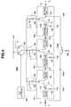
A specific configuration of this first embodiment of
the present invention is shown in FIG. 5. In FIG. 5,
portions corresponding to portions of FIG. 4 are given the
same numerals.
In FIG. 5, a variable gain amplifier 100A comprises
three stages of unit amplifiers 110, 120 and 130 and an FET
102Q taken as a high frequency switch circuit for
controlling the putting on and off of a signal bypass path
for the unit amplifiers 110 to 130.
Capacitors Ci, Ca, Cb and Co and unit amplifiers 110,
120 and 130 are connected alternately on after another.
Each of the unit amplifiers 110, 120 and 130 include FETs
111, 121 and 131, respectively, with the sources of each of
these FETs being connected to earth and each unit amplifier
being of the same configuration.
A high frequency signal from the input terminal Ti is
supplied to the gate of FET 111 of the first unit amplifier
110 via the input side matching circuit 112 and capacitor Ci
and a prescribed gate bias voltage Vgg is supplied via a
resistor 113.
The drain of FET 111 is connected to matching circuit
terminal and change-over switch 105 via a high frequency choke
coil 117 of a drain bias supply circuit 116.
As described above, the side of the input terminal a of
the change-over switch 105 is connected to the line for the
power supply voltage Vdd and the side of the input terminal
g is connected to ground. Change-over is then controlled by
the feed controller 301 in response to transmission power
control information or the level of the received signal.
A high frequency output of the unit amplifier 110 that
is taken via the matching circuit 115 of the output side is
supplied to a unit amplifier 120 of the following stage via
matching capacitor Ca.
In the same way as for the first stage unit amplifier
110, a high frequency signal from the unit amplifier 110 is
supplied to the gate of FET 121 of the unit amplifier 120 of
the following stage via input side matching circuit 122 and
matching capacitor Ca, with a prescribed gate bias voltage
Vgg being supplied via resistor 123.
The drain of FET 121 is connected to a matching circuit
125 and connected to the change-over switch 105 via a high
frequency choke coil 127 of a drain bias supply circuit 126.
A high frequency output of the unit amplifier 120 taken
via matching circuit 125 of the output side is supplied to a
unit amplifier 130 of the final stage via a junction
capacitor Cb.
In the same way as for the unit amplifiers 110 and 120
of the first and following stages, a high frequency signal
from the unit amplifier 120 is supplied to the gate of FET
131 of the final unit amplifier i30 via an input side
matching circuit 132 and junction capacitor Cb, with a
prescribed gate bias voltage Vgg being supplied via a
terminal 133.
The drain of FET 131 is connected to a matching circuit
135 and connected to the change-over switch 105 via a high
frequency choke coil 137 of a drain bias supply circuit 136.
A high frequency output of the unit amplifier 130 from
the matching circuit 135 of the output side is then taken at
the output terminal To via the capacitor Co.
As described above, a depletion type FET 102Q is used
as the high frequency switch circuit 102 of this first
embodiment. The drain of this FET 102Q is connected to the
input terminal Ti via a d.c. blocking capacitor 103c and the
source of this FET 102Q is connected to the drain of the FET
131 of the unit amplifier 130 of the following stage. The
gate of the FET 102Q is connected to ground via resistor
106.
The matching circuits 112 and 115 etc. are given
appropriate publicly known configurations.
Resistors and capacitors (not shown in the drawings)
connected in series are also connected at the drain bias
supply circuit 116 so as to be in parallel with the high
frequency choke coil 117 in order to prevent oscillations.
In FIG. 5, as resistors 113, 123 and 133 are provided
with the purpose of providing isolation, sufficiently large
inductors can also be used. Further, the high frequency
choke coils 117, 127 and 137 can be replaced with a
distributed constant line.
The following is a description of the operation of the
first embodiment of FIG. 5.
When the change-over switch 105 is in the connection
state shown in FIG. 5, drain bias voltages Vdd are supplied
via the drain bias supply circuits 116, 126 and 136 under
the control of the feed controller 301 and the unit
amplifier 110, 120 and 130 enter an operating state.
At the same time, the drain bias voltage Vdd is
supplied to the source of the FET 102Q having its gate
connected to earth and a voltage [-Vdd] is applied across
the gate and source of FET 102Q.
The pinch off voltage Vpf of this FET 102Q is given by:
Vpf > -Vdd
and with the change-over switch 105 in the connection
state shown in the drawings, the drain/source junction of
the FET 102Q is "off" and the connection across the input
terminal Ti and the output terminal To going via the through
lines 103 and 104 becomes open.
In this state, the level of the high frequency signal
of the output occuring at terminal To is higher than the
level of the high frequency signal input occurring at
terminal Ti by the total gain of the unit amplifiers 110,
120 and 130 of G110 + G120 + G130.
On the other hand, when the change-over switch 105 is
changed over to the state opposite to that shown in the
drawings, the supplying of the drain bias voltage Vdd is
interrupted and the operation of the unit amplifiers 110 to
130 is halted.
At the same time, the source of FET 102Q is connected
to ground via the change-over switch 105 and the high
frequency choke coil 137 and a voltage of [0]V is applied
across the gate and source of the FET 102Q. The
drain/source junction of the FET 102Q therefore goes "on"
and the input terminal Ti and output terminal To are
connected via the through lines 103 and 104.
In this state, if the mismatching loss of the side of
the input terminal Ti is ignored, the level of the high
frequency signal of the output occurring at the output
terminal To is lower than the level of the high frequency
signal input occurring at the input terminal Ti by just the
insertion loss Ls of the FET 102Q.
Therefore, by changing over the change-over switch 105,
the gain control width of the variable gain amplifier 100A
becomes G110 + G120 + G130 + |Ls102Q|, which is broader than
the total gain of the unit amplifiers 110, 120 and 130.
As described above, in this embodiment, the FET 102Q
controls the turning on and off of the signal bypassing in
response to the changing over to the change-over switch 105
for control use with respect to the unit amplifiers
110 to 130. Therefore, when the functioning of the unit
amplifiers 110 to 130 is halted, the feed to these unit
amplifiers 110 to 130 is halted. Wasteful consumption of
power is therefore avoided and gain control range can be
dramatically stabilized.
The high frequency switch circuit 102 of this
embodiment can have a simple configuration of a single FET
or a plurality of FETs connected in series. The scale and
cost can therefore be substantially reduced from that of the
high frequency change- over switch circuits 53 and 54 of that
previously put forward shown in FIG. 3.
Further, as the FET 102Q taken as the bypass switch can
be automatically put on and off so as to control changing
over of the change-over switch 105 taken as the feed switch
circuit, the complex change-over timing control of the
switch of the example of FIG. 2 is no longer necessary.
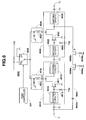
Second Embodiment
Next, a description is given with reference to FIG. 6
and FIG. 7 of a second embodiment of the high frequency
variable gain amplifier device of the present invention
applied to a power amplifier of the aforementioned
transmission circuit.
FIG. 6 shows a configuration of the second embodiment
of the present invention. In FIG. 6, portions corresponding
to those of FIG. 5 are given the same numerals or the same
numerals for the last two digits.
In FIG. 6, a variable gain amplifier 4500 includes unit
amplifiers 4510 and 4520 that provide two stages and two
FETs 4502a and 4502b taken as high frequency switch circuits
for controlling the turning on and off of signal bypassing
to the unit amplifiers 4510 and 4520.
The unit amplifiers 4510 and 4520 include FETs 4511 and
4521, the sources of both of which are connected to earth
and are of the same construction. The unit amplifiers 4510
and 4520 are connected alternately with capacitors Ci, Cc
and Co one after another so as to be inserted across input
terminal Ti and output terminal To.
A high frequency signal from the input terminal Ti is
supplied to the gate of FET 4511 of the first unit amplifier
4510 via an input side matching circuit 4512 and capacitor
Ci and a prescribed gate bias voltage Vgg is supplied via a
resistor 4513.
The drain of FET 4511 is connected to matching circuit
4515 and is connected to change-over switch 4505 via a high
frequenzy choke coil 4517 of a drain bias supply circuit
4516.
As for the previous embodiment, the side of an input
terminal a of this change-over switch 4505 is connected to
one power supply voltage line Vdd and the side of the input
terminal g is connected to earth. Change-over control is
then carried out by the feed controller 301 in response to
the transmission power control information described
previously.
A high frequency output of the unit amplifier 4510
taken via the matching circuit 4515 on the side of the
output is supplied to the following stage unit amplifier
4520 via a junction capacitor Cc.
In the same way as for the unit amplifier 4510 of the
first stage, a high frequency signal from the unit amplifier
4510 is supplied to the gate of FET 4521 of the unit
amplifier 4520 of the following stage via a matching circuit
4522 and capacitor Cc of the input side, with a prescribed
gate bias voltage Vgg being supplied via a resistor 4523.
The drain of FET 4521 is connected to a matching
circuit 4525 and is connected to change-over switch 4505 via
a high frequency choke coil 4527 of a drain bias supply
circuit 4526.
A high frequency output of the unit amplifier 4520
taken via the matching circuit 4525 of the output side is
taken from the output terminal To via the capacitor Co.
In the second embodiment of FIG. 6, with the two
dispersion type FETs 4502a and 4502b taken as the high
frequency bypass switch circuit, the source of FET 4502a and
the drain of FET 4502b are connected in series and these
transistors are then inserted in the middle of a through
line 4503.
The drain of FET 4502a is then connected to the input
terminal Ti via a d.c. blocking capacitor 4503c and the
source of FET 4502b is connected to the drain of FET 4521 of
the unit amplifier 4520. The gates of FET 4502a and 4502b
are connected to ground via resistor 4506a and 4506b.
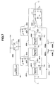
Various configurations can be adopted for the matching
circuit 4525 for the output side of the unit amplifier 4520
of the final stage depending on the operating frequency and
use etc., an example of which is shown in FIG. 7. In the
example in FIG. 7, it is possible to provide a point of
connection with the source of the FET 4502b at the matching
circuit 4525 when the potential is equal to the drain
potential.
By providing a connection point within the matching
circuit 4525 in this way, it is possible to adjust the
impedance viewed from the output terminal To when the FETs
4502a and 4502b of the frequency switch circuit are on. By
then making adjustments to the most suitable impedance,
fluctuations in the characteristics of circuits connected to
the output terminal To due to load fluctuations can be
suppressed.
In addition to describing the detailed configuration of
one matching circuit 4525, FIG. 7 is exactly the same as
FIG. 6 and the description of the remaining portions is
therefore omitted.
Next, the operation of the second embodiment of FIG. 6
is described.
When the transmission output is made high based on the
aforementioned transmission power control information, the
change-over switch 4505 is put to the connection state shown
in the drawings under the control of the feed controller
301, the drain bias voltage Vdd is supplied via the drain
bias supply circuits 4516 and 4526 and both of the unit
amplifiers 4510 and 4520 are put into operating states.
At the same time, the drain bias voltage Vdd of the
unit amplifier 4520 is supplied to the source of FET 4502b,
the gate of which is connected to earth. A voltage [-Vdd]
is then applied across the gate/emitter of the FET 4502b.
The pinch off voltage Vpf of this FET 4502b is given
by:
Vpf > -Vdd
and with the change-over switch 4505 connected in the
state shown in the drawings the drain source junction of the
FET 4502b goes "off", the drain source function of the FET
4502a connected in series with this also goes "off", and the
connection that goes across the input terminal Ti and the
output terminal To via the d.c. blocking capacitor 4503c and
the through line 4503 is opened.
In this state, the level of the high frequency signal
output occurring at the terminal To is higher than the level
of the high frequency signal input occurring at the input
terminal Ti by just the gain G4520 + G4520(dB) of both the
unit amplifiers 4510 and 4520.
On the other hand, when the transmission output is
lowered, the change-over switch 4505 is changed over to the
opposite of the state shown in the drawings, supplying of
the drain bias voltage Vdd is cut and the operation of both
of the unit amplifiers 4510 and 4520 is halted.
At the same time, the source of the FET 4502b is
connected to earth via the change-over switch 4505 and the
high frequency choke coil 4527. The drain/source junction
of the FET 4502b is then made to go "on" by applying a
voltage of [0]V across the gate and source of this FET
4502b.
Together with this, the drain/source junction of the
FET 4502b also goes on as a result of also applying a
voltage of [0]V across the gate and drain of FET 4502a and a
connection is made across the input terminal Ti and the
output terminal To via the through lines 4503 and 4504.
In this state, if the mismatching loss of the side of
the input terminal Ti is ignored, the level of the high
frequency signal output occurring at the output terminal To
is lower than the level of the high frequency signal input
occuring at the terminal Ti by just the insertion loss Ls
4502a + Ls 4502b of FET 4502a and FET 4502b.
Therefore, by changing over the change-over switch
4505, the gain control width of the variable gain amplifier
4500 becomes G4510 + F4520 + |Ls4502a + Ls4502b|, with this
being wider than the total gain G4510 + G4520 of the unit
amplifiers 4510 and 4520.
For example, a total gain of 25 dB is obtained in the
case of a two stage unit amplifier at a frequency band of 2
GHz. Further, the loss for the signal path going via the
two switch FETs of an "on" state is about 3 dB including
mismatching loss at the input side.
As described above, in this second embodiment, FET
4502a and FET 4502b control the turning on and off of the
signal bypass in response to the change-over of the change-over
switch 4505 for feed control with respect to the unit
amplifiers 4510 and 4520. Therefore, when the functioning
of the unit amplifiers 4510 and 4520 is halted, feeding to
these unit amplifiers 4510 and 4520 is halted. Unnecessary
power consumption is therefore avoided and a much more
stable gain control width is obtained.
In particular, as the handling power of the power
amplifier of the transmission is large, power consumption
can be reduced in an effective manner.
Further, the switch of this embodiment can have a
simple configuration of the two FETs 4502a and 4502b
connected in series. The scale and cost can therefore be
substantially reduced from that of the high frequency
change- over switch circuits 53 and 54 of that previously put
forward shown in FIG. 3.
The high frequency switch of this embodiment is
therefore two FETs 4502a and 4502b connected in series and
the isolation of this switch when in an "off" state can
therefore be made large.
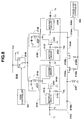
Third Embodiment
A description will be given with reference to FIG. 8 of
a third embodiment of the high frequency variable gain
amplifier device of the present invention applied to an
initial stage of an amplifier of a receiving device.
FIG. 8 shows a configuration of the third embodiment of
the present invention. In FIG. 8, portions corresponding to
those of FIG. 5 are given the same numerals or the last two
digits are made to be the same.
In FIG. 8, a variable gain amplifier 2100 includes two
stages of unit amplifiers 2110 and 2120, and two FETs 2102a
and 2102b taken as the high frequency bias switch for
controlling the turning on and off of a through line 2103 as
a signal bypass path with respect to these unit amplifiers
2110 and 2120.
The unit amplifiers 2110 and 2120 include FETs 2111 and
2121, the sources of both of which are connected to earth
and are of the same construction. The unit amplifiers 2110
and 2120 are connected alternately with capacitors Ci, Cc
and Co one after another so as to be inserted across input
terminal Ti and output terminal To.
A high frequency signal from the input terminal Ti is
supplied to the gate of FET 2111 of the first unit amplifier
2110 via an input side matching circuit 2112 and capacitor
Ci and a prescribed gate bias voltage Vgg is supplied via a
resistor 2113.
The drain of FET 2111 is connected to matching circuit
2115 and is connected to change-over switch 2105 via a high
frequency choke coil 2117 of a drain bias supply circuit
2116.
As for the previous embodiments, the side of an input
terminal a of this change-over switch 2105 is connected to
the power supply voltage line Vdd and the side of the input
terminal g is connected to earth. Change-over control is
then carried out by the feed controller 301 in response to
the transmission power control information describes previously.
A high frequency output of the unit amplifier 2110
taken via the matching circuit 2115 on the side of the
output is supplied to the following stage unit amplifier
2120 via a junction capacitor Cc.
In the same way as for the unit amplifier 2110 of the
first stage, a high frequency signal from the unit amplifier
2110 is supplied to the gate of FET 2121 of the unit
amplifier 2120 of the following stage via a matching circuit
2122 and capacitor Cc of the input side, with a prescribed
gate bias voltage Vgg being supplied via a resistor 2123.
The drain of FET 2121 is connected to a matching
circuit 2125 and is connected to chance-over switch 2105 via
a high frequency choke coil 2127 of a drain bias supply
circuit 2126.
A high frequency output of the unit amplifier 2120
taken via the matching circuit 2125 of the output side is
taken from the output terminal To via the capacitor Co.
In this third embodiment, as with the embodiment of
FIG. 6, with the two dispersion type FETs 2102a and 2102b
taken as the high frequency bypass switch circuit, the
source of FET 2102a and the drain of FET 2102b are connected
together so as to be used in series.
In the third embodiment of FIG. 8, the source of FET
2102a is connected to the input terminal Ti via a d.c.
blocking capacitor 2103c and connected to ground via a high
frequency choke coil 2107. The drain of the remaining FET
2102b is then connected to the drain of the final stage unit
amplifier 2120 via a d.c. blocking capacitor 2104c.
Further, in the third embodiment of FIG. 8, a
prescribed control signal S302 from a change-over controller
302 is supplied to the gates of FET 2102a and FED 2102b that
are in parallel via resistors 2106a and 2106b in response to
the aforementioned received level.
By using the above configuration, with the third
embodiment of FIG. 8 as for the second embodiment of FIG. 6,
the connection end of the source of FET 2102a is by no means
limited to portions supplied with the drain bias voltage Vdd
such as, for example, the unit amplifier 2120 and can be
selected within an appropriate scope. Further, the FETs
2102a and 2102b are by no means limited to the depression
type of the case described in FIG. 6 and operation is also
possible with an enhancement type.
The following is a description of the operation of the
third embodiment of FIG. 8.
In this third embodiment, when the level of the
received signal is low, the change-over switch 2105 goes
into the connection state shown in the drawings under the
control of the feed controller 301 and the d.c. level of the
control signal S302 from the change-over controller 302
becomes lower [Vgg] than the pinch off voltage Vpf of the
FET 2102a and FET 2102b.
Both of the unit amplifiers 2110 and 2120 are then
supplied with the drain bias voltage Vdd via the change-over
switch 2105 and the drain bias supply circuits 2115 and 2126
and therefore enter operating states.
The drain/source junction of the FET 2102a then goes
"off", the drain/source function of the FET 2102b connected
in parallel with FET 2102a also goes off, and the connection
across the input terminal Ti and the output terminal To via
the d.c. blocking capacitor 2103c, through lines 2103 and
2104 and the the d.c. blocking capacitor 2104c is then made to
be open.
In this state, the level of the high frequency signal
output occuring at the output terminal To is higher than
the level of the high frequency signal input occurring at
the input terminal Ti by the gains G2110 + G2120 of both of
the unit amplifiers 2110 and 2120.
On the other hand, when the level of the received
signal is high, the change-over switch 2105 is changed over
to the state that is the opposite of the state shown in the
drawings and the d.c. level of the control signal S302 from
the change-over controller 302 is changed over to the ground
potential.
The supplying of the drain bias voltages is then shut
off and both of the unit amplifiers 2110 and 2120 cease operation.
Further, the gate and sources become of the same
potential to allow the "on" state between the drain and the
source of the FET 2102a. In accompaniment with this, the
gate and source of the FET 2102b connected in series with
this FET become of the same potential to allow also the "on"
state between the drain and the source of the FET 2102b.
The input terminal Ti and the output terminal To are
therefore connected via the d.c. blocking capacitor 2103c,
through lines 2103 and 2104 and the d.c. blocking capacitor
2104c.
In this state, if the mismatching loss on the side of
the input terminal Ti is ignored, the level of the high
frequency signal output occurring at the terminal To is
lower than the level of the high frequency signal input
occurring at the terminal Ti by just the insertion loss
Ls2102a + Ls2102b of the FET 2102a and the FET 2102b.
The gain control range of the variable gain amplifier
2100 due to the switching of the change-over switch 205
becomes G2110 + G2120 + |Ls2102a + Ls2102b|, which is wider
than the total gain G2110 + G2120 of the unit amplifiers
4510 and 4520.
As described above, FET 2102a and FET 2102b control the
turning on and off of the signal bypass in response to
change-over of the change-over switch 2105 for feed control
use with respect to the unit amplifiers 2110 and 2120 under
the control of the feed controller 301 and the change-over
controller 302. When the functioning of the unit amplifiers
2110 and 2120 is halted, feeding to the unit amplifiers 2110
and 2120 is halted so that wasteful consumption of power is
avoided and a markedly more stable gain control range is
obtained.
The high frequency switch of this third embodiment has
a simple configuration of the two FETs 2102a and 2102b
connected in series. The scale and cost can therefore be
substantially reduced from that of the high frequency
change- over switch circuits 53 and 54 of that previously put
forward shown in FIG. 3.
The high frequency switch of this third embodiment is
therefore two FETs 2102a and 2102b connected in series and
the isolation when in an "off" state can therefore be made
sufficient.
In each of the above embodiments, FETs are used as both
the active elements of the amplifiers and are used in the
high frequency switch but the present invention is by no
means limited in this respect and bipolar transistors can
also be used.
As described above, according to the present invention,
a stable gain control range can be obtained for each stage
using a simple configuration; power consumption can be
reduced and the scale of circuitry used in gain control can
be reduced.
Control of the timing of the changing over of the feed
switch and the bias switch is therefore no longer necessary
and ccncrol is easier as a result.