EP0845659B1 - Abtastelement für eine Positionsmesseinrichtung - Google Patents
Abtastelement für eine Positionsmesseinrichtung Download PDFInfo
- Publication number
- EP0845659B1 EP0845659B1 EP97120515A EP97120515A EP0845659B1 EP 0845659 B1 EP0845659 B1 EP 0845659B1 EP 97120515 A EP97120515 A EP 97120515A EP 97120515 A EP97120515 A EP 97120515A EP 0845659 B1 EP0845659 B1 EP 0845659B1
- Authority
- EP
- European Patent Office
- Prior art keywords
- scanning
- tracks
- graduation
- track
- conductor
- Prior art date
- Legal status (The legal status is an assumption and is not a legal conclusion. Google has not performed a legal analysis and makes no representation as to the accuracy of the status listed.)
- Expired - Lifetime
Links
- 238000004804 winding Methods 0.000 claims abstract description 20
- 230000005672 electromagnetic field Effects 0.000 claims abstract description 11
- 230000001939 inductive effect Effects 0.000 claims abstract description 9
- 230000001419 dependent effect Effects 0.000 claims abstract description 6
- 230000000737 periodic effect Effects 0.000 claims abstract description 4
- 239000004020 conductor Substances 0.000 claims description 43
- 230000005284 excitation Effects 0.000 claims description 31
- NCGICGYLBXGBGN-UHFFFAOYSA-N 3-morpholin-4-yl-1-oxa-3-azonia-2-azanidacyclopent-3-en-5-imine;hydrochloride Chemical compound Cl.[N-]1OC(=N)C=[N+]1N1CCOCC1 NCGICGYLBXGBGN-UHFFFAOYSA-N 0.000 claims description 4
- 238000010276 construction Methods 0.000 claims description 2
- 238000006073 displacement reaction Methods 0.000 claims description 2
- 101100367244 Arabidopsis thaliana SWA1 gene Proteins 0.000 abstract 1
- 101150098716 SWA2 gene Proteins 0.000 abstract 1
- 239000000463 material Substances 0.000 description 6
- 238000005516 engineering process Methods 0.000 description 3
- 230000007613 environmental effect Effects 0.000 description 3
- 238000011156 evaluation Methods 0.000 description 3
- 238000000034 method Methods 0.000 description 3
- 239000004593 Epoxy Substances 0.000 description 2
- 230000015572 biosynthetic process Effects 0.000 description 2
- 238000001514 detection method Methods 0.000 description 2
- 238000004519 manufacturing process Methods 0.000 description 2
- 238000005259 measurement Methods 0.000 description 2
- RYGMFSIKBFXOCR-UHFFFAOYSA-N Copper Chemical compound [Cu] RYGMFSIKBFXOCR-UHFFFAOYSA-N 0.000 description 1
- 229910052802 copper Inorganic materials 0.000 description 1
- 239000010949 copper Substances 0.000 description 1
- 238000000605 extraction Methods 0.000 description 1
- 230000003287 optical effect Effects 0.000 description 1
Images

Classifications
-
- G—PHYSICS
- G01—MEASURING; TESTING
- G01D—MEASURING NOT SPECIALLY ADAPTED FOR A SPECIFIC VARIABLE; ARRANGEMENTS FOR MEASURING TWO OR MORE VARIABLES NOT COVERED IN A SINGLE OTHER SUBCLASS; TARIFF METERING APPARATUS; MEASURING OR TESTING NOT OTHERWISE PROVIDED FOR
- G01D5/00—Mechanical means for transferring the output of a sensing member; Means for converting the output of a sensing member to another variable where the form or nature of the sensing member does not constrain the means for converting; Transducers not specially adapted for a specific variable
- G01D5/12—Mechanical means for transferring the output of a sensing member; Means for converting the output of a sensing member to another variable where the form or nature of the sensing member does not constrain the means for converting; Transducers not specially adapted for a specific variable using electric or magnetic means
- G01D5/14—Mechanical means for transferring the output of a sensing member; Means for converting the output of a sensing member to another variable where the form or nature of the sensing member does not constrain the means for converting; Transducers not specially adapted for a specific variable using electric or magnetic means influencing the magnitude of a current or voltage
- G01D5/20—Mechanical means for transferring the output of a sensing member; Means for converting the output of a sensing member to another variable where the form or nature of the sensing member does not constrain the means for converting; Transducers not specially adapted for a specific variable using electric or magnetic means influencing the magnitude of a current or voltage by varying inductance, e.g. by a movable armature
- G01D5/204—Mechanical means for transferring the output of a sensing member; Means for converting the output of a sensing member to another variable where the form or nature of the sensing member does not constrain the means for converting; Transducers not specially adapted for a specific variable using electric or magnetic means influencing the magnitude of a current or voltage by varying inductance, e.g. by a movable armature by influencing the mutual induction between two or more coils
- G01D5/2053—Mechanical means for transferring the output of a sensing member; Means for converting the output of a sensing member to another variable where the form or nature of the sensing member does not constrain the means for converting; Transducers not specially adapted for a specific variable using electric or magnetic means influencing the magnitude of a current or voltage by varying inductance, e.g. by a movable armature by influencing the mutual induction between two or more coils by a movable non-ferromagnetic conductive element
-
- G—PHYSICS
- G01—MEASURING; TESTING
- G01D—MEASURING NOT SPECIALLY ADAPTED FOR A SPECIFIC VARIABLE; ARRANGEMENTS FOR MEASURING TWO OR MORE VARIABLES NOT COVERED IN A SINGLE OTHER SUBCLASS; TARIFF METERING APPARATUS; MEASURING OR TESTING NOT OTHERWISE PROVIDED FOR
- G01D5/00—Mechanical means for transferring the output of a sensing member; Means for converting the output of a sensing member to another variable where the form or nature of the sensing member does not constrain the means for converting; Transducers not specially adapted for a specific variable
- G01D5/12—Mechanical means for transferring the output of a sensing member; Means for converting the output of a sensing member to another variable where the form or nature of the sensing member does not constrain the means for converting; Transducers not specially adapted for a specific variable using electric or magnetic means
- G01D5/14—Mechanical means for transferring the output of a sensing member; Means for converting the output of a sensing member to another variable where the form or nature of the sensing member does not constrain the means for converting; Transducers not specially adapted for a specific variable using electric or magnetic means influencing the magnitude of a current or voltage
- G01D5/20—Mechanical means for transferring the output of a sensing member; Means for converting the output of a sensing member to another variable where the form or nature of the sensing member does not constrain the means for converting; Transducers not specially adapted for a specific variable using electric or magnetic means influencing the magnitude of a current or voltage by varying inductance, e.g. by a movable armature
- G01D5/204—Mechanical means for transferring the output of a sensing member; Means for converting the output of a sensing member to another variable where the form or nature of the sensing member does not constrain the means for converting; Transducers not specially adapted for a specific variable using electric or magnetic means influencing the magnitude of a current or voltage by varying inductance, e.g. by a movable armature by influencing the mutual induction between two or more coils
- G01D5/2046—Mechanical means for transferring the output of a sensing member; Means for converting the output of a sensing member to another variable where the form or nature of the sensing member does not constrain the means for converting; Transducers not specially adapted for a specific variable using electric or magnetic means influencing the magnitude of a current or voltage by varying inductance, e.g. by a movable armature by influencing the mutual induction between two or more coils by a movable ferromagnetic element, e.g. a core
Definitions
- the present invention relates to a scanning element for a position measuring device according to the preamble of claim 1.
- position measuring devices in which position-dependent extraction Information a periodic measurement division is optically scanned
- measuring systems which are based on alternative scanning principles. Such position measuring devices prove to be particularly useful under certain Environmental conditions as less susceptible than those mentioned optical measuring systems.
- Corresponding environmental conditions are, for example given in applications where the rotational movement of the Shaft of a drive is to be detected.
- a position measuring device the can also be used under harsher environmental conditions described for example in EP 0 289 033 B1.
- the corresponding sensing element for this purpose includes one or more excitation coils in the area the scanned division track a homogeneous electromagnetic field produce.
- sensor windings are provided on the scanning side are also arranged in the homogeneous field of the excitation coils and for Detection of the electromagnetic induced in the conductive areas Fields are used so that an output signal modulated as a function of displacement results. In this way, the relative movement can be between the graduation track and the scanning element.
- a position measuring device is also refer to EP 0 182 085.
- a similarly constructed inductive position measuring device is also known from DE 195 04 307. Among other things, it also proposes not just scanning a single division track, but rather more To provide traces that are read in the manner described can be. Details regarding the specific design of a measuring arrangement with several scanned graduation tracks and options for the generation of the excitation fields are not specified in this document.
- the object of the present invention is therefore a generic scanning element for an inductive position measuring device that even in the case of several provided scanning tracks a reliable one Functioning is ensured.
- this should also apply to several Tracing the generation of homogeneous excitation fields in the area of the different Traces of scanning can be guaranteed.
- Subject of claim 11 is further a position measuring device, in which a scanning element designed according to the invention is used becomes.
- the measures according to the invention now ensure that the sensor windings of all the provided scanning tracks are arranged in a homogeneous electromagnetic field even in the case of a plurality of scanning tracks arranged adjacent to one another.
- the appropriate connection of the excitation elements makes it possible in a simple manner to generate a homogeneous excitation field in the area of the various scanning tracks.
- Different scanning tracks can be provided for a wide variety of purposes, such as using one scanning track for drive commutation, another for incremental position determination, etc.
- the formation of the excitation elements in the form of conductor track units, consisting of several parallel, current-carrying individual conductor tracks, has proven to be advantageous.
- the scanning element according to the invention can be flexibly adapted to different measurement requirements.
- the measures according to the invention can also be used both in linear and in rotary position measuring devices; it can also be used in a wide variety of measuring systems, ie both in absolute and incremental measuring systems of various types and in corresponding combinations thereof. Further advantages and details of the scanning element according to the invention result from the following description of an exemplary embodiment with reference to the attached figures.
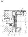
- FIG. 1 shows a sectional side view of an embodiment of an inductive position measuring device in which a scanning element designed according to the invention is used.
- the position measuring device shown here is designed as an angle measuring device that serves to detect the angle of rotation of the shaft 1 of a drive relative to a stationary drive part 2.
- Reference number R in FIG. 1 denotes the axis of rotation of shaft 1; further drive details are not shown.
- a partial disk 3 is fastened to the shaft 1 of the drive and is scanned with the aid of the stationary scanning element 5 designed according to the invention.
- the graduated disk 3 rotating with the shaft 1 about the axis of rotation R consists of a graduation carrier 3.1 on which two radially adjacent graduation tracks are arranged.
- the scanning element 5 is fastened in the housing or stationary part 2 of the drive 2 to a mounting element 6 by means of a screw 9.
- an evaluation and supply unit arranged downstream of the scanning element 5. This serves on the one hand to supply the scanning element 5 or the excitation elements arranged thereon with a supply voltage and on the other hand to evaluate the periodically modulated, position-dependent output signals of the scanning element 5 which result from the scanning of the indexing disk 3.
- Such an evaluation and supply unit can be implemented, for example, in the form of a numerical control.
- a position measuring system with a stationary partial disk and rotating scanning unit can of course also be implemented on the basis of the considerations according to the invention.
- EP 0 182 085 B1 already mentioned at the beginning.
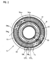
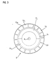
- FIG. 2 shows a front view of the scanning element 5; the partial disk 3 thus scanned is also shown in FIG. 3 in a front view.
- the two graduation tracks T1, T2 are circular and are arranged radially adjacent on a graduation carrier 3.1.
- epoxy material serves as the material for the division carrier 3.1.
- the two graduation tracks T1, T2 each consist of a periodic sequence of alternately arranged electrically conductive graduation areas T1 L , T2 L and non-conductive graduation areas T1 N , T2 N. Copper, for example, has been found to be a suitable material for the electrically conductive partial areas T1 L , T2 L , which is applied to the graduation carrier 3.1. In contrast, in the non-conductive graduation areas T1 L , T2 L , the graduation carrier 3.1 was merely not coated and is identical to the material of the graduation carrier 3.1. In the embodiment shown, the inner graduation track T1 only consists of a first semicircular graduation area T1 L with electrically conductive material and a second semicircular graduation area T1 N , in which no conductive material is arranged. The scanning of the graduation track T1 with the aid of the scanning element 5 explained below results in a relatively coarse, absolute position information within one revolution of the indexing disk 3 about the axis of rotation R.
- a second graduation track T2 is arranged on the graduation carrier 3.1, which consists of a plurality of electrically conductive graduation areas T2 L and graduation areas T2 N arranged between them.
- the different graduation areas T2 L , T2 N are formed just like the graduation area T1 L of the first graduation track T1.
- the second graduation track T2 in the exemplary embodiment shown comprises 16 periodically arranged, electrically conductive graduation areas T2 L and correspondingly 16 non-conductive graduation areas T2 N arranged therebetween.
- the length of the electrically conductive graduation areas T2 L in the measuring direction is more than 10 times greater than the corresponding length of the non-conductive graduation areas T2 N , ie a ratio of the lengths of the different graduation areas in this graduation track that differs from 1: 1 is preferably selected.
- the result of the scanning of the second graduation track T2 is therefore a resulting incremental signal during the relative movement of indexing disk 3 and scanning element 5.
- a high-resolution rotation angle determination is possible via such an arrangement.
- the scanning element 5 according to the invention, shown in FIG. 2 and intended for scanning the indexing disk 3, comprises two scanning tracks A1, A2 assigned to the graduation tracks T1, T2, which are also circular and are arranged radially adjacent on a carrier element 10.
- a single carrier element 10 is referred to below, although in the embodiment of the scanning element 5 shown a multi-layer structure of the same is provided with a plurality of printed circuit board layers, connecting layers and sensor layers. With regard to this multilayer structure, reference is made to the description of FIG. 6.
- the scanning track A1 assigned to the inner or absolute graduation track T1 consists of a total of two flat sensor windings SW A1 and SW B1 , each of which delivers a single signal period during the scanning over the circumference of the scanning track A1.
- the two sensor windings SW A1 and SW B1 are here offset relative to one another on the carrier element 10 of the scanning element 5, so that on the output side when scanning the rotating part disk 3, two output signals SIN 1 , COS 1 result, which have a phase offset of 90 ° to one another.
- both output signals SIN 1 , COS 1 deliver a clear-absolute position signal within one revolution of the shaft 3 of the drive.
- the second scanning track A2 suitable for scanning the second graduation track T2 also comprises two flat sensor windings SW A2 , SW B2 which are arranged on the carrier element 10.
- a relative offset is also provided between the two sensor windings SW A2 , SW B2 , so that on the output side the two signals SIN 2 , COS 2 result when the second division track T2 is scanned, between which there is a 90 ° phase offset over the entire circumference of the second A plurality of sensor windings SW A2 and SW B2 are arranged on the carrier element 10 in the scanning track A2.
- the sensor windings SW A1 , SW B1 , SW A2 , SW B2 of the two scanning tracks A1 and A2 are made of copper; the carrier element consists of epoxy material.
- the scanning element 5 according to the invention is constructed in multiple layers, which can be implemented, for example, in known circuit board technology. For details regarding the multilayer structure, reference is made to the following description of FIG. 6.
- the scanning element 5 designed according to the invention further comprises excitation elements E1-E3, each of which is arranged laterally adjacent to the scanning tracks A1 and A2 on the carrier element 10 are.
- the excitation elements E1 - E3 serve to generate a homogeneous electromagnetic excitation field in the area of the scanning tracks A1 and A2 or in the area of the graduation tracks T1 and T2 scanned with them.
- the excitation elements E1-E3 are designed as conductor track units, each of which comprises a plurality of current-carrying conductor tracks arranged parallel to the carrier element 10 in a planar manner.
- a tubular or cylindrical electromagnetic field is formed around the respective conductor track unit.
- the field lines of the resulting electromagnetic field run in the form of concentric circles around the conductor track units, the direction of the field lines depending on the current direction in the conductor track units in a known manner.
- the direction of the current of the conductor track units directly adjacent to a common scanning track or the corresponding interconnection of these conductor track units is to be selected in the opposite direction so that the field lines in the area of the scanning tracks are each oriented identically.
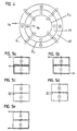
- the supply of the conductor track units E1-E3 with a supply voltage takes place via the supply voltage taps U E, also shown in FIG. 2. In order to enable such field generation, a specific conductor track guidance on the carrier element 10 is required, which will be explained below with reference to FIG. 4.
- both the field of the first and the third conductor track are oriented in the same direction, while the field in the middle of the two conductor tracks is oriented in the opposite direction.
- the corresponding field directions in the two scanning tracks A1, A2 are each indicated in FIG. 4.
- FIGS. 5a-5e represent schematically.
- the principles according to the invention also apply to linear measuring arrangements can be used at any time.
- 5a-5d each reveals possibilities in which the middle conductor track unit in each case an oppositely oriented field to the fields of the two outer ones Track units generated. The result in the two scanning tracks consequently always an oppositely aligned, homogeneous electromagnetic Field in the directions shown.
- the middle conductor track unit is provided in the exemplary embodiment in FIG. 5e between the two scanning tracks in two partial conductor track units divide.
- the two sub-trace units will be flowed through by the current in different directions, although as in the variants explained above, it applies that the immediately adjacent a conductor track units arranged opposite to a scanning track generate an oriented field that forms a homogeneous area in the area of the scanning track Overlay field of defined direction.
- the scanning element arrange several parallel scan tracks on it. So can also more than two scan tracks are provided, each sensor windings with different periodicities, etc. Also for such Arrangements can be made on the basis of the considerations according to the invention the generation of homogeneous excitation fields through the appropriate design and ensure the arrangement of the excitation elements.
- the corresponding routing of the various conductor tracks required for the sensor windings and for the excitation elements on the scanning element can advantageously be realized by a multilayer technique, as is known, for example, from printed circuit board technology.
- a cross section of the scanning element from FIG. 2 is shown in FIG.
- the scanning element 5 of the described embodiment has a seven-layer structure.
- the partial disk, not shown in FIG. 6, faces a first sensor layer SL1, which is separated from a second sensor layer SL2 by a thin, first circuit board layer LP1.
- part of the excitation elements and part of the various sensor windings are arranged.
- the distribution of the excitation elements as well as the sensor windings in the two sensor layers SL1, SL2 has proven to be advantageous in order to avoid undesired line crossings.
- the first printed circuit board layer LP arranged between the two sensor layers it should be noted that this is made as thin as possible, for example in the range 1/10 mm, in order to ensure that in particular the sensor windings arranged in the different sensor layers SL1, SL2 are of the same type conductive graduation areas of the index plate are influenced.
- a thicker, second circuit board layer LP2 which essentially serves to mechanically stabilize the scanning element 5 and is approximately 1-2 mm thick.
- connection layers VL1, VL2 are arranged above them, which are separated by a third circuit board layer LP3.
- the connecting positions VL1, VL2 those conductor tracks are required that are required to supply the excitation elements, to connect the excitation elements, to pick up signals, etc.
- the two-layer design of the connecting layers VL1, VL2 in turn enables the necessary crossover-free routing of such connecting lines.
- the scanning element designed according to the invention can be produced in a multilayer structure of this type in a rational manner using known printed circuit board technologies.
Landscapes
- Physics & Mathematics (AREA)
- General Physics & Mathematics (AREA)
- Transmission And Conversion Of Sensor Element Output (AREA)
- Measurement Of Length, Angles, Or The Like Using Electric Or Magnetic Means (AREA)
- Analogue/Digital Conversion (AREA)
- Body Structure For Vehicles (AREA)
- Vehicle Body Suspensions (AREA)
Applications Claiming Priority (2)
| Application Number | Priority Date | Filing Date | Title |
|---|---|---|---|
| DE19649504 | 1996-11-29 | ||
| DE19649504 | 1996-11-29 |
Publications (3)
| Publication Number | Publication Date |
|---|---|
| EP0845659A2 EP0845659A2 (de) | 1998-06-03 |
| EP0845659A3 EP0845659A3 (de) | 2000-05-17 |
| EP0845659B1 true EP0845659B1 (de) | 2003-06-11 |
Family
ID=7813127
Family Applications (1)
| Application Number | Title | Priority Date | Filing Date |
|---|---|---|---|
| EP97120515A Expired - Lifetime EP0845659B1 (de) | 1996-11-29 | 1997-11-22 | Abtastelement für eine Positionsmesseinrichtung |
Country Status (5)
| Country | Link |
|---|---|
| US (1) | US6111402A (enExample) |
| EP (1) | EP0845659B1 (enExample) |
| JP (1) | JP4001989B2 (enExample) |
| AT (1) | ATE242870T1 (enExample) |
| DE (2) | DE19751853A1 (enExample) |
Cited By (1)
| Publication number | Priority date | Publication date | Assignee | Title |
|---|---|---|---|---|
| WO2023227481A1 (de) | 2022-05-21 | 2023-11-30 | Flux Gmbh | Mehrspuranordnung für linear- und winkelmesssysteme |
Families Citing this family (58)
| Publication number | Priority date | Publication date | Assignee | Title |
|---|---|---|---|---|
| DE19701319C2 (de) * | 1997-01-16 | 2000-06-08 | Heidenhain Gmbh Dr Johannes | Positionsmeßeinrichtung |
| DE19935429C2 (de) * | 1999-07-28 | 2002-01-17 | Daimler Chrysler Ag | Verfahren zur Bestimmung der Winkelposition eines Drehbewegungen ausführenden rotatorischen Teils |
| DE19941464A1 (de) | 1999-09-01 | 2001-03-15 | Hella Kg Hueck & Co | Induktiver Positionssensor |
| DE10032143C2 (de) | 1999-09-30 | 2002-07-18 | Heidenhain Gmbh Dr Johannes | Ferraris-Sensor und Verfahren zum Betrieb eines Ferraris-Sensors |
| JP4889855B2 (ja) * | 2000-02-17 | 2012-03-07 | ドクトル・ヨハネス・ハイデンハイン・ゲゼルシヤフト・ミツト・ベシユレンクテル・ハフツング | 位置測定装置 |
| ATE371167T1 (de) | 2000-02-17 | 2007-09-15 | Heidenhain Gmbh Dr Johannes | Positionsmesseinrichtung und verfahren zu deren betrieb |
| DE10049502A1 (de) | 2000-10-06 | 2002-04-11 | Heidenhain Gmbh Dr Johannes | Verfahren und Vorrichtung zur absoluten Positionsbestimmung |
| EP1248076A1 (de) * | 2001-07-30 | 2002-10-09 | Esec Trading S.A. | Induktiver Sensor für die Positionserfassung eines metallischen Werkstücks |
| DE10158223B4 (de) | 2001-11-16 | 2017-10-05 | Dr. Johannes Heidenhain Gmbh | Drehwinkel-Messgerät |
| DE10200587B4 (de) * | 2002-01-10 | 2015-03-12 | Dr. Johannes Heidenhain Gmbh | Verfahren und Vorrichtung zur inkrementalen Positionsbestimmung |
| DE10320990A1 (de) * | 2003-05-09 | 2004-11-25 | Dr. Johannes Heidenhain Gmbh | Induktiver Drehwinkelsensor und damit ausgestatteter Drehgeber |
| JP4476717B2 (ja) * | 2004-06-30 | 2010-06-09 | オークマ株式会社 | 電磁誘導型位置センサ |
| DE102004037486B4 (de) * | 2004-07-27 | 2006-08-10 | ThyssenKrupp Aufzüge GmbH | Signalband und System zum Bestimmen eines Bewegungszustandes eines bewegten Körpers sowie diese verwendende Vorrichtung zur Geschwindigkeitsbegrenzung des bewegten Körpers, insbesondere eines Aufzugfahrkorbes |
| EP1715298B1 (en) | 2005-04-19 | 2017-07-19 | Mitutoyo Corporation | Absolute rotary encoder and micrometer |
| WO2007068765A1 (de) * | 2005-12-16 | 2007-06-21 | Elmos Semiconductor Ag | Induktiver positionssensor |
| DE102006046531A1 (de) * | 2006-09-29 | 2008-04-03 | Dr. Johannes Heidenhain Gmbh | Drehgeber und Verfahren zu dessen Betrieb |
| DE102006056462A1 (de) | 2006-11-28 | 2008-05-29 | Dr. Johannes Heidenhain Gmbh | Drehgeber |
| DE102006056461A1 (de) | 2006-11-28 | 2008-05-29 | Dr. Johannes Heidenhain Gmbh | Drehgeber |
| JP4960140B2 (ja) * | 2007-04-27 | 2012-06-27 | 株式会社ミツトヨ | 誘導検出型ロータリエンコーダ |
| CN101275988B (zh) * | 2007-12-27 | 2011-08-10 | 奇瑞汽车股份有限公司 | 一种永磁同步电机测试系统及测试方法 |
| DE102008015837A1 (de) * | 2008-03-27 | 2009-10-01 | Dr. Johannes Heidenhain Gmbh | Positionsmessgerät und Verfahren zu dessen Betrieb |
| DE102008017857A1 (de) | 2008-04-09 | 2009-10-15 | Dr. Johannes Heidenhain Gmbh | Induktiver Drehwinkelsensor und Verfahren zum Betrieb eines induktiven Drehwinkelsensors |
| CN101261294B (zh) * | 2008-04-24 | 2010-09-15 | 奇瑞汽车股份有限公司 | 一种永磁电机电感参数测量装置及方法 |
| DE102008046741A1 (de) * | 2008-09-11 | 2010-03-18 | Dr. Johannes Heidenhain Gmbh | Induktiver Positionssensor, damit ausgestattetes Messsystem und Verfahren zum Betrieb eines Positionssensors |
| JP5133199B2 (ja) | 2008-10-28 | 2013-01-30 | 株式会社ミツトヨ | 誘導検出型ロータリーエンコーダ |
| JP5540308B2 (ja) | 2009-10-16 | 2014-07-02 | 株式会社ミツトヨ | ロータリーエンコーダ |
| JP2012247323A (ja) * | 2011-05-30 | 2012-12-13 | Hitachi Automotive Systems Ltd | インダクタンス式回転角度検出装置及びそれを備えたモータ駆動式の絞り弁制御装置 |
| US9007057B2 (en) | 2011-12-28 | 2015-04-14 | Servosence (SMC) Ltd. | High resolution absolute encoder |
| DE102012216854A1 (de) | 2012-09-20 | 2014-03-20 | Dr. Johannes Heidenhain Gmbh | Positionsmessgerät und Verfahren zu dessen Betrieb |
| JP6239824B2 (ja) * | 2013-01-18 | 2017-11-29 | 株式会社ミツトヨ | 誘導検出型ロータリエンコーダ |
| US9164155B2 (en) | 2013-01-29 | 2015-10-20 | Infineon Technologies Ag | Systems and methods for offset reduction in sensor devices and systems |
| US9605983B2 (en) * | 2014-06-09 | 2017-03-28 | Infineon Technologies Ag | Sensor device and sensor arrangement |
| US9823168B2 (en) | 2014-06-27 | 2017-11-21 | Infineon Technologies Ag | Auto tire localization systems and methods utilizing a TPMS angular position index |
| WO2016095882A1 (de) | 2014-12-16 | 2016-06-23 | Balluff Gmbh | Berührungsloser positions-/abstandssensor mit einem künstlichen neuronalen netzwerk und verfahren zu seinem betrieb |
| DE102016202877B3 (de) * | 2016-02-24 | 2017-06-29 | Robert Bosch Gmbh | Drehwinkelsensor |
| DE102016217254B4 (de) * | 2016-09-09 | 2022-02-17 | Robert Bosch Gmbh | Drehwinkelsensor, Statorelement sowie Rotorelement für diesen |
| EP3355032B1 (de) * | 2017-01-30 | 2019-03-27 | Dr. Johannes Heidenhain GmbH | Sensor zur positionsmessung |
| EP3514502B1 (en) * | 2018-01-22 | 2021-07-14 | Melexis Technologies SA | Inductive position sensor |
| US11525701B2 (en) | 2018-01-22 | 2022-12-13 | Melexis Technologies Sa | Inductive position sensor |
| FR3077880B1 (fr) * | 2018-02-15 | 2020-01-17 | Continental Automotive France | Capteur de couple integrant un capteur de position angulaire d'un element en rotation |
| DE102018217934A1 (de) | 2018-10-19 | 2020-04-23 | Dr. Johannes Heidenhain Gesellschaft Mit Beschränkter Haftung | Positionsmesseinrichtung und Verfahren zum Betreiben einer Positionsmesseinrichtung |
| EP3683551B1 (de) | 2019-01-17 | 2021-03-10 | Dr. Johannes Heidenhain GmbH | Abtasteinheit für eine winkelmesseinrichtung |
| ES2870327T3 (es) | 2019-01-17 | 2021-10-26 | Heidenhain Gmbh Dr Johannes | Unidad de exploración para un dispositivo de medición de ángulos |
| DE102019214219A1 (de) * | 2019-09-18 | 2021-03-18 | Dr. Johannes Heidenhain Gesellschaft Mit Beschränkter Haftung | Messeinrichtung |
| EP3936829B1 (en) * | 2020-07-10 | 2023-08-30 | Renesas Electronics America Inc. | Inductive position sensor comprising at least one transmit coil, an absolute position receive coil pair, a high-resolution position receive coil pair and a conductive moving target |
| EP3961158B1 (de) * | 2020-08-25 | 2022-11-23 | Dr. Johannes Heidenhain GmbH | Abtastelement und induktive positionsmesseinrichtung mit diesem abtastelement |
| US11598654B2 (en) | 2020-12-14 | 2023-03-07 | Microchip Technology Inc. | High resolution angular inductive sensor and associated method of use |
| WO2022132229A1 (en) * | 2020-12-14 | 2022-06-23 | Microchip Technology Inc. | High resolution angular inductive sensor and associated method of use |
| WO2022203740A1 (en) | 2021-03-25 | 2022-09-29 | Microchip Technology Incorporated | Sense coil for inductive rotational-position sensing, and related devices, systems, and methods |
| EP4086586B1 (en) | 2021-05-03 | 2026-02-11 | Vishay MCB Industrie S.A.S. | Position encoder |
| CN117501071A (zh) | 2021-06-11 | 2024-02-02 | 微芯片技术股份有限公司 | 用于感应线性位置感测的感测线圈以及相关设备、系统和方法 |
| US12031817B2 (en) | 2021-08-05 | 2024-07-09 | Microchip Technology Incorporated | Inductive angular-position sensors, and related devices, systems, and methods |
| US12339139B2 (en) | 2021-09-28 | 2025-06-24 | Microchip Technology Incorporated | Angular-position sensor |
| US12411001B2 (en) | 2022-04-01 | 2025-09-09 | Microchip Technology Incorporated | Target for inductive angular-position sensing |
| WO2023191900A1 (en) | 2022-04-01 | 2023-10-05 | Microchip Technology Incorporated | Target for an inductive angular-position sensor |
| CN114838655B (zh) * | 2022-04-12 | 2023-04-07 | 北京科技大学 | 一种多周期双极型电磁感应式角度传感器 |
| EP4273507B1 (de) | 2022-05-05 | 2024-07-10 | Dr. Johannes Heidenhain GmbH | Abtastelement und induktive positionsmesseinrichtung mit diesem abtastelement |
| DE102024203299A1 (de) * | 2024-04-11 | 2025-10-16 | Robert Bosch Gesellschaft mit beschränkter Haftung | Induktive Sensoranordnung zur Erfassung einer Bewegung eines beweglichen Körpers |
Family Cites Families (22)
| Publication number | Priority date | Publication date | Assignee | Title |
|---|---|---|---|---|
| US3197763A (en) * | 1962-08-28 | 1965-07-27 | Electro Mechanical Res Inc | Shaft encoders |
| US3281826A (en) * | 1963-03-20 | 1966-10-25 | United Aircraft Corp | Non-contacting encoder |
| GB1414517A (en) * | 1971-11-26 | 1975-11-19 | Bosch Gmbh Robert | Rotary inductive transducers |
| US3810136A (en) * | 1973-02-15 | 1974-05-07 | Singer Co | Digital position sensor |
| NL7900245A (nl) * | 1979-01-12 | 1980-07-15 | Philips Nv | Tweelaags vlakke electrische spoel met aftakking. |
| DE3214794C2 (de) * | 1982-04-21 | 1984-06-07 | Dr. Johannes Heidenhain Gmbh, 8225 Traunreut | Magnetische Längen- oder Winkelmeßeinrichtung |
| US4697144A (en) * | 1984-04-19 | 1987-09-29 | Verify Electronics Limited | Position sensing apparatus |
| IE55855B1 (en) * | 1984-10-19 | 1991-01-30 | Kollmorgen Ireland Ltd | Position and speed sensors |
| JPH0665967B2 (ja) * | 1985-08-27 | 1994-08-24 | 株式会社エスジー | アブソリュート回転位置検出装置 |
| US4985691A (en) * | 1986-02-26 | 1991-01-15 | University Of Pittsburgh | Contactless motion sensor |
| IE871118L (en) * | 1987-05-01 | 1988-11-01 | Univ Manchester | Improvements in or relating to linear motion screened¹inductance sensors. |
| US4853631A (en) * | 1987-11-04 | 1989-08-01 | The Superior Electric Company | Magnetoresistive sensor having inter-leaved magnetoresistive elements for detecting encoded magnetic information |
| DE3813949A1 (de) * | 1988-04-26 | 1989-11-09 | Heidenhain Gmbh Dr Johannes | Vorrichtung zur induktiven signaluebertragung bei tastkoepfen |
| DE4021637A1 (de) * | 1990-07-06 | 1992-01-09 | Mehnert Walter Dipl Ing Dr Ing | Induktiver stellungsgeber |
| DE4127209C2 (de) * | 1991-08-16 | 1996-05-23 | Mehnert Walter Dr | Geber zur induktiven Erzeugung eines Meßsignals |
| DE59304986D1 (de) * | 1993-04-10 | 1997-02-13 | Heidenhain Gmbh Dr Johannes | Magnetisches Messsystem |
| DE4316221C2 (de) * | 1993-05-14 | 1995-11-23 | Heidenhain Gmbh Dr Johannes | Positionsmeßeinrichtung |
| DE4319322C2 (de) * | 1993-06-11 | 1998-04-23 | Heidenhain Gmbh Dr Johannes | Positionsmeßeinrichtung |
| DE19504307A1 (de) * | 1995-02-09 | 1996-08-14 | Siemens Ag | Einrichtung zur Erfassung von Position und/oder Geschwindigkeit eines beweglichen Geräteteils |
| EP0743508A2 (en) * | 1995-05-16 | 1996-11-20 | Mitutoyo Corporation | Induced current position transducer |
| GB9523991D0 (en) * | 1995-11-23 | 1996-01-24 | Scient Generics Ltd | Position encoder |
| US5841274A (en) * | 1997-01-29 | 1998-11-24 | Mitutoyo Corporation | Induced current absolute position transducer using a code-track-type scale and read head |
-
1997
- 1997-11-19 JP JP31859997A patent/JP4001989B2/ja not_active Expired - Lifetime
- 1997-11-22 AT AT97120515T patent/ATE242870T1/de not_active IP Right Cessation
- 1997-11-22 DE DE19751853A patent/DE19751853A1/de not_active Withdrawn
- 1997-11-22 DE DE59710260T patent/DE59710260D1/de not_active Expired - Lifetime
- 1997-11-22 EP EP97120515A patent/EP0845659B1/de not_active Expired - Lifetime
- 1997-11-25 US US08/977,706 patent/US6111402A/en not_active Expired - Lifetime
Cited By (1)
| Publication number | Priority date | Publication date | Assignee | Title |
|---|---|---|---|---|
| WO2023227481A1 (de) | 2022-05-21 | 2023-11-30 | Flux Gmbh | Mehrspuranordnung für linear- und winkelmesssysteme |
Also Published As
| Publication number | Publication date |
|---|---|
| US6111402A (en) | 2000-08-29 |
| DE59710260D1 (de) | 2003-07-17 |
| JPH10213407A (ja) | 1998-08-11 |
| ATE242870T1 (de) | 2003-06-15 |
| JP4001989B2 (ja) | 2007-10-31 |
| EP0845659A3 (de) | 2000-05-17 |
| DE19751853A1 (de) | 1998-06-04 |
| EP0845659A2 (de) | 1998-06-03 |
Similar Documents
| Publication | Publication Date | Title |
|---|---|---|
| EP0845659B1 (de) | Abtastelement für eine Positionsmesseinrichtung | |
| EP1475604A2 (de) | Induktiver Drehwinkelsensor | |
| EP4012351B1 (de) | Abtastelement und induktive positionsmesseinrichtung mit diesem abtastelement | |
| EP3179214B1 (de) | Induktive positionsmesseinrichtung | |
| EP2329225B1 (de) | Induktiver positionssensor, damit ausgestattetes messsystem und verfahren zum betrieb eines positionssensors | |
| EP3961158B1 (de) | Abtastelement und induktive positionsmesseinrichtung mit diesem abtastelement | |
| DE10158223A1 (de) | Drehwinkel-Messgerät | |
| EP4174443A1 (de) | Induktive winkelmesseinrichtung | |
| DE69930341T2 (de) | Kodierer zur Lieferung von inkrementalen und absoluten Positionswerten | |
| EP4012350B1 (de) | Abtastelement und induktive positionsmesseinrichtung mit diesem abtastelement | |
| EP1111345A2 (de) | Positionsmesseinrichtung | |
| DE4129576C2 (de) | Magnetisches Meßsystem zur Drehwinkelmessung | |
| EP3901582B1 (de) | Induktive winkelmesseinrichtung | |
| EP4012349B1 (de) | Abtastelement und induktive positionsmesseinrichtung mit diesem abtastelement | |
| EP3904836A1 (de) | Induktive positionsmesseinrichtung | |
| EP4273507B1 (de) | Abtastelement und induktive positionsmesseinrichtung mit diesem abtastelement | |
| EP4421453B1 (de) | Abtastelement für eine induktive winkelmesseinrichrung | |
| DE29724833U1 (de) | Abtastelement für eine Positionsmeßeinrichtung | |
| EP3929539A1 (de) | Abtasteinheit und damit ausgestatteter drehgeber | |
| EP4530581B1 (de) | Abtastelement für eine induktive positionsmesseinrichtung | |
| EP4421454B1 (de) | Skalenelement für eine induktive positionsmesseinrichtung | |
| EP4567381B1 (de) | Induktive positionsmesseinrichtung | |
| DE102023102164B4 (de) | Sekundärspulenanordnung für einen induktiven Encoder | |
| EP4484897B1 (de) | Induktive winkelmesseinrichtung | |
| EP4647726A1 (de) | Positionsmesseinrichtung |
Legal Events
| Date | Code | Title | Description |
|---|---|---|---|
| PUAI | Public reference made under article 153(3) epc to a published international application that has entered the european phase |
Free format text: ORIGINAL CODE: 0009012 |
|
| AK | Designated contracting states |
Kind code of ref document: A2 Designated state(s): AT CH DE FR GB IT LI |
|
| AX | Request for extension of the european patent |
Free format text: AL;LT;LV;MK;RO;SI |
|
| PUAL | Search report despatched |
Free format text: ORIGINAL CODE: 0009013 |
|
| AK | Designated contracting states |
Kind code of ref document: A3 Designated state(s): AT BE CH DE DK ES FI FR GB GR IE IT LI LU MC NL PT SE |
|
| 17P | Request for examination filed |
Effective date: 20001117 |
|
| AKX | Designation fees paid |
Free format text: AT CH DE FR GB IT LI |
|
| 17Q | First examination report despatched |
Effective date: 20020621 |
|
| GRAH | Despatch of communication of intention to grant a patent |
Free format text: ORIGINAL CODE: EPIDOS IGRA |
|
| GRAH | Despatch of communication of intention to grant a patent |
Free format text: ORIGINAL CODE: EPIDOS IGRA |
|
| GRAA | (expected) grant |
Free format text: ORIGINAL CODE: 0009210 |
|
| AK | Designated contracting states |
Designated state(s): AT CH DE FR GB IT LI |
|
| REG | Reference to a national code |
Ref country code: GB Ref legal event code: FG4D Free format text: NOT ENGLISH |
|
| REG | Reference to a national code |
Ref country code: CH Ref legal event code: EP |
|
| REG | Reference to a national code |
Ref country code: CH Ref legal event code: NV Representative=s name: TROESCH SCHEIDEGGER WERNER AG |
|
| REF | Corresponds to: |
Ref document number: 59710260 Country of ref document: DE Date of ref document: 20030717 Kind code of ref document: P |
|
| GBT | Gb: translation of ep patent filed (gb section 77(6)(a)/1977) | ||
| ET | Fr: translation filed | ||
| PLBE | No opposition filed within time limit |
Free format text: ORIGINAL CODE: 0009261 |
|
| STAA | Information on the status of an ep patent application or granted ep patent |
Free format text: STATUS: NO OPPOSITION FILED WITHIN TIME LIMIT |
|
| 26N | No opposition filed |
Effective date: 20040312 |
|
| PGFP | Annual fee paid to national office [announced via postgrant information from national office to epo] |
Ref country code: AT Payment date: 20081114 Year of fee payment: 12 |
|
| PG25 | Lapsed in a contracting state [announced via postgrant information from national office to epo] |
Ref country code: AT Free format text: LAPSE BECAUSE OF NON-PAYMENT OF DUE FEES Effective date: 20091122 |
|
| PGFP | Annual fee paid to national office [announced via postgrant information from national office to epo] |
Ref country code: FR Payment date: 20121130 Year of fee payment: 16 Ref country code: CH Payment date: 20121122 Year of fee payment: 16 |
|
| PGFP | Annual fee paid to national office [announced via postgrant information from national office to epo] |
Ref country code: IT Payment date: 20121123 Year of fee payment: 16 Ref country code: GB Payment date: 20121120 Year of fee payment: 16 |
|
| REG | Reference to a national code |
Ref country code: CH Ref legal event code: PL |
|
| GBPC | Gb: european patent ceased through non-payment of renewal fee |
Effective date: 20131122 |
|
| PG25 | Lapsed in a contracting state [announced via postgrant information from national office to epo] |
Ref country code: LI Free format text: LAPSE BECAUSE OF NON-PAYMENT OF DUE FEES Effective date: 20131130 Ref country code: CH Free format text: LAPSE BECAUSE OF NON-PAYMENT OF DUE FEES Effective date: 20131130 |
|
| REG | Reference to a national code |
Ref country code: FR Ref legal event code: ST Effective date: 20140731 |
|
| PG25 | Lapsed in a contracting state [announced via postgrant information from national office to epo] |
Ref country code: IT Free format text: LAPSE BECAUSE OF NON-PAYMENT OF DUE FEES Effective date: 20131122 |
|
| PG25 | Lapsed in a contracting state [announced via postgrant information from national office to epo] |
Ref country code: FR Free format text: LAPSE BECAUSE OF NON-PAYMENT OF DUE FEES Effective date: 20131202 Ref country code: GB Free format text: LAPSE BECAUSE OF NON-PAYMENT OF DUE FEES Effective date: 20131122 |
|
| PGFP | Annual fee paid to national office [announced via postgrant information from national office to epo] |
Ref country code: DE Payment date: 20151119 Year of fee payment: 19 |
|
| REG | Reference to a national code |
Ref country code: DE Ref legal event code: R119 Ref document number: 59710260 Country of ref document: DE |
|
| PG25 | Lapsed in a contracting state [announced via postgrant information from national office to epo] |
Ref country code: DE Free format text: LAPSE BECAUSE OF NON-PAYMENT OF DUE FEES Effective date: 20170601 |