EP0844508A2 - Vorrichtung und Verfahren zur optischen Modulation - Google Patents
Vorrichtung und Verfahren zur optischen Modulation Download PDFInfo
- Publication number
- EP0844508A2 EP0844508A2 EP97309510A EP97309510A EP0844508A2 EP 0844508 A2 EP0844508 A2 EP 0844508A2 EP 97309510 A EP97309510 A EP 97309510A EP 97309510 A EP97309510 A EP 97309510A EP 0844508 A2 EP0844508 A2 EP 0844508A2
- Authority
- EP
- European Patent Office
- Prior art keywords
- optical
- modulation
- modulator
- circuit
- amplifying circuit
- Prior art date
- Legal status (The legal status is an assumption and is not a legal conclusion. Google has not performed a legal analysis and makes no representation as to the accuracy of the status listed.)
- Withdrawn
Links
Images


Classifications
-
- G—PHYSICS
- G02—OPTICS
- G02F—OPTICAL DEVICES OR ARRANGEMENTS FOR THE CONTROL OF LIGHT BY MODIFICATION OF THE OPTICAL PROPERTIES OF THE MEDIA OF THE ELEMENTS INVOLVED THEREIN; NON-LINEAR OPTICS; FREQUENCY-CHANGING OF LIGHT; OPTICAL LOGIC ELEMENTS; OPTICAL ANALOGUE/DIGITAL CONVERTERS
- G02F1/00—Devices or arrangements for the control of the intensity, colour, phase, polarisation or direction of light arriving from an independent light source, e.g. switching, gating or modulating; Non-linear optics
- G02F1/01—Devices or arrangements for the control of the intensity, colour, phase, polarisation or direction of light arriving from an independent light source, e.g. switching, gating or modulating; Non-linear optics for the control of the intensity, phase, polarisation or colour
- G02F1/0121—Operation of devices; Circuit arrangements, not otherwise provided for in this subclass
- G02F1/0123—Circuits for the control or stabilisation of the bias voltage, e.g. automatic bias control [ABC] feedback loops
Definitions
- the present invention relates to an optical modulation apparatus and an optical modulation method, and more particularly to an optical modulation apparatus and an optical modulation method for controlling modulation drive signals.
- waveguide type optical modulators are used.
- waveguide type optical modulators ones using LiNbO3 for their substrates are well known, and they can be classified into three types: light intensity modulators, optical phase modulators and optical polarization modulators.
- optical modulation circuit in which, out of these waveguide type optical modulators, an optical polarization modulator is used.
- the optical polarization modulator there are installed an optical input port to which optical signals are inputted and an optical output port from which polarization-modulated signals are outputted.
- the optical polarization modulator is also provided with an amplifying circuit for outputting modulation drive signals corresponding to polarization-modulation signals.
- modulation drive signals are inputted to an electric signal input port of the optical polarization modulator and, traveling over a strip electrode line inside, outputted from an electric signal output.
- the modulation drive signals are terminated by a terminating circuit matched to the characteristic impedance of the strip electrode line.
- optical modulation apparatuses involve the problem that they are not disposed to cause the gain of said amplifying circuit to be controlled in any particular way. Therefore, if modulation input signals to the amplifying circuit vary in amplitude or its ambient temperature changes, the amplitude of modulation drive signals supplied from the amplifying circuit will vary. More specifically, a temperature rise would bring down the gain of the amplifying circuit.
- an optical polarization modulator is used as a waveguide type optical modulator
- any variation in the amplitude of modulation drive signals would invite a change in the quantity of polarization modulation and a deterioration in the degree of polarization (referred to "DOP", hereinafter).
- DOP degree of polarization
- a light intensity type waveguide type optical modulator would deteriorate in quenching ratio.
- An optical modulation apparatus is provided with an optical modulator for modulating optical signals, an amplifying circuit for amplifying modulation input signals and supplying modulation drive signals to said optical modulator, a detecting circuit for detecting the modulation drive signals supplied from said optical modulator, and a control circuit for controlling said amplifying circuit according to the signals supplied by said detecting circuit.
- An optical modulation method comprises detecting modulation drive signals supplied from an optical modulator, and controlling an amplifying circuit for supplying the optical modulator with modulation control signals on the basis of the detected modulation drive signals.
- Optical modulation apparatus and optical modulation methods embodying the invention can be arranged to manifest stable optical modulation characteristics.
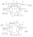
- an optical modulation apparatus In an optical polarization modulator 11, an optical signal is inputted from an optical signal input port 5, and a modulated optical signal is outputted from an optical signal output port 6.
- An amplifying circuit 12 amplifies a modulation input signal, and delivers it from an electric signal input port 7 to the optical polarization modulator 11. This input signal is outputted from an electric signal output port 8, and terminated by a terminating circuit 13 matched to the characteristic impedance of a strip electrode line.
- the modulation input signal entered from the amplifying circuit 12 is subject to no particular control. Therefore, the dependence of polarization by the known optical polarization modulator 11 of Fig. 1 upon ambient temperature is such that, as shown in Fig. 2, DOP may vary by up to, for instance, 30%.
- the optical modulation apparatus has a waveguide type optical modulator 2 for modulating optical signals and a variable gain amplifying circuit 1 for supplying modulation drive signals to the waveguide type optical modulator 2.
- the waveguide type optical modulator 2 composed of a traveling-wave electrode structure in which optical signals and modulation drive signals travel in the same direction, has an optical waveguide 9 and a strip electrode line 10.
- An optical signal travels from an optical signal input port 5 over the optical waveguide 9 and is supplied to an optical signal output port 6.
- a modulating drive signal is entered from the variable gain amplifying circuit 1 into an electric signal input port 7, and travels over the strip electrode line 10 to be supplied to an electric signal output port 8.
- the variable gain amplifying circuit 1 amplifies the modulation input signal, which is a clock signal, and supplies it to the electric signal input port as modulation drive signal.
- a peak detecting circuit 3 To the electric signal output port 8 is connected a peak detecting circuit 3.
- This peak detecting circuit 3 detects, and supplies to a gain control circuit 4, a voltage signal corresponding to the amplitude of the modulation drive signal having traveled over the strip electrode line 10.
- the gain control circuit 4 controls the gain of the variable gain amplifying circuit 1 so that said voltage signal be identical with a preset reference voltage Vs.
- This reference voltage Vs is a voltage to generate the currently set level of modulation.
- the waveguide optical modulator 2 there is available a light intensity modulator, an optical phase modulator or an optical polarization modulator, differentiated from each other by the structure of the waveguide or the incidence structure for optical signals, and the present invention is adaptable to any of them.
- a modulation drive signal brought to incidence from the variable gain amplifying circuit 1 upon the waveguide type optical modulator 2 is detected by a peak detecting circuit 3 connected to the electric signal output port 8.
- This peak detecting circuit 3 detects the peak voltage of demodulation drive signals.
- the gain control circuit 4 compares the peak voltage with a prescribed reference voltage Vs, and applies feedback control on the variable gain amplifying circuit 1 so as to equalize the peak voltage to the reference voltage Vs. For this reason, the variable gain amplifying circuit 1 can always feed the waveguide type optical modulator 2 with modulation drive signals of a constant amplitude. As a result, even if the variable gain amplifying circuit 1 is affected by any change in ambient conditions including temperature, or if modulation drive signals fluctuate in amplitude, this waveguide type optical modulator 2 can manifest steady optical modulation characteristics.
- an optical polarization modulator is used as waveguide type optical modulator 2 of an optical modulation apparatus according to the present invention as waveguide type optical modulator 2 of an optical modulation apparatus according to the present invention is illustrated in Fig. 4.
- the clock frequency of modulation input signals entered into the variable gain amplifying circuit 1 is 5 GHz.
- optical polarization modulator 11 to modulate the state of polarization of optical signals, including digital data there is used a LiNbO3 waveguide type optical modulator. Its 2V ⁇ voltage amplitude is 8.2 Vpp at 5 GHz, while the transmission loss of the strip electrode line is -2 dB at 5 GHz.
- the variable gain amplifying circuit 1 using a GaAs field effect transistor, can vary the gain from -30 dB to +20 dB with its gate voltage, and its saturation output power is +23 dBm.
- Fig. 5 shows the basic characteristics of DOP of the optical polarization modulator 11 used here vis-a-vis the amplitude of the modulation drive signal.
- the vertical axis of the graph represents DOP of the optical modulator, while the horizontal axis represents the peak-to-peak amplitude of the modulation drive signal supplied by the variable gain amplifying circuit 1.
- this modulation drive signal varies in a sine curve.
- DOP varies as the amplitude of the modulation drive signal supplied by the variable gain amplifying circuit 1 varies under the effect of ambient temperature variation.
- Fig. 5 shows the minimum DOP of 5% at 8.2 Vpp. Fig.
- Fig. 7 shows the relationship between ambient temperature and DOP when the ambient temperature is varied from 5°C to 50°C under feedback control, indicating that the variation of DOP is always kept from exceeding 8%.
- an optical modulation apparatus can achieve steady optical modulation characteristics against fluctuations in the amplitude of modulated input signals or in ambient temperature.
- the peak detecting circuit 3 detects the peak values of signals supplied from the electric signal output port 8, but the mean value, instead of the peak value, may as well be detected.
Landscapes
- Physics & Mathematics (AREA)
- Nonlinear Science (AREA)
- General Physics & Mathematics (AREA)
- Optics & Photonics (AREA)
- Optical Communication System (AREA)
Applications Claiming Priority (2)
| Application Number | Priority Date | Filing Date | Title |
|---|---|---|---|
| JP314480/96 | 1996-11-26 | ||
| JP8314480A JP2820138B2 (ja) | 1996-11-26 | 1996-11-26 | 光変調装置 |
Publications (2)
| Publication Number | Publication Date |
|---|---|
| EP0844508A2 true EP0844508A2 (de) | 1998-05-27 |
| EP0844508A3 EP0844508A3 (de) | 1998-12-23 |
Family
ID=18053825
Family Applications (1)
| Application Number | Title | Priority Date | Filing Date |
|---|---|---|---|
| EP97309510A Withdrawn EP0844508A3 (de) | 1996-11-26 | 1997-11-26 | Vorrichtung und Verfahren zur optischen Modulation |
Country Status (3)
| Country | Link |
|---|---|
| US (1) | US6335991B1 (de) |
| EP (1) | EP0844508A3 (de) |
| JP (1) | JP2820138B2 (de) |
Families Citing this family (1)
| Publication number | Priority date | Publication date | Assignee | Title |
|---|---|---|---|---|
| AUPS169302A0 (en) * | 2002-04-11 | 2002-05-16 | Bishop Steering Technology Limited | Method for manufacturing a directionally dependent reflective surface |
Citations (2)
| Publication number | Priority date | Publication date | Assignee | Title |
|---|---|---|---|---|
| JPH0373916A (ja) * | 1989-08-15 | 1991-03-28 | Fujitsu Ltd | 光変調器の駆動方式 |
| JPH05264934A (ja) * | 1992-03-23 | 1993-10-15 | Nec Corp | 光変調器駆動回路 |
Family Cites Families (11)
| Publication number | Priority date | Publication date | Assignee | Title |
|---|---|---|---|---|
| US3950237A (en) * | 1972-12-14 | 1976-04-13 | Mitsubishi Kasei Kogyo Kabushiki Kaisha | Coulometric titrating devices |
| JPS5574223A (en) * | 1978-11-30 | 1980-06-04 | Tdk Corp | Trimming unit |
| GB2192272B (en) * | 1986-07-02 | 1990-06-06 | Cossor Electronics Ltd | Spectrum analyser |
| US4970391A (en) * | 1987-01-27 | 1990-11-13 | Medrad, Inc. | Radiation detector with an ionizable gas atop an integrated circuit |
| JPH0816743B2 (ja) * | 1988-08-05 | 1996-02-21 | 国際電信電話株式会社 | 光変調素子 |
| NL8802544A (nl) * | 1988-10-17 | 1990-05-16 | Philips Nv | Ontvanger voor toepassing in een afstandsbedieningssysteem. |
| CA2083219C (en) * | 1991-11-19 | 1999-01-05 | Hiroshi Nishimoto | Optical transmitter having optical modulator |
| US5258869A (en) * | 1992-12-31 | 1993-11-02 | Xerox Corporation | Xerographic laser light modulation with built-in light leveling using optical circulators |
| JP2518138B2 (ja) * | 1993-06-25 | 1996-07-24 | 日本電気株式会社 | 光変調装置 |
| JP3263553B2 (ja) * | 1994-02-23 | 2002-03-04 | キヤノン株式会社 | 光送信機 |
| JP2677234B2 (ja) * | 1995-03-17 | 1997-11-17 | 日本電気株式会社 | 光変調装置 |
-
1996
- 1996-11-26 JP JP8314480A patent/JP2820138B2/ja not_active Expired - Fee Related
-
1997
- 1997-11-24 US US08/977,266 patent/US6335991B1/en not_active Expired - Fee Related
- 1997-11-26 EP EP97309510A patent/EP0844508A3/de not_active Withdrawn
Patent Citations (2)
| Publication number | Priority date | Publication date | Assignee | Title |
|---|---|---|---|---|
| JPH0373916A (ja) * | 1989-08-15 | 1991-03-28 | Fujitsu Ltd | 光変調器の駆動方式 |
| JPH05264934A (ja) * | 1992-03-23 | 1993-10-15 | Nec Corp | 光変調器駆動回路 |
Non-Patent Citations (2)
| Title |
|---|
| PATENT ABSTRACTS OF JAPAN vol. 015, no. 237 (P-1216), 19 June 1991 -& JP 03 073916 A (FUJITSU LTD), 28 March 1991 * |
| PATENT ABSTRACTS OF JAPAN vol. 018, no. 036 (P-1678), 19 January 1994 -& JP 05 264934 A (NEC CORP), 15 October 1993 * |
Also Published As
| Publication number | Publication date |
|---|---|
| EP0844508A3 (de) | 1998-12-23 |
| JP2820138B2 (ja) | 1998-11-05 |
| JPH10153757A (ja) | 1998-06-09 |
| US6335991B1 (en) | 2002-01-01 |
Similar Documents
| Publication | Publication Date | Title |
|---|---|---|
| JP3583846B2 (ja) | 光変調器の駆動方法及び装置並びに光通信システム | |
| US6362913B2 (en) | Optical modulation apparatus and method of controlling optical modulator | |
| US6490071B2 (en) | Method and apparatus for optimizing SBS performance in an optical communication system using at least two phase modulation tones | |
| US7215894B2 (en) | Optical transmitter device | |
| US5706116A (en) | Drive circuit optical modulator and optical transmitter | |
| US6590686B1 (en) | Optical transmitter | |
| JP2642499B2 (ja) | 光送信器、光変調器の制御回路および光変調方法 | |
| US5771255A (en) | Laser light generator | |
| US5317443A (en) | Optical transmitter | |
| US20150071583A1 (en) | Optical modulator and optical modulation control method | |
| EP0565306A1 (de) | Lichtwellensender mit Modulator | |
| US7630651B2 (en) | Method and apparatus for controlling bias point of optical transmitter | |
| US7023534B2 (en) | Optical modulating apparatus having bias controller and bias control method | |
| US20050105917A1 (en) | Optical modulating apparatus | |
| US5805328A (en) | Driving circuit for an optical signal modulator | |
| US11381316B2 (en) | Optical transmitter and optical transmission method | |
| EP0844508A2 (de) | Vorrichtung und Verfahren zur optischen Modulation | |
| US6473219B1 (en) | Method and apparatus for asymetrical optical modulation | |
| JP2001350128A (ja) | 光送信器 | |
| US6334005B1 (en) | Modulator of the Mach-Zehnder type having a very high extinction ratio | |
| US20230388016A1 (en) | Optimization of rf driver and/or optical device | |
| US7257332B2 (en) | Optical transmitter and its control method | |
| US5745282A (en) | Light modulation device | |
| EP0607849B1 (de) | Amplitudenstabilisierkreis für eine optische Glasfaserverbindung | |
| JP3406152B2 (ja) | 光変調器駆動回路 |
Legal Events
| Date | Code | Title | Description |
|---|---|---|---|
| PUAI | Public reference made under article 153(3) epc to a published international application that has entered the european phase |
Free format text: ORIGINAL CODE: 0009012 |
|
| AK | Designated contracting states |
Kind code of ref document: A2 Designated state(s): FR GB IT |
|
| AX | Request for extension of the european patent |
Free format text: AL;LT;LV;MK;RO;SI |
|
| PUAL | Search report despatched |
Free format text: ORIGINAL CODE: 0009013 |
|
| AK | Designated contracting states |
Kind code of ref document: A3 Designated state(s): AT BE CH DE DK ES FI FR GB GR IE IT LI LU MC NL PT SE |
|
| AX | Request for extension of the european patent |
Free format text: AL;LT;LV;MK;RO;SI |
|
| 17P | Request for examination filed |
Effective date: 19990311 |
|
| AKX | Designation fees paid |
Free format text: FR GB IT |
|
| REG | Reference to a national code |
Ref country code: DE Ref legal event code: 8566 |
|
| 17Q | First examination report despatched |
Effective date: 20040407 |
|
| STAA | Information on the status of an ep patent application or granted ep patent |
Free format text: STATUS: THE APPLICATION IS DEEMED TO BE WITHDRAWN |
|
| 18D | Application deemed to be withdrawn |
Effective date: 20040818 |