EP0843889B1 - Vorrichtung und verfahren zur laser-oberflächenbehandlung - Google Patents
Vorrichtung und verfahren zur laser-oberflächenbehandlung Download PDFInfo
- Publication number
- EP0843889B1 EP0843889B1 EP96924926A EP96924926A EP0843889B1 EP 0843889 B1 EP0843889 B1 EP 0843889B1 EP 96924926 A EP96924926 A EP 96924926A EP 96924926 A EP96924926 A EP 96924926A EP 0843889 B1 EP0843889 B1 EP 0843889B1
- Authority
- EP
- European Patent Office
- Prior art keywords
- zone
- laser
- energy
- ellipsometry
- laser beam
- Prior art date
- Legal status (The legal status is an assumption and is not a legal conclusion. Google has not performed a legal analysis and makes no representation as to the accuracy of the status listed.)
- Expired - Lifetime
Links
Images



Classifications
-
- B—PERFORMING OPERATIONS; TRANSPORTING
- B24—GRINDING; POLISHING
- B24B—MACHINES, DEVICES, OR PROCESSES FOR GRINDING OR POLISHING; DRESSING OR CONDITIONING OF ABRADING SURFACES; FEEDING OF GRINDING, POLISHING, OR LAPPING AGENTS
- B24B37/00—Lapping machines or devices; Accessories
- B24B37/005—Control means for lapping machines or devices
- B24B37/013—Devices or means for detecting lapping completion
-
- H—ELECTRICITY
- H10—SEMICONDUCTOR DEVICES; ELECTRIC SOLID-STATE DEVICES NOT OTHERWISE PROVIDED FOR
- H10P—GENERIC PROCESSES OR APPARATUS FOR THE MANUFACTURE OR TREATMENT OF DEVICES COVERED BY CLASS H10
- H10P74/00—Testing or measuring during manufacture or treatment of wafers, substrates or devices
-
- H—ELECTRICITY
- H10—SEMICONDUCTOR DEVICES; ELECTRIC SOLID-STATE DEVICES NOT OTHERWISE PROVIDED FOR
- H10P—GENERIC PROCESSES OR APPARATUS FOR THE MANUFACTURE OR TREATMENT OF DEVICES COVERED BY CLASS H10
- H10P74/00—Testing or measuring during manufacture or treatment of wafers, substrates or devices
- H10P74/23—Testing or measuring during manufacture or treatment of wafers, substrates or devices characterised by multiple measurements, corrections, marking or sorting processes
- H10P74/238—Testing or measuring during manufacture or treatment of wafers, substrates or devices characterised by multiple measurements, corrections, marking or sorting processes comprising acting in response to an ongoing measurement without interruption of processing, e.g. endpoint detection or in-situ thickness measurement
Definitions
- the invention relates to surface treatment by laser, and its control.
- the application of a laser beam on the purpose of a surface is to modify said surface, its structure and condition.
- the mechanism involved is a partial fusion of the surface, in the case of silicon crystallization amorphous.
- the Applicant has posed the problem of providing device and method capable of controlling, in real time, on-site, quickly and non-destructively treatment surface area by laser in which there is at least two generally similar superficial areas to be treated, of given depth, on each of which must be applied, in one or more times, a laser treatment beam, characteristics chosen to change the physical state of each surface area.
- the present invention provides a solution to this problem / and provides a method according to claim 1 and a device according to claim 12.
- the method is characterized by taking at least one measurement of ellipsometry before at least one of the applications of the processing beam on the second surface area, in at least one area of the first surface domain, so to obtain a characterization of said first surface domain, which allows time control real, on site, nondestructively and quickly, the change of physical state of each surface area to using said characterization.
- the measurement of ellipsometry is spectroscopic.
- the measurement ellipsometry is performed at one or a few lengths wave.
- the Applicant has observed that it is possible to ensure that the domain of ellipsometry analysis substantially covers (in depth, but occasionally) the surface area three-dimensional (often referred to hereinafter as "surface", to simplify) which is affected by the impact of the laser beam. This opens up many possibilities for processing control different layers of said surface. Furthermore, it has been observed that this analysis and laser treatment can be implemented according to working conditions generally similar by means of metrology and / or relatively simple and inexpensive optics, which facilitates obtaining a reduced size, and further contributes to reduce the costs of implementing the process and device of the invention.
- the Applicant has observed that the time interval between two applications of a strong laser beam power allows at least one ellipsometry measurement between said laser applications.
- the Applicant has also observed that the characterization physico-chemical by ellipsometry allows not only a control, done before and / or after laser treatment, but also the optimization of at least some of the parameters of said laser treatment.
- this optimization of the laser treatment takes place according to a predetermined law depending at least on part of said physico-chemical characterization before each step of the laser treatment.
- one of the parameters of the optimization of the laser treatment is the energy applied by the beam laser per unit area and / or per unit time.
- optimizing laser treatment involves to adjust the energy per unit area and / or per unit of time brought by the laser source to obtain a beam laser suitable for the surface area to be treated, in accordance to the characterization of this domain obtained by ellipsometry Spectroscopic. Specifically, this adjustment consists in varying the energy of the laser beam, optically and / or mechanically and / or electrically.
- liquid crystal displays active matrix also called AMLCD for "Active Matrix Liquid Crystal Displays”
- AMLCD Active Matrix Liquid Crystal Displays
- TFT polysilicon thin film transistor
- the manufacturing stage of the transistors determines the performance screens, especially the display speed which is directly proportional to the speed at which are capable of working the screen control circuits and therefore to the mobility of the electric charge carriers in the material constituting the TFT transistors.
- the problem posed by the manufacture of transistors in polysilicon on large glass substrates is the treatment temperature which must never exceed the critical temperature of the substrate above which it loses its properties (mainly mechanical). This temperature is around 600 ° C for glass substrates current (593 ° C for CORNING glass with reference 7059 F per example).
- a first known solution consists in carrying out an annealing long-term thermal. More specifically, it is about maintain, under a controlled atmosphere, the panels at a temperature just below the degradation temperature of the substrate (typically 600 ° C), for several hours. For example, after 12 h of annealing, crystallization in solid phase is obtained.
- a technique has the disadvantage of having a production capacity limited.
- the performance of polysilicon as well product are not optimal in terms of mobility and leakage current of the transistors that we will create next, probably because solid phase crystallization is never complete here.
- RTP Rapid Thermal Processing
- This preheating is obtained by a battery of infrared lamps arranged near the panels. maintained constantly moving, the panels are preheated at 500 ° C, under a nitrogen atmosphere at atmospheric pressure, by the battery of infrared lamps whose energy is absorbed by the glass.
- This preheating reduces the thermal shock produced by a beam of light generated by a high energy xenon lamp, the energy of which is preferably absorbed by the silicon layer.
- This warm-up additional, up to a temperature of around 750 ° C is located on a strip about 1 cm wide on the substrate thanks to a sophisticated focusing system optical.
- a third known solution consists in exploiting the particularly strong absorption of silicon in the ultraviolet, while the glass is completely transparent to same wavelengths. It is then a question of using a high power pulsed laser beam to elevate selectively the temperature of the amorphous silicon layer until fusion, without affecting the substrate.
- the process has the advantage of being able to be carried out very quickly (the average duration of a laser pulse excimates at 308 nanometers is generally less than 200 nanoseconds). As a result, the parasitic heating effects of the substrate by thermal conduction are negligible. Moreover, the treatment is applied at room temperature without special precautions (at atmospheric pressure).
- an excimer laser at high power for example a preionization excimer laser by X-rays providing effective power 1 kW (10 J x 100 Hz or 13 J x 80 Hz).
- This type of laser allows to obtain a high power laser beam with a lower repetition rate than that previously described, which allows treatment on a large surface, or even up to the entirety of each panel, in a single laser pulse.
- the device implementing the method according to the invention comprises a laser source LA having an SLA power supply and a plurality of heads excimer laser, individualized in LA1 to LA3.
- Laser heads are of high power and positioned to produce a single very high power laser beam, for example of 45 J.
- the head LA1 is represented in strong lines while that the heads LA2 and LA3 are shown in dashed lines as long as they are optional.
- the source (s) laser are of the XeCl type with a wavelength of 308 nm, by example.
- the laser beam is adapted to the desired area size and at the same time homogenized by a HO microlens device described in detail in Patent application FR-A- 2 737 786 entitled “Optical device for homogenizing a laser beam ", filed by the Applicant on same day as this Request under No. 95 09781.
- the installation is completed by a management system electronics GES1 and GES2 driving an RO robot which ensures the displacement of the panels, a TAB table in x, y, z, and a EL ellipsometer, which can be spectroscopic.
- This ellipsometer EL can perform both positioning control panels relative to the laser beam, and the real-time monitoring of the progress of processing laser panels.
- spectroscopic ellipsometry is a non-destructive optical process for characterizing stacks multilayer, applicable in a thick layer fairly wide, ranging for example from 0.1 nanometer to 10 ⁇ m.
- the measurement is based on the variation of polarization of a beam of light after reflection on the surface of the sample to be analyzed. We come to the thicknesses in considering the contrast of indices between layers of materials different.
- the physico-chemical characterization of the surface area includes the measurement of at least one of parameters belonging to the group formed by the thickness of this domain, the density and the optical index of this domain, the thickness of the different layers constituting the surface, and the physico-chemical composition of this domain. All measured quantities, for a given application, can be called "multiplet of physico-chemical characteristics".
- the reference EL designates an ellipsometer spectroscopic, for example that sold by the Applicant, under the commercial references ES4G, MLM, or GESP5.
- ES4G ellipsometer
- MLM methylene-based multi-reliable and low-latency spectroscopic
- GESP5 spectroscopic spectroscopic spectroscopic spectroscopic spectroscopic spectroscopic spectroscopic, for example that sold by the Applicant, under the commercial references ES4G, MLM, or GESP5.
- Such an ellipsometer is described, at least in its principle, for example in French Patent N ° 8603188 published in FR-A-2,595,471.
- a power supply 1 excites a light source 2, such than a high pressure xenon arc lamp.
- the useful light is that reflected by the panel, symmetrically of the incident beam compared to a normal to the panel surface.
- This reflected light is taken up by a second system optics 20 including an analyzer 25, to be applied to the entrance slit of a prism monochromator 6.
- the light from the output slot of the monochromator 6 is applied to a photodetector 7 comprising a strip of photodiodes, for example 512 or 1024 pixels, allowing the wavelength detection (or a single-channel photodetector, in the case of a non-spectroscopic ellipsometer).
- the signal from photodetector 7 is applied to the means of GES1 management to be recorded in relation to the state of polarization of the incident light (for example, the angle of the polarizer 15 in the case of a rotating polarizer), and other data collected including the position of the panel to be processed, that of the analyzer and the wavelength to which each measurement corresponds.
- This information are transmitted to GES2 processing means such than a microcomputer which deduces the information ellipsometry (for example "tangent psi” and “cosine delta "), then curves representative of the state of surface and / or multilayer structure of the panel to treat, depending on each impact position of the spot ellipsometry analysis.
- GES2 processing means such than a microcomputer which deduces the information ellipsometry (for example "tangent psi" and “cosine delta "), then curves representative of the state of surface and / or multilayer structure of the panel to treat, depending on each impact position of the spot ellipsometry analysis.
- a chassis preferably single, includes the power supply 1 of the xenon lamp 2, the GES1 management means, the monochromator 6, detector 7 and where appropriate the means GES2 treatment.
- the light radiation from source 2 is transmitted by a lens 30 to the input coupler 31 of a optical fiber 3.
- the parallel beam from the polarizer 15 is focused by a converging lens L1 on a focal point PF of the panel treat.
- the L1 lens is arranged at the plane object of the panel.
- the reflected radiation is focused by another lens converging L2 on the input coupler 27 of the second fiber optic 5.
- the lens L2 is arranged at the panel image plan. L1 and L2 lenses are conjugated optically.
- the output coupler 28 of the optical fiber 5 delivers a radiation taken up by a lens 29 to be applied to the input slot of the monochromator 6.
- the optical assembly constituted by the lenses L1 and L2 eliminates the stray reflection caused systematically by the back side of a sample comprising a glass substrate of significant thickness.
- the positioning error of the Z-shaped plates is critical due to the spatial resolution of the spot. This positioning error is corrected as follows.
- the curvature of each type of panel in the vertical direction Z is taken into account by making a adjustment, manual or otherwise, of the ellipsometry spot.
- this adjustment is memorized, for different areas of the panel intended to be analyzed by ellipsometry.
- the profile mapping of each type of panel is stored in the computer GES2 (it is deduced from the adjustments related to the curvature).
- the impact positions thus adjusted and stored are reused at each analysis position. They can also be used for laser treatment ulterior.
- Fine adjustment of the spot position on the fiber outlet 5 is obtained by rotation of a transparent PT plate disposed between the analyzer 25 and the input coupler of the optical fiber 5. This rotation is controlled by the means of GES1 management so as to always be at maximum signal on the photodetector strip 7.
- the pulse FLA laser has a very short duration, for example less at 200 nanoseconds.
- Such an impulse provides very quickly sufficient energy to achieve partial fusion or total of an amorphous silicon layer: absorption of the laser beam being complete after 0.2 micron of penetration, heating (with recrystallization) is first limited to the front surface, namely that receiving laser impact; it then extends to the entire layer, either by simple thermal diffusion, or by a phenomenon of so-called "explosive" crystallization.
- the energy threshold per unit area required to obtain the fusion of the front surface of the amorphous silicon layer is here less than 400 mJ / cm 2 . Above this energy, the silicon layer is subject to a more extensive partial fusion. At 500 mJ / cm 2 , the fusion is complete and the energy supplied in addition is a priori no longer useful for improving the recrystallization. It can even be harmful, because the layer of amorphous silicon can also go into fusion with excessive energy absorption, beyond 800 mJ / cm 2 .
- the quality of the polysilicon obtained depends mainly the size and arrangement of the grains of the silicon, and therefore of the crystallization process itself.
- the average size of the polysilicon crystals obtained depends on the laser energy applied.
- the large crystals which are the most favorable to optimal functioning of the device, are obtained in a very narrow range of fluence (or energy per unit area).
- This range corresponds to the conditions laser laser operations that allow to melt almost entirely the layer of amorphous silicon, while retaining some unmelted polysilicon grains.
- These grains play the role of precursors of crystallization in recrystallization progressive of the melted layer and thus favor the appearance of large crystals.
- these precursors disappear, and the size of the grains obtained drops brutally from one to two orders of magnitude.
- control method according to the invention further includes a step in which it is planned optimize at least some of the processing parameters by laser according to a predetermined law depending at least on part of the physico-chemical characterization of the surface obtained by ellipsometry measurement.
- the essential parameters of laser treatment to control are there laser fluence and the thickness of the silicon layer amorphous to be treated by laser. However, apart from the laser fluence and the initial layer thickness amorphous silicon, other parameters can intervene in the control process.
- the structure of the material to be annealed can be more complex than a simple layer of amorphous silicon on a glass substrate.
- a transparent layer at the laser emission spectral band
- the use of a layer of glass of suitable thickness for example 48 nanometers, makes it possible to increase the effective absorption of the layer of amorphous silicon from 0.42 to 0.68, ie a gain in surface about 50% treated with equal initial energy.
- the use of a Si 3 N 4 silicon glass in place of an SiO 2 glass is even more favorable since the gain in treated surface is of the order of more than 100%.
- preheating of the layer to be treated with a conventional means at a reduced temperature advantageously makes it possible to significantly reduce the fluence necessary for crystallization.
- the sizes of polycrystals obtained are slightly increased.
- the process is then more critical than when doing the laser treatment at room temperature.
- control method according to the invention allows you to efficiently control this preheating step through ellipsometry measurements.
- amorphous silicon deposited by low temperature techniques such as PECVD ("Plasma Enhanced Chemical Vapor Deposition ”) is rarely free hydrogen. Indeed, the use of a gas mixture based silane for the deposition of this type of layer, it follows that one can hardly get rid of hydrogen always present in large quantities in reactors as by-products decomposition of the silane.
- a solution consists in carrying out a treatment in two steps. First, a low laser impact energy is first applied to release hydrogen without even partial melting of the amorphous silicon layer. Then, the recrystallization process is carried out at during a second laser impact of higher power than the first (its power is to be adjusted taking into account the effects of first laser impact).
- the on-site control process by spectroscopic ellipsometry according to the invention still finds an application here advantageous in the treatment of polluted silicon layer into hydrogen.
- the process annealing control first includes a procedure test followed by an actual annealing procedure.
- This test procedure leads to a precise evaluation of the optimal energy required to crystallize the structure considered. Ideally, this assessment can be validated by a complementary physical measurement such as resistivity, crystallinity by X-rays, in particular.
- the incident power of the laser is adjusted either by direct action on the laser pulse, or by an energy variator such as an optical attenuator (diaphragm, absorbent strip), a voltage variator the laser source or the distance between the two collection lenses of the homogenizing optical device.
- an energy variator such as an optical attenuator (diaphragm, absorbent strip), a voltage variator the laser source or the distance between the two collection lenses of the homogenizing optical device.
- amorphous silicon thickness of 45 nanometers with a variance of around 10% due to the heterogeneity of the deposit.
- the presence of a thin layer native oxide on the surface for example of the order of 2.2 nanometers must be taken into account for a good adjustment of measures.
- the average index of amorphous silicon specific to this type of sample is then extracted and compared to indices reference. In this specific case, the index found is very close to that of a dense amorphous silicon, and therefore little likely to contain a lot of hydrogen in insertion.
- a conventional treatment including a single laser pulse can therefore be optimized.
- a certain number of samples are then annealed by laser with variable fluences in the range 250 to 370 mJ / cm 2 . These samples are analyzed by ellipsometry. By regression using the previously extracted amorphous silicon index, the crystallinity of the various samples is deduced.
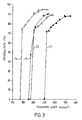
- the C1 crystallinity curve ( Figure 3) shows the presence of a very marked crystallization threshold at around 255 mJ / cm2. This is in fact the energy threshold necessary for the partial melting of the layer of amorphous silicon at room temperature. Below this threshold, the entire layer of silicon appears partially crystallized. The rate of crystallization gradually increases until energies are sufficient for the entire layer to melt. This development should be linked to the description of the process made previously.
- the optimum treatment is reached when the crystallinity level measured by spectroscopic ellipsometry is maximum, here 350 mJ / cm 2 . This optimum corresponds to the best fit of the model to a single homogeneous layer, in the example chosen.
- the samples include an antireflective layer of silica with a thickness of the order of 55 nanometers, deposited on the layer of amorphous silicon.
- the optimization process is carried out in the same manner as above, and the energy range chosen is lower due to the presence of the anti-reflective layer.
- the same type of analysis after laser impact gives a crystallinity curve similar to the previous one, but very clearly shifted towards low energies.
- the optimum energy is reduced to around 260 mJ / cm 2 , which corresponds to the energy gain introduced by simple optical effect.
- the actual annealing control can to be placed.
- the laser impact repetition period is 6s and a 40 x 30 cm panel is treated in 9 pulses, or a processing capacity of the order of 50 panels at the hour, for the times indicated.
- the process described not only improves the quality and reliability of laser annealing of amorphous silicon, but also to control the deposit stage of the amorphous silicon whose homogeneity is not always perfect.
- step a) an ellipsometry measurement is carried out on each area to be treated on the panel, in order to obtain the multiplet of physico-chemical characteristics of the area of each area to be treated, while in step b) the determination of the energy of the laser beam necessary for processing is performed based on all bytes characteristics obtained in step a).
- the positioning includes a sub-step d1) in which an ellipsometry measurement is carried out on the area, in order to adjust its positioning according to direction Z.
- steps d) and e) there is provided a intermediate stage of) in which the energy of the laser required for surface treatment of the area, function of the energy determined in step b), of the adjustment in position performed in sub-step dl) and from the table of correspondence.
- steps c) and d provides for a sub-step c ') in which a ellipsometry measurement of the treated surface, in order to determine the new characteristics of the multiplet.
Landscapes
- Engineering & Computer Science (AREA)
- Mechanical Engineering (AREA)
- Recrystallisation Techniques (AREA)
- Removal Of Insulation Or Armoring From Wires Or Cables (AREA)
- Internal Circuitry In Semiconductor Integrated Circuit Devices (AREA)
- Encapsulation Of And Coatings For Semiconductor Or Solid State Devices (AREA)
- Drying Of Semiconductors (AREA)
- Length Measuring Devices By Optical Means (AREA)
- Laser Beam Processing (AREA)
Claims (12)
- Verfahren zur Oberflächenbearbeitung mit Laser,
wobei eine Reihe von mindestens zwei getrennten, in physikalisch-chemischer Hinsicht im Wesentlichen gleichartigen Bereichen zur Verfügung steht, die jeweils eine Siliziumschicht mit einer bestimmten Tiefe umfassen, und wobei auf jede einmalig oder mehrmalig ein Laserstrahl von ausgewählter Energie angewendet wird, um die Siliziumschicht der Bereiche zu rekristallisieren,
dadurch gekennzeichnet, dass
es die folgenden Schritte umfasst:a) Vornehmen von mindestens einer Ellipsometriemessung am ersten Bereich vor mindestens einer Anwendung des Laserstrahls an dem ersten Bereich, um ein Multiplett physikalisch-chemischer Eigenschaften des ersten Bereichs zu erhalten,b) Bestimmen der Energie des Laserstrahls, die zur Rekristallisierung der Siliziumschicht des ersten Bereichs notwendig ist, in Abhängigkeit von zumindest dem Multiplett von Eigenschaften, das in Schritt a) erhalten wurde, und einer gespeicherten Zuordnungstabelle,c) Beaufschlagen des ersten Bereichs mit mindestens einem Laserbeschuss mit der in Schritt b) bestimmten Energie,d) Positionieren des zweiten Bereichs im Hinblick auf den Laserstrahl, unde) Beaufschlagen des zweiten Bereichs mit mindestens einem Laserbeschuss mit der in Schritt b) bestimmten Energie, wodurch der Rekristallisierungsprozess des Siliziums mittels Laser an der Reihe von Bereichen optimiert werden kann, wobei das Anwenden der Laserenergie mittels der Ellipsometriemessung gesteuert wird. - Verfahren nach Anspruch 1,
dadurch gekennzeichnet, dass
in Schritt a) eine Ellipsometriemessung mindestens auch am zweiten zu bearbeitenden Bereich durchgeführt wird, um das Multiplett von physikalisch-chemischen Eigenschaften der Oberfläche des ersten und zweiten zu bearbeitenden Bereichs zu erhalten, und wobei in Schritt b) die Bestimmung der Energie des zur Bearbeitung notwendigen Laserstrahls in Abhängigkeit von allen Multipletten von Eigenschaften vorgenommen wird, die in Schritt a) erhalten wurden. - Verfahren nach Anspruch 1,
dadurch gekennzeichnet, dass
zwischen den Schritten d) und e) ein Zwischenschritt d') vorgesehen ist, bei dem die zur Oberflächenbearbeitung des zweiten Bereichs notwendige Laserenergie in Abhängigkeit von der in Schritt b) bestimmten Energie und der Zuordnungstabelle eingestellt wird. - Verfahren nach Anspruch 1,
wobei der erste Bereich in einer Ausgangsposition festgesetzt wird, die durch drei Koordinaten bezüglich eines orthonormierten Bezugssystems (X, Y, Z) bestimmt ist,
dadurch gekennzeichnet, dass
in Schritt d) die Positionierung des zweiten Bereichs eine Verschiebung des zweiten Bereichs in der X-Y-Ebene umfasst. - Verfahren nach Anspruch 4,
dadurch gekennzeichnet, dass
in Schritt d) die Positionierung des zweiten Bereichs darüber hinaus einen Teilschritt d1) umfasst, wobei eine Ellipsometriemessung am zweiten Bereich vorgenommen wird, um dessen Positionierung in der Z-Richtung einzustellen. - Verfahren nach Anspruch 5,
dadurch gekennzeichnet, dass
die Einstellung der für die Oberflächenbearbeitung des zweiten Bereichs notwendigen Energie des Lasers in Abhängigkeit von der in Schritt b) bestimmten Energie, von der im Teilschritt d1) vorgenommenen Positionseinstellung und von der Zuordnungstabelle durchgeführt wird. - Verfahren nach einem der Ansprüche 1 bis 6,
dadurch gekennzeichnet, dass
zwischen den Schritten c) und d) ein Teilschritt c') vorgesehen ist, in dem eine Ellipsometriemessung des ersten Bereichs vorgenommen wird, um die neuen Eigenschaften des Multipletts zu bestimmen. - Verfahren nach einem der vorhergehenden Ansprüche,
dadurch gekennzeichnet, dass
die Ellipsometriemessung spektroskopisch ist. - Verfahren nach einem der Ansprüche 1 bis 7,
dadurch gekennzeichnet, dass
die Ellipsometriemessung bei einer oder mehreren Wellenlängen vorgenommen wird. - Verfahren nach einem der Ansprüche 1 bis 9,
dadurch gekennzeichnet, dass
die physikalisch-chemische Charakterisierung von jedem Bereich durch Ellipsometrie die Messung mindestens eines Parameters umfasst, der zur Gruppe gehört, die aus der Dicke dieses Bereichs, der Dichte und dem optischen Index dieses Bereichs, der Dicke der verschiedenen, auf diesem Bereich vorhandenen Schichten und der physikalisch-chemischen Zusammensetzung dieses Bereichs besteht. - Verfahren nach einem der vorhergehenden Ansprüche,
dadurch gekennzeichnet, dass
jeder zu bearbeitende Bereich auf einer Schicht aus amorphem Silizium, die auf einem Glassubstrat abgeschieden ist, eine darüber liegende Schicht umfasst, die aus einem Material besteht, das optische Entspiegelungseigenschaften aufweist, die auf der oberen Seite der Schicht aus amorphem Silizium, dem Substrat gegenüber liegend, abgeschieden ist. - Vorrichtung zur Oberflächenbearbeitung mittels Laser zum Durchführen des Verfahrens nach einem der vorhergehenden Ansprüche,
dadurch gekennzeichnet, dass
die Vorrichtung Folgendes aufweist:ein Ellipsometer (EL), das sich dazu eignet, vor mindestens einem der Anlegevorgänge des Laserstrahls auf den ersten Bereich mindestens eine Ellipsometriemessung am ersten Bereich vorzunehmen, um ein Multiplett von physikalisch-chemischen Eigenschaften des ersten Bereichs zu erhalten,Berechnungseinrichtungen (GES1, GES2), um die zur Rekristallisierung der Siliziumschicht des ersten Bereichs notwendige Energie des Laserstrahls in Abhängigkeit von zumindest dem auf diese Weise erhaltenen Multiplett von Eigenschaften und einer gespeicherten Zuordnungstabelle zu bestimmen,Einrichtungen (LA), um den ersten Bereich mit mindestens einem Laserbeschuss mit der von den Berechnungseinrichtungen auf diese Weise bestimmten Energie zu beaufschlagen,Einrichtungen (TAB), um den nächsten Bereich im Hinblick auf den Laserstrahl zu positionieren, wobei sich die Einrichtungen (LA) dazu eignen, den zweiten Bereich mit mindestens einem Laserbeschuss mit der durch die Berechnungseinrichtungen am ersten Bereich bestimmten Energie zu beaufschlagen.
Applications Claiming Priority (3)
| Application Number | Priority Date | Filing Date | Title |
|---|---|---|---|
| FR9509778 | 1995-08-11 | ||
| FR9509778A FR2737806B1 (fr) | 1995-08-11 | 1995-08-11 | Dispositif et procede de traitement de surface par laser |
| PCT/FR1996/001034 WO1997007539A1 (fr) | 1995-08-11 | 1996-07-03 | Dispositif et procede de traitement de surface par laser |
Publications (2)
| Publication Number | Publication Date |
|---|---|
| EP0843889A1 EP0843889A1 (de) | 1998-05-27 |
| EP0843889B1 true EP0843889B1 (de) | 2004-09-29 |
Family
ID=9481898
Family Applications (1)
| Application Number | Title | Priority Date | Filing Date |
|---|---|---|---|
| EP96924926A Expired - Lifetime EP0843889B1 (de) | 1995-08-11 | 1996-07-03 | Vorrichtung und verfahren zur laser-oberflächenbehandlung |
Country Status (9)
| Country | Link |
|---|---|
| US (1) | US6073464A (de) |
| EP (1) | EP0843889B1 (de) |
| JP (1) | JP3996641B2 (de) |
| KR (1) | KR100403792B1 (de) |
| AT (1) | ATE278250T1 (de) |
| CA (1) | CA2225422C (de) |
| DE (1) | DE69633511T2 (de) |
| FR (1) | FR2737806B1 (de) |
| WO (1) | WO1997007539A1 (de) |
Families Citing this family (20)
| Publication number | Priority date | Publication date | Assignee | Title |
|---|---|---|---|---|
| FR2737786B1 (fr) * | 1995-08-11 | 1997-09-12 | Soc D Production Et De Rech Ap | Dispositif optique pour homogeneiser un faisceau laser |
| FR2737814B1 (fr) * | 1995-08-11 | 1997-09-12 | Soc D Production Et De Rech Ap | Procede et dispositif de commande d'une source laser a plusieurs modules laser pour optimiser le traitement de surface par laser |
| TW444275B (en) * | 1998-01-13 | 2001-07-01 | Toshiba Corp | Processing device, laser annealing device, laser annealing method, manufacturing device and substrate manufacturing device for panel display |
| KR100322135B1 (ko) * | 1999-03-11 | 2002-02-04 | 윤종용 | 잔류 기계적 스트레스를 최대화하는 광섬유 및 이를 이용한 광섬유 격자 제작방법 |
| JP3447654B2 (ja) * | 2000-03-24 | 2003-09-16 | Necエレクトロニクス株式会社 | 異方性薄膜評価法及び評価装置 |
| US20030119060A1 (en) * | 2001-08-10 | 2003-06-26 | Desrosiers Peter J. | Apparatuses and methods for creating and testing pre-formulations and systems for same |
| TW586173B (en) * | 2002-11-29 | 2004-05-01 | Au Optronics Corp | Method of monitoring a laser crystallization process |
| TWI284443B (en) * | 2003-01-07 | 2007-07-21 | Au Optronics Corp | Automatic control system and method of laser energy |
| WO2005036627A1 (en) * | 2003-10-03 | 2005-04-21 | Applied Materials, Inc. | Absorber layer for dynamic surface annealing processing |
| US7109087B2 (en) * | 2003-10-03 | 2006-09-19 | Applied Materials, Inc. | Absorber layer for DSA processing |
| JP2006040949A (ja) * | 2004-07-22 | 2006-02-09 | Advanced Lcd Technologies Development Center Co Ltd | レーザー結晶化装置及びレーザー結晶化方法 |
| JP2006088163A (ja) * | 2004-09-21 | 2006-04-06 | Fanuc Ltd | レーザ装置 |
| US7796260B1 (en) * | 2006-04-25 | 2010-09-14 | J.A. Woollam Co., Inc. | System and method of controlling intensity of an electromagnetic beam |
| KR20100105606A (ko) * | 2007-11-21 | 2010-09-29 | 더 트러스티이스 오브 콜롬비아 유니버시티 인 더 시티 오브 뉴욕 | 에피택셜하게 텍스쳐화된 후막의 제조를 위한 시스템 및 방법 |
| EP2470485A4 (de) * | 2009-08-27 | 2012-12-26 | Mcalister Technologies Llc | Keramikisolator sowie herstellungsverfahren und verwendungsverfahren dafür |
| US8994943B2 (en) * | 2012-11-30 | 2015-03-31 | Infineon Technologies Ag | Selectivity by polarization |
| JP6348149B2 (ja) * | 2016-07-08 | 2018-06-27 | ファナック株式会社 | ロボットを用いてレーザ加工を行うレーザ加工ロボットシステム |
| JP6464213B2 (ja) * | 2017-02-09 | 2019-02-06 | ファナック株式会社 | レーザ加工ヘッドおよび撮影装置を備えるレーザ加工システム |
| FR3075377B1 (fr) * | 2017-12-19 | 2020-10-16 | Commissariat Energie Atomique | Procede de caracterisation et de controle de l'homogeneite de pieces metalliques fabriquees par frittage laser |
| GB2571997B (en) | 2018-03-16 | 2021-10-27 | X Fab Texas Inc | Use of wafer brightness to monitor laser anneal process and laser anneal tool |
Family Cites Families (13)
| Publication number | Priority date | Publication date | Assignee | Title |
|---|---|---|---|---|
| JPS59168636A (ja) * | 1983-03-15 | 1984-09-22 | Toshiba Corp | ド−ズ量評価方法 |
| US4897154A (en) * | 1986-07-03 | 1990-01-30 | International Business Machines Corporation | Post dry-etch cleaning method for restoring wafer properties |
| US4962065A (en) * | 1989-02-13 | 1990-10-09 | The University Of Arkansas | Annealing process to stabilize PECVD silicon nitride for application as the gate dielectric in MOS devices |
| JPH03295251A (ja) * | 1990-04-12 | 1991-12-26 | Sumitomo Electric Ind Ltd | 半導体基板の表面状態検査方法 |
| US5313044A (en) * | 1992-04-28 | 1994-05-17 | Duke University | Method and apparatus for real-time wafer temperature and thin film growth measurement and control in a lamp-heated rapid thermal processor |
| JPH06288835A (ja) * | 1993-03-30 | 1994-10-18 | Shimadzu Corp | エリプソメータ |
| US5399229A (en) * | 1993-05-13 | 1995-03-21 | Texas Instruments Incorporated | System and method for monitoring and evaluating semiconductor wafer fabrication |
| KR100306527B1 (ko) * | 1994-06-15 | 2002-06-26 | 구사마 사부로 | 박막반도체장치의제조방법,박막반도체장치 |
| FR2737814B1 (fr) * | 1995-08-11 | 1997-09-12 | Soc D Production Et De Rech Ap | Procede et dispositif de commande d'une source laser a plusieurs modules laser pour optimiser le traitement de surface par laser |
| FR2737779B1 (fr) * | 1995-08-11 | 1997-09-12 | Soc D Production Et De Rech Ap | Dispositif ellipsometre a haute resolution spatiale |
| FR2737786B1 (fr) * | 1995-08-11 | 1997-09-12 | Soc D Production Et De Rech Ap | Dispositif optique pour homogeneiser un faisceau laser |
| US5798837A (en) * | 1997-07-11 | 1998-08-25 | Therma-Wave, Inc. | Thin film optical measurement system and method with calibrating ellipsometer |
| US5864393A (en) * | 1997-07-30 | 1999-01-26 | Brown University Research Foundation | Optical method for the determination of stress in thin films |
-
1995
- 1995-08-11 FR FR9509778A patent/FR2737806B1/fr not_active Expired - Fee Related
-
1996
- 1996-07-03 EP EP96924926A patent/EP0843889B1/de not_active Expired - Lifetime
- 1996-07-03 DE DE69633511T patent/DE69633511T2/de not_active Expired - Fee Related
- 1996-07-03 JP JP50897997A patent/JP3996641B2/ja not_active Expired - Fee Related
- 1996-07-03 WO PCT/FR1996/001034 patent/WO1997007539A1/fr not_active Ceased
- 1996-07-03 KR KR10-1998-0700915A patent/KR100403792B1/ko not_active Expired - Fee Related
- 1996-07-03 US US09/000,126 patent/US6073464A/en not_active Expired - Lifetime
- 1996-07-03 CA CA002225422A patent/CA2225422C/en not_active Expired - Fee Related
- 1996-07-03 AT AT96924926T patent/ATE278250T1/de not_active IP Right Cessation
Also Published As
| Publication number | Publication date |
|---|---|
| CA2225422C (en) | 2007-05-22 |
| DE69633511T2 (de) | 2005-11-17 |
| EP0843889A1 (de) | 1998-05-27 |
| DE69633511D1 (de) | 2004-11-04 |
| FR2737806B1 (fr) | 1997-09-12 |
| KR100403792B1 (ko) | 2004-03-24 |
| ATE278250T1 (de) | 2004-10-15 |
| US6073464A (en) | 2000-06-13 |
| JP3996641B2 (ja) | 2007-10-24 |
| JPH11510960A (ja) | 1999-09-21 |
| FR2737806A1 (fr) | 1997-02-14 |
| KR19990036247A (ko) | 1999-05-25 |
| WO1997007539A1 (fr) | 1997-02-27 |
| CA2225422A1 (en) | 1997-02-27 |
Similar Documents
| Publication | Publication Date | Title |
|---|---|---|
| EP0843889B1 (de) | Vorrichtung und verfahren zur laser-oberflächenbehandlung | |
| EP3036352B1 (de) | Verfahren zur herstellung eines substrats mit einer beschichtung mit einer diskontinuierlichen dünnen metallschicht | |
| CA2922526C (fr) | Dispositif et procede de marquage laser d'une lentille ophtalmique avec un laser pulse de longueur d'onde et energie par impulsion selectionnees | |
| EP0191661B1 (de) | Verfahren zur Erzeugung und Kristallisation einer dünnen Schicht eines organischen Materials mit einem Energiestrahl | |
| US20070002308A1 (en) | Method of and apparatus for in-situ monitoring of crystallization state | |
| EP3475742B1 (de) | Verfahren und systeme zur optischen funktionalisierung einer probe aus halbleitermaterial | |
| FR3031197A1 (fr) | Procede de traitement thermique rapide d'un empilement electrochrome tout solide complet | |
| EP2661612A1 (de) | Vorrichtung zur bildung eines interferenzgitters auf einer probe | |
| EP0045551A1 (de) | Verfahren zur Herstellung polykristalliner Filme aus Halbleitern, die aus einer Verbindung oder einem Element bestehen, und dabei erhaltene Filme | |
| EP0843811B1 (de) | Ellipsometer mit hoher räumlicher auflösung | |
| FR2737814A1 (fr) | Procede et dispositif de commande d'une source laser a plusieurs modules laser pour optimiser le traitement de surface par laser | |
| EP0466598B1 (de) | Verfahren und Einrichtung zur Ablagerung von Antireflektionsschichten und zur Kontrolle ihrer Dicke | |
| EP2817664A1 (de) | Optische reflektierende diffraktionsvorrichtung mit hoher beständigkeit gegen laserfluss | |
| US7542152B2 (en) | Method for measuring thickness of thin film, method for forming polycrystal semiconductor thin film, method for manufacturing semiconductor device, apparatus for manufacturing the same, and method for manufacturing image display device | |
| TW201105949A (en) | Measurement of thin film photovoltaic solar panels | |
| Arnone et al. | Study of Photo-Induced Thin Film Growth on Cds Substrates. | |
| FR2850461A1 (fr) | Procede et appareil pour realiser un substrat pour semi-conducteur ou similaire | |
| FR3002687A1 (fr) | Procede de traitement d une structure | |
| FR3073839B1 (fr) | Systeme d’alignement d’un dispositif de traitement thermique et son fonctionnement | |
| JP5347122B2 (ja) | 結晶化率の測定方法及び測定装置 | |
| FR3133514A1 (fr) | Procédé de correction d’épaisseur d’une couche piézoélectrique | |
| Ghica et al. | High-optical-quality LiNbO3 thin films obtained by pulsed laser deposition | |
| FR2634566A1 (fr) | Procede et dispositif pour figer l'image d'un champ electrique dans un materiau | |
| EP0923121A1 (de) | Verfahren zur Herstellung von Dünnschichtvorrichtungen unter Verwendung der anisotropen Reflektionstechnik | |
| WO2012052373A1 (fr) | Methode de determination de la transmission opto-energetique d'un materiau transparent ou translucide et dispositif pour sa mise en oeuvre |
Legal Events
| Date | Code | Title | Description |
|---|---|---|---|
| PUAI | Public reference made under article 153(3) epc to a published international application that has entered the european phase |
Free format text: ORIGINAL CODE: 0009012 |
|
| 17P | Request for examination filed |
Effective date: 19971215 |
|
| AK | Designated contracting states |
Kind code of ref document: A1 Designated state(s): AT BE CH DE DK ES FI FR GB GR IE IT LI LU MC NL PT SE |
|
| 17Q | First examination report despatched |
Effective date: 19991202 |
|
| GRAP | Despatch of communication of intention to grant a patent |
Free format text: ORIGINAL CODE: EPIDOSNIGR1 |
|
| GRAS | Grant fee paid |
Free format text: ORIGINAL CODE: EPIDOSNIGR3 |
|
| GRAA | (expected) grant |
Free format text: ORIGINAL CODE: 0009210 |
|
| AK | Designated contracting states |
Kind code of ref document: B1 Designated state(s): AT BE CH DE DK ES FI FR GB GR IE IT LI LU MC NL PT SE |
|
| PG25 | Lapsed in a contracting state [announced via postgrant information from national office to epo] |
Ref country code: FI Free format text: LAPSE BECAUSE OF FAILURE TO SUBMIT A TRANSLATION OF THE DESCRIPTION OR TO PAY THE FEE WITHIN THE PRESCRIBED TIME-LIMIT Effective date: 20040929 |
|
| REG | Reference to a national code |
Ref country code: GB Ref legal event code: FG4D Free format text: NOT ENGLISH |
|
| REG | Reference to a national code |
Ref country code: CH Ref legal event code: EP |
|
| REG | Reference to a national code |
Ref country code: IE Ref legal event code: FG4D Free format text: FRENCH |
|
| REF | Corresponds to: |
Ref document number: 69633511 Country of ref document: DE Date of ref document: 20041104 Kind code of ref document: P |
|
| PG25 | Lapsed in a contracting state [announced via postgrant information from national office to epo] |
Ref country code: SE Free format text: LAPSE BECAUSE OF FAILURE TO SUBMIT A TRANSLATION OF THE DESCRIPTION OR TO PAY THE FEE WITHIN THE PRESCRIBED TIME-LIMIT Effective date: 20041229 Ref country code: GR Free format text: LAPSE BECAUSE OF FAILURE TO SUBMIT A TRANSLATION OF THE DESCRIPTION OR TO PAY THE FEE WITHIN THE PRESCRIBED TIME-LIMIT Effective date: 20041229 Ref country code: DK Free format text: LAPSE BECAUSE OF FAILURE TO SUBMIT A TRANSLATION OF THE DESCRIPTION OR TO PAY THE FEE WITHIN THE PRESCRIBED TIME-LIMIT Effective date: 20041229 |
|
| PG25 | Lapsed in a contracting state [announced via postgrant information from national office to epo] |
Ref country code: ES Free format text: LAPSE BECAUSE OF FAILURE TO SUBMIT A TRANSLATION OF THE DESCRIPTION OR TO PAY THE FEE WITHIN THE PRESCRIBED TIME-LIMIT Effective date: 20050109 |
|
| GBT | Gb: translation of ep patent filed (gb section 77(6)(a)/1977) | ||
| PG25 | Lapsed in a contracting state [announced via postgrant information from national office to epo] |
Ref country code: LU Free format text: LAPSE BECAUSE OF NON-PAYMENT OF DUE FEES Effective date: 20050703 |
|
| PGFP | Annual fee paid to national office [announced via postgrant information from national office to epo] |
Ref country code: GB Payment date: 20050721 Year of fee payment: 10 |
|
| PGFP | Annual fee paid to national office [announced via postgrant information from national office to epo] |
Ref country code: IE Payment date: 20050728 Year of fee payment: 10 |
|
| PGFP | Annual fee paid to national office [announced via postgrant information from national office to epo] |
Ref country code: NL Payment date: 20050730 Year of fee payment: 10 |
|
| PG25 | Lapsed in a contracting state [announced via postgrant information from national office to epo] |
Ref country code: MC Free format text: LAPSE BECAUSE OF NON-PAYMENT OF DUE FEES Effective date: 20050731 Ref country code: LI Free format text: LAPSE BECAUSE OF NON-PAYMENT OF DUE FEES Effective date: 20050731 Ref country code: CH Free format text: LAPSE BECAUSE OF NON-PAYMENT OF DUE FEES Effective date: 20050731 |
|
| PGFP | Annual fee paid to national office [announced via postgrant information from national office to epo] |
Ref country code: AT Payment date: 20050803 Year of fee payment: 10 |
|
| PLBE | No opposition filed within time limit |
Free format text: ORIGINAL CODE: 0009261 |
|
| STAA | Information on the status of an ep patent application or granted ep patent |
Free format text: STATUS: NO OPPOSITION FILED WITHIN TIME LIMIT |
|
| PGFP | Annual fee paid to national office [announced via postgrant information from national office to epo] |
Ref country code: BE Payment date: 20050824 Year of fee payment: 10 |
|
| 26N | No opposition filed |
Effective date: 20050630 |
|
| REG | Reference to a national code |
Ref country code: CH Ref legal event code: PL |
|
| PG25 | Lapsed in a contracting state [announced via postgrant information from national office to epo] |
Ref country code: IE Free format text: LAPSE BECAUSE OF NON-PAYMENT OF DUE FEES Effective date: 20060703 Ref country code: GB Free format text: LAPSE BECAUSE OF NON-PAYMENT OF DUE FEES Effective date: 20060703 Ref country code: AT Free format text: LAPSE BECAUSE OF NON-PAYMENT OF DUE FEES Effective date: 20060703 |
|
| PG25 | Lapsed in a contracting state [announced via postgrant information from national office to epo] |
Ref country code: BE Free format text: LAPSE BECAUSE OF NON-PAYMENT OF DUE FEES Effective date: 20060731 |
|
| PG25 | Lapsed in a contracting state [announced via postgrant information from national office to epo] |
Ref country code: NL Free format text: LAPSE BECAUSE OF NON-PAYMENT OF DUE FEES Effective date: 20070201 |
|
| GBPC | Gb: european patent ceased through non-payment of renewal fee |
Effective date: 20060703 |
|
| NLV4 | Nl: lapsed or anulled due to non-payment of the annual fee |
Effective date: 20070201 |
|
| REG | Reference to a national code |
Ref country code: IE Ref legal event code: MM4A |
|
| BERE | Be: lapsed |
Owner name: SOC. DE PRODUCTION ET DE *RECHERCHES APPLIQUEES Effective date: 20060731 |
|
| PG25 | Lapsed in a contracting state [announced via postgrant information from national office to epo] |
Ref country code: PT Free format text: LAPSE BECAUSE OF NON-PAYMENT OF DUE FEES Effective date: 20050228 |
|
| PGFP | Annual fee paid to national office [announced via postgrant information from national office to epo] |
Ref country code: DE Payment date: 20080829 Year of fee payment: 13 |
|
| PGFP | Annual fee paid to national office [announced via postgrant information from national office to epo] |
Ref country code: IT Payment date: 20080726 Year of fee payment: 13 Ref country code: FR Payment date: 20080729 Year of fee payment: 13 |
|
| REG | Reference to a national code |
Ref country code: FR Ref legal event code: ST Effective date: 20100331 |
|
| PG25 | Lapsed in a contracting state [announced via postgrant information from national office to epo] |
Ref country code: FR Free format text: LAPSE BECAUSE OF NON-PAYMENT OF DUE FEES Effective date: 20090731 |
|
| PG25 | Lapsed in a contracting state [announced via postgrant information from national office to epo] |
Ref country code: DE Free format text: LAPSE BECAUSE OF NON-PAYMENT OF DUE FEES Effective date: 20100202 |
|
| PG25 | Lapsed in a contracting state [announced via postgrant information from national office to epo] |
Ref country code: IT Free format text: LAPSE BECAUSE OF NON-PAYMENT OF DUE FEES Effective date: 20090703 |
|
| P01 | Opt-out of the competence of the unified patent court (upc) registered |
Effective date: 20230525 |