EP0841728B1 - Fassung für elektrische und elektronische Komponenten - Google Patents
Fassung für elektrische und elektronische Komponenten Download PDFInfo
- Publication number
- EP0841728B1 EP0841728B1 EP97119037A EP97119037A EP0841728B1 EP 0841728 B1 EP0841728 B1 EP 0841728B1 EP 97119037 A EP97119037 A EP 97119037A EP 97119037 A EP97119037 A EP 97119037A EP 0841728 B1 EP0841728 B1 EP 0841728B1
- Authority
- EP
- European Patent Office
- Prior art keywords
- socket
- cap
- contact
- component
- chamber
- Prior art date
- Legal status (The legal status is an assumption and is not a legal conclusion. Google has not performed a legal analysis and makes no representation as to the accuracy of the status listed.)
- Expired - Lifetime
Links
Images


Classifications
-
- H—ELECTRICITY
- H01—ELECTRIC ELEMENTS
- H01G—CAPACITORS; CAPACITORS, RECTIFIERS, DETECTORS, SWITCHING DEVICES, LIGHT-SENSITIVE OR TEMPERATURE-SENSITIVE DEVICES OF THE ELECTROLYTIC TYPE
- H01G2/00—Details of capacitors not covered by a single one of groups H01G4/00-H01G11/00
- H01G2/02—Mountings
- H01G2/04—Mountings specially adapted for mounting on a chassis
-
- H—ELECTRICITY
- H01—ELECTRIC ELEMENTS
- H01R—ELECTRICALLY-CONDUCTIVE CONNECTIONS; STRUCTURAL ASSOCIATIONS OF A PLURALITY OF MUTUALLY-INSULATED ELECTRICAL CONNECTING ELEMENTS; COUPLING DEVICES; CURRENT COLLECTORS
- H01R13/00—Details of coupling devices of the kinds covered by groups H01R12/70 or H01R24/00 - H01R33/00
- H01R13/46—Bases; Cases
- H01R13/514—Bases; Cases composed as a modular blocks or assembly, i.e. composed of co-operating parts provided with contact members or holding contact members between them
-
- H—ELECTRICITY
- H01—ELECTRIC ELEMENTS
- H01R—ELECTRICALLY-CONDUCTIVE CONNECTIONS; STRUCTURAL ASSOCIATIONS OF A PLURALITY OF MUTUALLY-INSULATED ELECTRICAL CONNECTING ELEMENTS; COUPLING DEVICES; CURRENT COLLECTORS
- H01R13/00—Details of coupling devices of the kinds covered by groups H01R12/70 or H01R24/00 - H01R33/00
- H01R13/66—Structural association with built-in electrical component
- H01R13/6608—Structural association with built-in electrical component with built-in single component
-
- H—ELECTRICITY
- H05—ELECTRIC TECHNIQUES NOT OTHERWISE PROVIDED FOR
- H05K—PRINTED CIRCUITS; CASINGS OR CONSTRUCTIONAL DETAILS OF ELECTRIC APPARATUS; MANUFACTURE OF ASSEMBLAGES OF ELECTRICAL COMPONENTS
- H05K3/00—Apparatus or processes for manufacturing printed circuits
- H05K3/30—Assembling printed circuits with electric components, e.g. with resistors
- H05K3/301—Assembling printed circuits with electric components, e.g. with resistors by means of a mounting structure
Definitions
- the invention relates to a socket for electrical and electronic components other than illuminants according to claim 1, an arrangement of several such Sockets according to claim 17 and a method for fixing and contacting an electrical or electronic Component within such a version according to claim 18.
- Electrical components are known to be on a PCB mounted by placing it on defined locations the surface of the circuit board glued or with their Pins inserted in contacted holes and with these are soldered. Assembled this way electrical components, in particular photodiodes or However, photo transistors can no longer be positioned correct.
- US-A-5,118,308 is a multi-part bus connector known with a base part in which several slots are provided by the fork-shaped connection contacts can be put through.
- the connection contacts protrude in the inserted state with its fork-shaped sections out of the slots.
- An upper housing part has other, several resistance chambers, in the resistors that lock a bus that can be used.
- the top Housing part also has several grooves for receiving Connecting wires of the resistors. Are the base part and the upper part of the housing put together, they grip Connection wires of the resistors in the fork-shaped Sections of the contacts and are thereby in held the grooves.
- the Component connection clamping device has a first and second part with suitable contact surfaces and Engagement elements on the in the assembled state Keep surfaces of parts in contact.
- the surface of the first and second part faces each next two channels for receiving one conductor and one Cavity on, which is an electrical component with itself axially extending contact wires can accommodate.
- In the second Part are two spaced apart Contact elements arranged such that the in the cavity component used across the in the channels arranged conductors with assembled Connection clamping device is switched.
- a feed and Holding component for electrical components for electrical components, e.g. Microlamps, known.
- the component comprises a housing, in which such a micro lamp can be used.
- the Bottom part of the housing forms a slot through which the Lead wires of the micro lamp led out of the housing become.
- Coupling seats are located outside the housing Inclusion of electrical resistors is provided corresponding connecting conductor and one of the Contact the micro lamp lead wires.
- DE OS 2310151 discloses a version for socketless small electric lamps that have a housing with a Plug-in space for the glass bulb of an electrical Small lamp has. Housing slots that run across the Direction of insertion of the glass bulb extend in the insertion space. Contact flags protrude with one end out the case and the other end through the Housing slots in the insertion space. From the Glass bulbs protrude lead wires that when inserted the glass bulb in the insertion space in the direction of insertion Glass bulb to be bent. Come in the inserted state the ends of the contact tabs in contact with the insertion space the lead wires of the glass bulb.
- From DE-U-7614462 is a jack for receiving the connections of separate components known.
- the Multiple socket contacts, each with are covered by a hollow cap. When inserting one Component then come the pin contacts within each cap in contact with the socket contacts.
- the invention is based on the object of making a base, more precisely a socket for electrical and electronic components, which can be produced inexpensively and can also be assembled on site by the customer with little effort, with an inserted component in relation can be positioned on the socket.
- the version according to the invention is used in particular mechanical stabilization, a defined Positioning an electrical or electronic Component as well as the reliable electrical connection.
- the component is, for example, a electrical resistance, a coil a capacitor, a Transistor, a diode, etc.
- the one- piece socket has one or more caps for receiving at least one predetermined, at least one contact part of an electrical or electronic component, the cap being dimensioned such that manufacturing-related tolerances of the component can be compensated.
- Each cap is assigned at least one chamber for receiving a contact element, the contact element being designed such that it forms an electrically conductive press connection with the connection contact within the chamber in the inserted state.
- a first hole leads from the cap into the chamber, through which the connection contact, which is advantageous an electrode wire when inserting the component is put through.
- connection contact which is advantageous an electrode wire when inserting the component is put through.
- tapered the cross-sectional area of the cap in the direction of insertion Component.
- the contact receiving chamber runs with respect to the direction of insertion of the component expediently at right angles and is located behind the cap.
- the chamber can be designed as a passage, or only runs partly by the version.
- the distance between the Holes are dimensioned so that during the pressing forces of the contact element essentially of included in the version and not routed into the component become. This creates a form-fitting Connection which ensures that the electrode wire and so that the component also with mechanical shocks, which, for example, during an operation in Motor vehicles occur, is kept safe.
- the second Hole also acts as an anvil when out of the socket protruding section of the lead wire cut off becomes.
- To insert the contact element against one To protect canting and a friction between the To avoid contact element and the chamber essentially has these guide grooves and / or guide grooves that run at least partially in the chamber.
- the Contact element itself has projections that at least in the inserted state with the respective guide grooves work together.
- the protrusions can be Act expressions through corresponding impressions on the opposite side of the contact element are caused.
- the contact element is preferably around a contact pin that at one end in two Contact legs expires with the inserted state the connection contact of the component a press connection form.
- the contact element has locking projections which in interact with the chamber in such a way that the contact element is held firmly in the chamber and against unwanted pulling out is protected.
- the Contact element can also be used as an insulation displacement contact be trained.
- the contact element with the terminal contact forms a press connection and the position of the component in relation to the socket or the contact element is a filling material, in particular a Permanently elastic adhesive sealing compound, through an opening in the Cap filled.
- the adhesive sealing compound can be a high temperature hot melt adhesive or around one by means of UV radiation act curable resin whose elastic property is expediently chosen so that vibrations and other external loads to the Component are damped. That is sufficient Protection of the component against vibrations and Vibrations possible.
- Holding, guiding and / or Locking devices for releasable connection to at least another version may be provided.
- the Versions next to each other or partially star-shaped be connected to each other.
- As connecting devices offer u. a. dovetail wedges and complementary shaped recordings.
- the holding, Guide and / or locking devices are of this type dimensioned that the sockets have sufficient play to each other to by manufacturing Tolerances caused tensions within an arrangement to be able to compensate.
- the version can also have several, in a defined position have mutually arranged caps, each one Chamber for inserting a contact element is assigned.
- each one Chamber for inserting a contact element is assigned.
- the version shows corresponding positioning pins or holes and / or one Guide groove.
- the special design of the version and the Contact element an automated assembly process allow.
- unskilled people even on the spot the version with an electrical or electronic component connect and contact and then this assembly Mount on a circuit board.
- the version described so far is for components with a diameter of 6 mm, for example.
- electronic components with a smaller diameter, for example, 3 mm are on the Inner surface of the cap in relation to the direction of insertion of the electronic component several parallel ribs arranged corresponding to the cross section of the cap downsize.
- the ribs are on the Molded inside surface of the cap.
- the frame is advantageously made in one piece made of a dielectric injection molding material. It can also other dielectric materials, such as. B. Thermosets can be used.
- the version has cutouts in which Can engage locking arms of the support device.
- locking arms can be provided on the socket be in corresponding recesses of the Intervene carrier device.
- Sockets is in claim 17 and a method for fixing and contacting at least one component in claim 18 circumscribed.
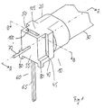
- Fig. 1 is a perspective view of a shown with 10 designated version.
- Version 10 has a cap 20 covering the receiving area for example for one end of an electrical Component such.
- B. a photodiode.
- On End portion of this photodiode 30 is shown in FIG. 1.
- the socket 10 also has a cap 20 subsequent rear part 40 in which a chamber 50th is arranged to receive a contact pin 60.
- a passage 50 is described as a chamber is, of course, it is conceivable, one only partially to provide through the rear portion 40 extending chamber.
- the passage 50 is perpendicular to the direction of insertion the photodiode 30.
- the photodiode 30 has one at each end Electrode or lead wire 70 on which in the assembled State with the contact pin 60 is an electrically conductive Press connection forms. As can be seen in Fig.1, are on the socket 10 centering pins 80 formed, the Mount the socket 10, for example on a Help make PCB easier.
- the Version also a guide groove 85, such as. B. in FIG. 7 indicated, be provided.
- the guide groove 85 also serves the assembly aid.
- the contact pin 60 is in this Embodiment inserted from below into the passage 50, i. H. from the side on which the centering pins 80 on the Version 10 are molded. This so-called insertion opening is designated 55.
- In the rear part 40 are laterally Except recesses 45 in the locking arms one Carrier device can intervene.
- 10 locking arms can be formed on the socket be in corresponding recesses on the Intervene carrier device.
- Fig. 2 shows a longitudinal section along the line A-A through the socket 10 according to FIG. 1.
- the cap 20 a in the direction of insertion of the photodiode 30, d. H. in Direction to the rear frame part 40, tapering Cross-sectional area.
- the cross-sectional area corresponds like that of a funnel.
- the funnel-shaped recording room the cap 20 opens into a hole 90, which in turn in the Passage 50 leads.
- the funnel-shaped taper Receiving space of the cap 20 facilitates the threading of the Connection wire 70 when sliding the socket 10 on the one end of the photodiode 30.
- In the rear wall 100, which delimits the passage 50 is also a hole 110 provided that is aligned with the hole 90 in the cap 20.
- the aligned holes or openings 90, 110 serve the connecting wire 70 of the photodiode 30th align and support.
- the distance between the two Openings 90, 110 should be selected such that the during the Inserting the contact pin 60 occurring forces in essentially not over the lead wire 70 in the Photodiode 30 are passed. That way ensures that when contacting the photodiode 30 none Damage to the contact points and the photodiode itself occurs.
- Fig. 3 is a cross section along the line B-B shown by the socket 20 shown in FIG. 1. in the 3 essentially shows the passage 50 of the holder 10 and the partially inserted contact pin 60.
- the Passage 50 has at least one boundary wall that is the rear wall 100 or the wall 105 that the Passage 50 connects to the cap 20, two guide grooves 120 on, parallel to the direction of insertion of the contact pin 60 run.
- the guide grooves 120 extend preferably not completely through the passage 50, but end at a certain distance before the Insertion opening 55 of the passage 50.
- the cross-sectional area The passage 50 is dimensioned such that it is in the area the insertion opening 55 is slightly wider than that Contact pin 60 itself and then in the direction of insertion Contact pin 60 widens so that the contact pin 60th can be pressed over the connecting wire 70.
- the contact pin 60 has an elongated pin 65, for example for Contacting the socket 10 is used with a circuit board.
- the pin 65 extends to a base region 160 which runs perpendicular to the elongated pin 65. From the base area 160 from two contact legs 130 and 135 extend parallel to the direction of insertion. At their outer end they are Contact legs 130 and 135 beveled and form a V-shaped Opening.
- the V-shaped opening opens into one of the two legs 130, 135 formed channel 170, the Inlet mouth is narrower than the diameter of the Lead 70.
- Towards elongated pin 65 The channel 170 widens to a size in the shape of a drop from about the diameter of the lead wire 70th corresponds.
- Each contact leg 130, 135 has one Bead 140 or 145, which when inserting the Contact pin 60 in the passage 50 with the respective Guide groove 120 cooperates to oppose the contact pin 60 protect a tilt and ensure that the Contact legs 130 and 135 can move freely so that the Contact pressure only insignificant due to friction between the Contact pin 60 and the passage 50 is affected.
- contact pin 60 At the Base part 160 of contact pin 60 are projections 150 in Form of locking hooks formed when inserting the Contact pin 60 in the walls of the passage 50 penetration. The inserted contact pin 60 is on this Way kept in the passage and against an unwanted Pull out protected.
- Fig. 3 shows also the hole 90 in the cap 20 through which the Lead wire 70 when applying the socket 10 on the Photodiode 30 is pushed through.
- Contact pin 60 contact pins of any shape for use can come that a press connection with the connecting wire 70 can manufacture.
- here is one Contact pin in insulation displacement technology is reminiscent.
- FIG. 4 is a front view of an alternative Embodiment of the socket 10 shown in FIG. 1 shown.
- “Front view” means in the entire description the view of the frame side, on which is used when inserting the photodiode 31 in the socket 11 would see.
- the socket 11 comprises two separate caps 21, which can be used to hold two photodiodes.
- everyone Cap 21 is a passage for receiving a contact pin 60 assigned. Version 11 otherwise corresponds to essentially the version shown in Fig. 10.
- Each Cap 21 has an oval cross-sectional area, the Main axis perpendicular to the longitudinal axis of contact pins 60 lies. The oval cross-sectional area not only enables an axial but also a lateral positioning of the Photodiode in the cap 21.
- the cap 21 can be any any, d. H. also rectangular or circular, Accept cross-sectional area.
- Version 11 can be part a connector can be used, for example two photodiodes with different sensitivity in one Install fiber optic system, the photodiodes depending on Can be controlled specifically.
- FIG. 5 is the front view of an alternative Version 12 shown, which has a single cap 22.
- the Cap 22 two passages (not shown) for receiving each assigned a contact pin 60 and has the Cap 20 two funnel-shaped depressions to the Passages 90 on.
- the passages are related to the Direction of insertion of a photodiode arranged side by side.
- the socket 12 can, for example, also have three passes Have recording each a contact pin.
- the version would include a Suitable for three-port phototransistors.
- each version shows Receiving devices 190 and complementary thereto Holding devices 200 on.
- This connection or Coupling devices advantageously have the shape a dovetail.
- the dovetail-shaped Connection devices 190, 200 are dimensioned such that the assembled versions sufficiently against each other can be moved to manufacturing-related To be able to compensate for inaccuracies in the socket body.
- Each socket has an inlet opening 180. How else is explained, the inlet openings 180 serve to for example, a permanently elastic adhesive potting compound in the Fill caps to the exact location of the electrical and / or electronic components related to the caps fix.
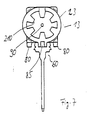
- FIG. 7 is the front view of another alternative versions 13 shown up to the size the cross-sectional area of the cap 20 of FIG. 1 Version 10 shown corresponds.
- the inner surface of the Cap 23 has inwardly projecting projections or webs 210 on, which reduce the receiving area of the cap 23.
- the Crosspieces 210 are formed in one piece with the cap 23 or in the form of a separate insert in the cap 23 can be used and locked with this.
- each version can also several, with respect to the direction of insertion of the photodiode 30 have successively arranged passages 50 into which a contact pin 60 can be used in each case. According to the selected number of contact pins it is possible to to control the mounted photodiode separately. Conveniently each socket can be made in one piece from an insulated Injection molding material can be produced.
- a connecting wire 70 is placed on each of the two supporting ends of the photodiode 30 each have a socket 10 postponed.
- the lead wire 70 is through the funnel-shaped inner surface of the cap 20 in the Holes 90 and 110 threaded and aligned by them and held. It is also assumed that the photodiode 30 at a predetermined location on one not shown circuit board to be connected. To for this purpose, the two sockets 10 have a precise distance from each other that the Corresponds to connection areas on the circuit board.
- the Cap 20 of the socket 10 is dimensioned such that not only an axial one, but advantageously one three-dimensional positioning is now possible the defined position of the photodiode 30 in relation to the two Versions 10 set. Then one each Contact pin 60 in the passage 50 of each socket 10 inserted until a press connection with the connecting wire 70 is made. So that the exact position of the Photodiode 30 not with respect to the sockets applied is lost, is via the inlet opening 180 advantageously a permanently elastic adhesive casting compound in introduced each cap 20. Can also be used as filler a UV-curable synthetic resin can be used.
- the Permanently elastic adhesive ensures that vibrations and external vibrations, for example in a Occur dampened on the electric or motor vehicle electronic component are transmitted. In this way can reliability in terms of contact-forming Press connection and the service life of the photodiode clearly be extended.
Landscapes
- Engineering & Computer Science (AREA)
- Microelectronics & Electronic Packaging (AREA)
- Power Engineering (AREA)
- Manufacturing & Machinery (AREA)
- Testing Of Individual Semiconductor Devices (AREA)
- Connector Housings Or Holding Contact Members (AREA)
- Measuring Fluid Pressure (AREA)
- Structures For Mounting Electric Components On Printed Circuit Boards (AREA)
- Coupling Device And Connection With Printed Circuit (AREA)
- Multi-Conductor Connections (AREA)
Description
- Fig. 1
- eine perspektivische Ansicht einer an einem Ende einer Fotodiode montierten erfindungsgemäßen Fassung,
- Fig. 2
- einen Längsschnitt der Fassung nach Fig. 1 entlang der Linie A-A,
- Fig. 3
- einen Querschnitt der Fassung nach Fig. 1 entlang der Linie B-B mit einem teilweise eingesetzten Kontaktstift,
- Fig. 4
- eine Vorderansicht einer Fassung mit zwei Kappen
- Fig. 5
- die Vorderansicht einer alternativen Fassung mit einer einzigen Kappe und zwei zugeordneten Kontaktelementen.
- Fig. 6
- die Draufsicht einer lösbaren Anordnung von vier Fassungen in Sternform,
- Fig. 7
- die Vorderansicht einer alternativen Fassung mit einer Kappe, deren Aufnahmebereich mittels Rippen verkleinert worden ist.
Claims (18)
- Fassung für elektrische und elektronische Komponenten mit Ausnahme von Leuchtmitteln,
mit folgenden Merkmalen:die Fassung (10, 11, 12, 13) ist einstückig ausgebildet und weist eine oder mehrere Kappen (20-23) mit einem einseitig geöffneten aufnahmebereich zur Aufnahme wenigstens eines vorbestimmten, wenigstens einen Anschlußkontakt (70) aufweisenden Teils einer elektrischen oder elektronischen Komponente (30), und ein Kontaktelement (60) auf,wobei die Kappe (20-23) derart bemessen ist, daß Fertigungsungenauigkeiten der Komponente (30) kompensierbar sind;jeder Kappe (20-23) ist wenigstens eine Kammer (50) zur Aufnahme des Kontaktelementes (60) zugeordnet, wobei das Kontaktelement (60) derart ausgebildet ist, daß es im eingesetzten Zustand mit dem Anschlußkontakt (70) innerhalb der Kammer (50) eine elektrisch leitende Preßverbindung bildet. - Fassung nach Anspruch 1, dadurch gekennzeichnet, daß die Querschnittsfläche des Aufnahmeraums der Kappe (20-23) sich in Einsetzrichtung der Komponente (30) verjüngt und daß ein erstes Loch (90) von der Kappe (20-23) in die Kammer (50) zum Einfädeln des Anschlußkontaktes (70) führt.
- Fassung nach Anspruch 1 oder 2, dadurch gekennzeichnet, daß die Kammer (50) in Bezug auf die Einsetzrichtung der Komponente (30) rechtwinklig verläuft und hinter der Kappe (20-23) angeordnet ist.
- Fassung nach einem der Ansprüche 2 oder 3, dadurch gekennzeichnet, daß die die Kammer (50) begrenzende Rückseite (100) der Fassung (10-13) ein zum ersten.Loch (90) fluchtendes zweites Loch (110) aufweist, wobei der Abstand zwischen den Löchern (90, 110) derart bemessen ist, daß die während des Einsetzens des Kontaktelements (60) auftretenden Kräfte im wesentlichen nicht in die Komponente (30) geleitet werden.
- Fassung nach einem der Ansprüche 1 bis 4, dadurch gekennzeichnet, daß die elektrische oder elektronische Komponente (30) mittels eines Füllmaterials, das durch eine Öffnung (180, 185) in die Kappe (20-23) einbringbar ist, fixierbar ist.
- Fassung nach Anspruch 5, dadurch gekennzeichnet, daß das Füllmaterial eine dauerelastische Klebevergußmasse ist.
- Fassung nach einem der Ansprüche 1 bis 6, gekennzeichnet durch Halte-, Rast- und/oder Führungseinrichtungen (190, 200) zum lösbaren Verbinden der Fassung (10, 11, 12, 13) mit wenigstens einer weiteren Fassung.
- Fassung nach einem der Ansprüche 1 bis 7, dadurch gekennzeichnet, daß der Fassung (11) mehrere in definierter Lage zueinander angeordnete Kappen (21) aufweist und daß jeder Kappe (21) eine Kammer zum Einsetzen eines Kontaktelements (60) zugeordnet ist.
- Fassung nach einem der Ansprüche 1 bis 8, dadurch gekennzeichnet, daß die Fassung (10-13) aus einem Dielektrikum hergestellt ist.
- Fassung nach einem der Ansprüche 1 bis 9, gekennzeichnet durch Positioniereinrichtungen (80) und/oder eine Führungsnut (85) zum gezielten Anordnen der Fassung (10, 11, 12, 13) an einem Träger.
- Fassung nach einem der Ansprüche 1 bis 10, dadurch gekennzeichnet, daß die Kappe (20-23) eine im wesentlichen ovale Querschnittsfläche hat.
- Fassung nach einem der Ansprüche 1 bis 11, dadurch gekennzeichnet, daß das Kontaktelement (60) ein Kontaktstift mit zwei Kontaktschenkeln (130, 135) ist, die im eingesetzten Zustand mit dem Anschlußkontakt (70) eine Preßverbindung bilden.
- Fassung nach Anspruch 12, dadurch gekennzeichnet, daß zwei Führungsnuten (120) in einem vorbestimmten Bereich der Kammer verlaufen und daß jeder Kontaktschenkel (130, 135) wenigstens einen Vorsprung (140, 145) aufweist, der beim Einsetzen des Kontaktelements (60) von der jeweiligen Führungsnut (120) aufgenommen wird.
- Fassung nach einem der Ansprüche 1 bis 13, dadurch gekennzeichnet, daß das Kontaktelement (60) Rasteinrichtungen (150) aufweist, die im eingesetzen Zustand das Kontaktelement (60) in der Kammer (50) fixieren.
- Fassung nach einem der Ansprüche 1 bis 14, dadurch gekennzeichnet, daß mehrere Kammern in bezug auf die Einsetzrichtung der Komponente hintereinander angeordnet sind.
- Fassung nach einem der Ansprüche 1 bis 15, dadurch gekennzeichnet, daß an der Innenfläche der Kappe (23) mehrere parallel zur Einsetzrichtung der Komponente verlaufende Rippen (210) angeordnet sind.
- Anordnung aus mehreren Fassungen nach einem der Ansprüche 1 bis 16, dadurch gekennzeichnet, daß die Fassungen lösbar oder fest miteinander verbunden sind.
- Verfahren zum Fixieren und Kontaktieren wenigstens einer elektrischen oder elektronischen Komponente innerhalb einer Fassung (10, 11, 12, 13) nach einem der Ansprüche 1 bis 15, mit folgenden Schritten:Einführen wenigstens eines vorbestimmten, wenigstens einen Anschlußkontakt aufweisenden Abschnitts der Komponente in die dem jeweiligen Abschnitt zugeordnete Kappe mit Freiraum zwischen der Kappe und dem Abschnitt,Festlegen einer definierten Lage der Komponente in Bezug auf jede Fassung,Einsetzen wenigstens eines Kontaktelementes in jede Kammer, die jeder Kappe zugeordnet ist, bis innerhalb der Kammer eine Preßverbindung mit dem Anschlußkontakt hergestellt ist,Fixieren der Komponente in Bezug auf jede Fassung durch Einfüllen eines Füllmaterials.
Applications Claiming Priority (2)
| Application Number | Priority Date | Filing Date | Title |
|---|---|---|---|
| DE19646523A DE19646523C2 (de) | 1996-11-12 | 1996-11-12 | Sockel für elektrische oder elektronische Komponenten |
| DE19646523 | 1996-11-12 |
Publications (3)
| Publication Number | Publication Date |
|---|---|
| EP0841728A2 EP0841728A2 (de) | 1998-05-13 |
| EP0841728A3 EP0841728A3 (de) | 1999-02-17 |
| EP0841728B1 true EP0841728B1 (de) | 2001-08-08 |
Family
ID=7811298
Family Applications (1)
| Application Number | Title | Priority Date | Filing Date |
|---|---|---|---|
| EP97119037A Expired - Lifetime EP0841728B1 (de) | 1996-11-12 | 1997-10-31 | Fassung für elektrische und elektronische Komponenten |
Country Status (3)
| Country | Link |
|---|---|
| EP (1) | EP0841728B1 (de) |
| DE (2) | DE19646523C2 (de) |
| ES (1) | ES2159080T3 (de) |
Families Citing this family (2)
| Publication number | Priority date | Publication date | Assignee | Title |
|---|---|---|---|---|
| DE19913660C2 (de) * | 1999-03-25 | 2001-08-30 | Bosch Gmbh Robert | Verfahren und Vorrichtung zur Befestigung elektrischer Bauelemente |
| FR3022701B1 (fr) * | 2014-06-24 | 2017-08-11 | Hypertac Sa | Module isolant destine a recevoir un contact electrique, ensemble de modules analogues, et connecteur comprenant au moins deux ensembles |
Family Cites Families (9)
| Publication number | Priority date | Publication date | Assignee | Title |
|---|---|---|---|---|
| DE2234726A1 (de) * | 1972-07-14 | 1974-01-24 | Siemens Ag | Bechergehaeuse zum isolations- und feuchteschutz sowie zur schirmung fuer ein elektrisches bauelement |
| DE2310151C3 (de) * | 1973-03-01 | 1975-10-23 | Rafi Raimund Finsterhoelzl Elektrotechnische Spezialfabrik, 7980 Ravensburg | Fassung für sockellose elektrische Kleinlampen |
| BR7602881A (pt) * | 1975-05-14 | 1977-05-10 | Itt | Conjunto conector eletrico que utiliza contatos livres |
| DE3146515A1 (de) * | 1981-11-24 | 1983-06-01 | Siemens AG, 1000 Berlin und 8000 München | Elektrisches bauelement mit radial angeordneten, zueinander parallelen stromzufuehrungsdraehten, das in einem kunststoffblock formvergossen eingeschlossen ist, und verfahren zu seiner herstellung |
| US4799896A (en) * | 1987-10-26 | 1989-01-24 | Edwin Gaynor Co. | Socket for compact fluorescent lamps |
| US5055071A (en) * | 1988-07-08 | 1991-10-08 | Carlson Russell L | In-line fuse holder |
| US5118308A (en) * | 1991-08-07 | 1992-06-02 | Pan-International Industrial Cop. | Bus connector |
| IT230348Y1 (it) * | 1993-07-12 | 1999-06-02 | Gallone Cesare | Dispositivo di supporto ed alimentazione per componenti elettrici |
| DE19520416C2 (de) * | 1995-06-02 | 1997-04-03 | Siemens Ag | Steckfassung |
-
1996
- 1996-11-12 DE DE19646523A patent/DE19646523C2/de not_active Expired - Fee Related
-
1997
- 1997-10-31 ES ES97119037T patent/ES2159080T3/es not_active Expired - Lifetime
- 1997-10-31 DE DE59704233T patent/DE59704233D1/de not_active Expired - Fee Related
- 1997-10-31 EP EP97119037A patent/EP0841728B1/de not_active Expired - Lifetime
Also Published As
| Publication number | Publication date |
|---|---|
| ES2159080T3 (es) | 2001-09-16 |
| DE59704233D1 (de) | 2001-09-13 |
| EP0841728A2 (de) | 1998-05-13 |
| DE19646523C2 (de) | 1999-06-02 |
| EP0841728A3 (de) | 1999-02-17 |
| DE19646523A1 (de) | 1998-05-14 |
Similar Documents
| Publication | Publication Date | Title |
|---|---|---|
| EP2672576B1 (de) | Steckverbinder für die Datenübertragung über elektrische Leiter | |
| DE29915553U1 (de) | Steckverbinder | |
| DE69416079T2 (de) | Klemmverbinder | |
| DE2536135A1 (de) | Elektrische verbindungsanordnung | |
| EP1155475A1 (de) | Elektrischer steckverbinder | |
| EP1467441A2 (de) | Schnellanschliessbare Steckverbindung in Spannzangentechnik | |
| DE2406417A1 (de) | Elektrischer verbinder zur verbindung eines koaxialkabels mit einer gedruckten schaltungsplatte | |
| DE69705115T2 (de) | Steckverbinder mit hoher dichte der anschlüsse | |
| DE4222685C2 (de) | Steckkontaktelement | |
| EP0483532A2 (de) | Leiterplattenklemmenanordnung | |
| DE29610415U1 (de) | Elektrischer Verbinder | |
| DE19646523C2 (de) | Sockel für elektrische oder elektronische Komponenten | |
| DE10323616A1 (de) | Schnellanschließbare Steckverbindung in Spannzangentechnik | |
| EP1632009B1 (de) | Kontaktelement und komplementäre leitungskammer für einen stecker oder eine buchse in schneidklemmtechnik | |
| DE20202835U1 (de) | Optische Verbindungseinrichtung | |
| EP0841729B1 (de) | Leuchtmittelfassung | |
| DE3531072C2 (de) | ||
| EP0905818A2 (de) | HF-Steckverbindungssystem und Verfahren zur Montage des HF-Steckverbindungssystems | |
| EP1286422B1 (de) | Baugruppe bestehend aus Schneidklemmkontakten und Aufpresshülsen | |
| DE3538485C1 (de) | Vorrichtung zum Fixieren stab- oder stiftfoermiger Elemente | |
| DE102023129565B4 (de) | Leiterplattenadapter zur kompakten und direkten elektrischen Kontaktierung von Leitern mit einer Leiterplatte | |
| DE3621483C2 (de) | ||
| DE9405555U1 (de) | Bauelement und Vorrichtung zu seiner Herstellung | |
| DE3920367A1 (de) | Vorrichtung zum verbinden einer vielzahl von draehten mit elektrischen kontakten | |
| DE10228307B4 (de) | Stiftleiste für eine Kontaktierung durch Schneidklemmen |
Legal Events
| Date | Code | Title | Description |
|---|---|---|---|
| PUAI | Public reference made under article 153(3) epc to a published international application that has entered the european phase |
Free format text: ORIGINAL CODE: 0009012 |
|
| AK | Designated contracting states |
Kind code of ref document: A2 Designated state(s): DE ES FR GB IT |
|
| PUAL | Search report despatched |
Free format text: ORIGINAL CODE: 0009013 |
|
| AK | Designated contracting states |
Kind code of ref document: A3 Designated state(s): AT BE CH DE DK ES FI FR GB GR IE IT LI LU MC NL PT SE |
|
| RHK1 | Main classification (correction) |
Ipc: H01R 33/02 |
|
| 17P | Request for examination filed |
Effective date: 19990811 |
|
| 17Q | First examination report despatched |
Effective date: 19990903 |
|
| AKX | Designation fees paid |
Free format text: DE ES FR GB IT |
|
| GRAG | Despatch of communication of intention to grant |
Free format text: ORIGINAL CODE: EPIDOS AGRA |
|
| RTI1 | Title (correction) |
Free format text: SOCKET FOR ELECTRICAL AND ELECTRONICAL COMPONENTS |
|
| GRAG | Despatch of communication of intention to grant |
Free format text: ORIGINAL CODE: EPIDOS AGRA |
|
| GRAH | Despatch of communication of intention to grant a patent |
Free format text: ORIGINAL CODE: EPIDOS IGRA |
|
| ITF | It: translation for a ep patent filed | ||
| GRAH | Despatch of communication of intention to grant a patent |
Free format text: ORIGINAL CODE: EPIDOS IGRA |
|
| GRAA | (expected) grant |
Free format text: ORIGINAL CODE: 0009210 |
|
| AK | Designated contracting states |
Kind code of ref document: B1 Designated state(s): DE ES FR GB IT |
|
| GBT | Gb: translation of ep patent filed (gb section 77(6)(a)/1977) |
Effective date: 20010808 |
|
| REF | Corresponds to: |
Ref document number: 59704233 Country of ref document: DE Date of ref document: 20010913 |
|
| REG | Reference to a national code |
Ref country code: ES Ref legal event code: FG2A Ref document number: 2159080 Country of ref document: ES Kind code of ref document: T3 |
|
| ET | Fr: translation filed | ||
| PG25 | Lapsed in a contracting state [announced via postgrant information from national office to epo] |
Ref country code: ES Free format text: LAPSE BECAUSE OF NON-PAYMENT OF DUE FEES Effective date: 20011101 |
|
| PG25 | Lapsed in a contracting state [announced via postgrant information from national office to epo] |
Ref country code: GB Free format text: LAPSE BECAUSE OF NON-PAYMENT OF DUE FEES Effective date: 20011108 |
|
| REG | Reference to a national code |
Ref country code: GB Ref legal event code: IF02 |
|
| PLBE | No opposition filed within time limit |
Free format text: ORIGINAL CODE: 0009261 |
|
| STAA | Information on the status of an ep patent application or granted ep patent |
Free format text: STATUS: NO OPPOSITION FILED WITHIN TIME LIMIT |
|
| GBPC | Gb: european patent ceased through non-payment of renewal fee |
Effective date: 20011108 |
|
| PG25 | Lapsed in a contracting state [announced via postgrant information from national office to epo] |
Ref country code: DE Free format text: LAPSE BECAUSE OF NON-PAYMENT OF DUE FEES Effective date: 20020702 |
|
| 26N | No opposition filed | ||
| PGFP | Annual fee paid to national office [announced via postgrant information from national office to epo] |
Ref country code: FR Payment date: 20031003 Year of fee payment: 7 |
|
| REG | Reference to a national code |
Ref country code: ES Ref legal event code: FD2A Effective date: 20021113 |
|
| PG25 | Lapsed in a contracting state [announced via postgrant information from national office to epo] |
Ref country code: FR Free format text: LAPSE BECAUSE OF NON-PAYMENT OF DUE FEES Effective date: 20050630 |
|
| REG | Reference to a national code |
Ref country code: FR Ref legal event code: ST |
|
| PG25 | Lapsed in a contracting state [announced via postgrant information from national office to epo] |
Ref country code: IT Free format text: LAPSE BECAUSE OF NON-PAYMENT OF DUE FEES Effective date: 20051031 |