EP0840456A2 - PLL frequency synthesizer capable of changing an output frequency at a high speed - Google Patents
PLL frequency synthesizer capable of changing an output frequency at a high speed Download PDFInfo
- Publication number
- EP0840456A2 EP0840456A2 EP97204137A EP97204137A EP0840456A2 EP 0840456 A2 EP0840456 A2 EP 0840456A2 EP 97204137 A EP97204137 A EP 97204137A EP 97204137 A EP97204137 A EP 97204137A EP 0840456 A2 EP0840456 A2 EP 0840456A2
- Authority
- EP
- European Patent Office
- Prior art keywords
- signal
- frequency
- phase
- pulse
- supplied
- Prior art date
- Legal status (The legal status is an assumption and is not a legal conclusion. Google has not performed a legal analysis and makes no representation as to the accuracy of the status listed.)
- Withdrawn
Links
- 239000003990 capacitor Substances 0.000 claims abstract description 16
- 230000007423 decrease Effects 0.000 claims description 7
- 238000001914 filtration Methods 0.000 claims description 6
- 238000001208 nuclear magnetic resonance pulse sequence Methods 0.000 claims description 4
- 238000005070 sampling Methods 0.000 claims description 2
- 238000010586 diagram Methods 0.000 description 10
- 230000001052 transient effect Effects 0.000 description 4
- 230000003247 decreasing effect Effects 0.000 description 2
- 230000002950 deficient Effects 0.000 description 2
- 230000003111 delayed effect Effects 0.000 description 1
- 230000005669 field effect Effects 0.000 description 1
- 239000004065 semiconductor Substances 0.000 description 1
Images


Classifications
-
- H—ELECTRICITY
- H03—ELECTRONIC CIRCUITRY
- H03L—AUTOMATIC CONTROL, STARTING, SYNCHRONISATION OR STABILISATION OF GENERATORS OF ELECTRONIC OSCILLATIONS OR PULSES
- H03L7/00—Automatic control of frequency or phase; Synchronisation
- H03L7/06—Automatic control of frequency or phase; Synchronisation using a reference signal applied to a frequency- or phase-locked loop
- H03L7/16—Indirect frequency synthesis, i.e. generating a desired one of a number of predetermined frequencies using a frequency- or phase-locked loop
- H03L7/18—Indirect frequency synthesis, i.e. generating a desired one of a number of predetermined frequencies using a frequency- or phase-locked loop using a frequency divider or counter in the loop
- H03L7/183—Indirect frequency synthesis, i.e. generating a desired one of a number of predetermined frequencies using a frequency- or phase-locked loop using a frequency divider or counter in the loop a time difference being used for locking the loop, the counter counting between fixed numbers or the frequency divider dividing by a fixed number
-
- H—ELECTRICITY
- H03—ELECTRONIC CIRCUITRY
- H03L—AUTOMATIC CONTROL, STARTING, SYNCHRONISATION OR STABILISATION OF GENERATORS OF ELECTRONIC OSCILLATIONS OR PULSES
- H03L7/00—Automatic control of frequency or phase; Synchronisation
- H03L7/06—Automatic control of frequency or phase; Synchronisation using a reference signal applied to a frequency- or phase-locked loop
- H03L7/08—Details of the phase-locked loop
- H03L7/085—Details of the phase-locked loop concerning mainly the frequency- or phase-detection arrangement including the filtering or amplification of its output signal
- H03L7/089—Details of the phase-locked loop concerning mainly the frequency- or phase-detection arrangement including the filtering or amplification of its output signal the phase or frequency detector generating up-down pulses
- H03L7/0891—Details of the phase-locked loop concerning mainly the frequency- or phase-detection arrangement including the filtering or amplification of its output signal the phase or frequency detector generating up-down pulses the up-down pulses controlling source and sink current generators, e.g. a charge pump
- H03L7/0895—Details of the current generators
- H03L7/0898—Details of the current generators the source or sink current values being variable
-
- H—ELECTRICITY
- H03—ELECTRONIC CIRCUITRY
- H03L—AUTOMATIC CONTROL, STARTING, SYNCHRONISATION OR STABILISATION OF GENERATORS OF ELECTRONIC OSCILLATIONS OR PULSES
- H03L7/00—Automatic control of frequency or phase; Synchronisation
- H03L7/06—Automatic control of frequency or phase; Synchronisation using a reference signal applied to a frequency- or phase-locked loop
- H03L7/08—Details of the phase-locked loop
- H03L7/10—Details of the phase-locked loop for assuring initial synchronisation or for broadening the capture range
- H03L7/107—Details of the phase-locked loop for assuring initial synchronisation or for broadening the capture range using a variable transfer function for the loop, e.g. low pass filter having a variable bandwidth
- H03L7/1072—Details of the phase-locked loop for assuring initial synchronisation or for broadening the capture range using a variable transfer function for the loop, e.g. low pass filter having a variable bandwidth by changing characteristics of the charge pump, e.g. changing the gain
-
- H—ELECTRICITY
- H03—ELECTRONIC CIRCUITRY
- H03L—AUTOMATIC CONTROL, STARTING, SYNCHRONISATION OR STABILISATION OF GENERATORS OF ELECTRONIC OSCILLATIONS OR PULSES
- H03L7/00—Automatic control of frequency or phase; Synchronisation
- H03L7/06—Automatic control of frequency or phase; Synchronisation using a reference signal applied to a frequency- or phase-locked loop
- H03L7/08—Details of the phase-locked loop
- H03L7/14—Details of the phase-locked loop for assuring constant frequency when supply or correction voltages fail or are interrupted
- H03L7/146—Details of the phase-locked loop for assuring constant frequency when supply or correction voltages fail or are interrupted by using digital means for generating the oscillator control signal
-
- H—ELECTRICITY
- H03—ELECTRONIC CIRCUITRY
- H03L—AUTOMATIC CONTROL, STARTING, SYNCHRONISATION OR STABILISATION OF GENERATORS OF ELECTRONIC OSCILLATIONS OR PULSES
- H03L7/00—Automatic control of frequency or phase; Synchronisation
- H03L7/06—Automatic control of frequency or phase; Synchronisation using a reference signal applied to a frequency- or phase-locked loop
- H03L7/16—Indirect frequency synthesis, i.e. generating a desired one of a number of predetermined frequencies using a frequency- or phase-locked loop
- H03L7/18—Indirect frequency synthesis, i.e. generating a desired one of a number of predetermined frequencies using a frequency- or phase-locked loop using a frequency divider or counter in the loop
- H03L7/183—Indirect frequency synthesis, i.e. generating a desired one of a number of predetermined frequencies using a frequency- or phase-locked loop using a frequency divider or counter in the loop a time difference being used for locking the loop, the counter counting between fixed numbers or the frequency divider dividing by a fixed number
- H03L7/187—Indirect frequency synthesis, i.e. generating a desired one of a number of predetermined frequencies using a frequency- or phase-locked loop using a frequency divider or counter in the loop a time difference being used for locking the loop, the counter counting between fixed numbers or the frequency divider dividing by a fixed number using means for coarse tuning the voltage controlled oscillator of the loop
- H03L7/189—Indirect frequency synthesis, i.e. generating a desired one of a number of predetermined frequencies using a frequency- or phase-locked loop using a frequency divider or counter in the loop a time difference being used for locking the loop, the counter counting between fixed numbers or the frequency divider dividing by a fixed number using means for coarse tuning the voltage controlled oscillator of the loop comprising a D/A converter for generating a coarse tuning voltage
-
- H—ELECTRICITY
- H03—ELECTRONIC CIRCUITRY
- H03L—AUTOMATIC CONTROL, STARTING, SYNCHRONISATION OR STABILISATION OF GENERATORS OF ELECTRONIC OSCILLATIONS OR PULSES
- H03L7/00—Automatic control of frequency or phase; Synchronisation
- H03L7/06—Automatic control of frequency or phase; Synchronisation using a reference signal applied to a frequency- or phase-locked loop
- H03L7/16—Indirect frequency synthesis, i.e. generating a desired one of a number of predetermined frequencies using a frequency- or phase-locked loop
- H03L7/18—Indirect frequency synthesis, i.e. generating a desired one of a number of predetermined frequencies using a frequency- or phase-locked loop using a frequency divider or counter in the loop
- H03L7/197—Indirect frequency synthesis, i.e. generating a desired one of a number of predetermined frequencies using a frequency- or phase-locked loop using a frequency divider or counter in the loop a time difference being used for locking the loop, the counter counting between numbers which are variable in time or the frequency divider dividing by a factor variable in time, e.g. for obtaining fractional frequency division
- H03L7/1972—Indirect frequency synthesis, i.e. generating a desired one of a number of predetermined frequencies using a frequency- or phase-locked loop using a frequency divider or counter in the loop a time difference being used for locking the loop, the counter counting between numbers which are variable in time or the frequency divider dividing by a factor variable in time, e.g. for obtaining fractional frequency division for reducing the locking time interval
Definitions
- This invention relates to a frequency synthesizer with a phase-locked loop (PLL).
- PLL phase-locked loop
- the PLL frequency synthesizer comprises a reference signal generator, a voltage controlled oscillator, a variable frequency divider, a phase-frequency comparator, and a control voltage supplying circuit.
- the reference signal generator generates a reference signal with a reference frequency. Responsive to a control voltage signal, the voltage controlled oscillator generates a voltage controlled signal having a controllable oscillating frequency.
- the PLL frequency synthesizer produces the voltage controlled signal as an output signal. Therefore, the output signal has an output frequency equal to the controllable oscillating frequency.
- the output signal is supplied to the variable frequency divider.
- the variable frequency divider is also supplied with a designated dividing number D which defines the output frequency, where D represents a positive integer.
- the variable frequency divider frequency divides the output signal on the basis of the designated dividing number D to produce a divided signal.
- the variable frequency divider is for frequency dividing the output signal by a factor l/D.
- the phase-frequency comparator is supplied with the reference signal and the divided signal.
- the phase-frequency comparator detects a phase-frequency difference between the reference signal and the divided signal to produce a phase-frequency difference signal indicative of the phase-frequency difference.
- the phase-frequency difference signal indicates one of lag and lead phases which the divided signal has in comparison with the reference signal.
- the control voltage supplying circuit supplies the control voltage signal to the voltage controlled oscillator.
- the control voltage supplying circuit comprises a current flow control circuit and a loop filter. Responsive to the phase-frequency difference signal, the current flow control circuit controls flow-in and flow-out of current supplied therefrom/to to produce a current flow control signal.
- the current flow control signal indicates the flow-out of the current when the phase-frequency difference signal indicates the lag phase.
- the current flow control signal indicates the flow-in of the current when the phase-frequency difference signal indicates the lead phase.
- the loop filter filters the current flow control signal into a filtered signal as the control voltage signal. More particularly, the loop filter comprises a filter capacitor which is selectively charged and discharged when the current flow control signal indicates the flow-out and the flow-in of the current, respectively.
- a conventional PLL frequency synthesizer changing of the output frequency is carried out by changing step by step the designated dividing number D. Therefore, the PLL frequency synthesizer has a variable delay amount on changing the output frequency. As a result, a frequency error of the output frequency occurs in the PLL frequency synthesizer on changing the output frequency. Accordingly, the conventional PLL frequency synthesizer is defective in that it is impossible to change the output frequency at a high speed.
- a frequency synthesizer comprises a reference signal generator for generating a reference signal with a reference frequency, a voltage controlled oscillator responsive to a control voltage signal for generating an output signal having an output frequency, a variable frequency divider supplied with the output signal and responsive to a designated dividing number defining the output frequency for frequency dividing the output signal on the basis of the designated dividing number to produce a divided signal, a first pulse removing circuit supplied with the reference signal and responsive to first removing data indicative of a first pulse number for removing pulses from the reference signal that are equal in number to the first pulse number for a first predetermined cycle to produce a first pulse removed signal, a second pulse removing circuit supplied with the divided signal and responsive to second removing data indicative of a second pulse number for removing pulses from the divided signal that are equal in number to the second pulse number for a second predetermined cycle to produce a second pulse removed signal, a phase-frequency comparator supplied with the first and the second pulse removed signals for detecting a phase-
- a frequency synthesizer comprises a reference signal generator for generating a reference signal with a reference frequency, a voltage controlled oscillator responsive to a control voltage signal for generating an output signal having an output frequency, a variable frequency divider supplied with the output signal and responsive to a designated dividing number defining the output frequency for frequency dividing the output signal on the basis of the designated dividing number to produce a divided signal, a phase-frequency comparator supplied with the reference signal and the divided signal for detecting a phase-frequency difference between the reference signal and the divided signal to produce a phase-frequency difference signal indicating one of lag and lead phases which the divided signal has in comparison with the reference signal, a current flow control circuit responsive to the phase-frequency difference signal for controlling flow-in and flow-out of current supplied therefrom/to to produce a current flow control signal, a loop filter supplied with the current flow control signal for filtering the current flow control signal into a filtered signal as the control voltage signal, and a current controlling circuit responsive to a current command for
- a frequency synthesizer comprises a reference signal generator for generating a reference signal with a reference frequency, a voltage controlled oscillator responsive to a control voltage signal for generating an output signal having an output frequency, a variable frequency divider supplied with the output signal and responsive to a designated dividing number defining the output frequency for frequency dividing the output signal on the basis of the designated dividing number to produce a divided signal, a phase-frequency comparator supplied with the reference signal and the divided signal for detecting a phase-frequency difference between the reference signal and the divided signal to produce a phase-frequency difference signal indicating one of lag and lead phases which the divided signal has in comparison with the reference signal, a current flow control circuit responsive to the phase-frequency difference signal for controlling flow-in and flow-out of current supplied therefrom/to to produce a current flow control signal, and a loop filter supplied with the current flow control signal for filtering the current flow control signal into a filtered signal as the control voltage signal.
- the above-mentioned current flow control circuit comprises a control circuit responsive to the phase-frequency difference signal for producing first through third control signals, a constant current circuit responsive to the first control signal for producing a constant current, an integrating circuit having an initial voltage for integrating the constant current to an integrated voltage, the integrating circuit being reset from the integrated voltage to the initial voltage in response to the second control signal, and a sample and hold circuit responsive to the third control signal for sampling the integrated voltage to hold a sampled voltage as a held signal, the sample and hold circuit producing the held signal as the current flow control signal.
- a frequency synthesizer comprises a reference signal generator for generating a reference signal with a reference frequency, a voltage controlled oscillator responsive to a control voltage signal for generating an output signal having an output frequency, a variable frequency divider supplied with the output signal and responsive to a designated dividing number defining the output frequency for frequency dividing the output signal on the basis of the designated dividing number to produce a divided signal, a phase-frequency comparator supplied with the reference signal and the divided signal for detecting a phase-frequency difference between the reference signal and the divided signal to produce a phase-frequency difference signal indicative of the phase-frequency difference, modifying means connected to the phase-frequency comparator and responsive to a control enable signal for modifying the phase-frequency difference signal into a modified signal, and a control voltage supplying circuit supplied with the modified signal for supplying the control voltage signal to the voltage controlled oscillator in response to the modified signal.
- a frequency synthesizer comprises a reference signal generator for generating a reference signal with a reference frequency, a voltage controlled oscillator responsive to a control voltage signal for generating an output signal having an output frequency, a variable frequency divider supplied with the output signal and responsive to a designated dividing number defining the output frequency for frequency dividing the output signal on the basis of the designated dividing number to produce a divided signal, a phase-frequency comparator supplied with the reference signal and the divided signal for detecting a phase-frequency difference between the reference signal and the divided signal to produce a phase-frequency difference signal indicative of the phase-frequency difference, a current flow control circuit responsive to the phase-frequency difference signal for controlling flow-in and flow-out of current therefrom/to to produce a current flow control signal, a loop filter supplied with the current flow control signal for filtering the current flow control signal into a filtered signal, the loop filter comprising a filter capacitor which is selectively charged and discharged in accordance with the current flow control signal, a control circuit supplied
- a conventional PLL frequency synthesizer will be described at first in order to facilitate an understanding of the present invention.
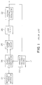
- the PLL frequency synthesizer comprises a reference signal generator 21, a voltage controlled oscillator 22, a variable frequency divider 23, a phase-frequency comparator 24, a charge pump circuit 25, and a loop filter 26.
- the reference signal generator 21 generates a reference signal with a reference frequency.
- the voltage controlled oscillator 22 is supplied with a control voltage signal in the manner which will become clear as the description proceeds. Responsive to the control voltage signal, the voltage controlled oscillator 22 generates a voltage controlled signal having a controllable oscillating frequency.
- the PLL frequency synthesizer produces the voltage controlled signal as an output signal. Therefore, the output signal has an output frequency equal to the controllable oscillating frequency.
- the output signal is supplied to the variable frequency divider 23.
- the variable frequency divider 23 is also supplied with a designated dividing number D which defines the output frequency, where D represents a positive integer.
- the variable frequency divider 23 frequency divides the output signal on the basis of the designated dividing number D to produce a divided signal.
- the variable frequency divider 23 is for frequency dividing the output signal by a factor l/D.
- the phase-frequency comparator 24 is supplied with the reference signal and the divided signal.
- the phase-frequency comparator 24 detects a phase-frequency difference between the reference signal and the divided signal to produce a phase-frequency difference signal indicative of the phase-frequency difference.
- the phase-frequency difference signal indicates one of lag and lead phases which the divided signal has in comparison with the reference signal.
- the phase-frequency difference signal is supplied with the charge pump circuit 25.
- the charge pump circuit 25 acts as a current flow control circuit which is for controlling flow-in and flow-out of current supplied therefrom/to to produce a current flow control signal.
- the current flow control signal indicates the flow-out of the current when the phase-frequency difference signal indicates the lag phase.
- the current flow control signal indicates the flow-in of the current when the phase-frequency difference signal indicates the lead phase.
- the current flow control signal is supplied with the loop filter 26.
- the loop filter filters the current flow control signal into a filtered signal as the control voltage signal. More particularly, the loop filter 26 comprises a filter capacitor (not shown) which is selectively charged and discharged when the current flow control signal indicates the flow-out and the flow-in of the current, respectively.
- a combination of the charge pump circuit 25 and the loop filter 26 serves as a control voltage supplying circuit for supplying the control voltage signal to the voltage controlled oscillator in response to the phase-frequency difference signal.
- the PLL frequency synthesizer produces the output signal having the output frequency which is equal to D times as large as the reference frequency of the reference signal. It is therefore possible to change the output frequency by changing the designated dividing number D.
- changing of the output frequency is carried out by changing step by step the designated dividing number D.
- the conventional PLL frequency synthesizer is defective in that it is impossible to change the output frequency at a high speed, as mentioned in the preamble of the instant specification.
- the PLL frequency synthesizer is similar in structure and operation to the conventional PLL frequency synthesizer illustrated in Fig. 1 except that the PLL frequency synthesizer further comprises first and second pulse removing circuits 31 and 32.
- the first pulse removing circuit 31 is connected between the reference signal generator 21 and the phase-frequency comparator 24.
- the second pulse removing circuit 32 is connected between the variable frequency divider 23 and the phase-frequency comparator 24.
- the first pulse removing circuit 31 is supplied with the reference signal from the reference signal generator 21 and first removing data A1 indicative of a first pulse number. Responsive to the first removing data A1, the first pulse removing circuit 31 removes pulses from the reference signal that are equal in number to the first pulse number for a first predetermined cycle to produce a first pulse removed signal. Instead of the reference signal, the first pulse removed signal is supplied to the phase-frequency comparator 24.
- the second pulse removing circuit 32 is supplied with the divided signal from the variable frequency divider 23 and second removing data A2 indicative of a second pulse number.
- the second pulse removing circuit 32 removes pulses from the divided signal that are equal in number to the second pulse number for a second predetermined cycle to produce a second pulse removed signal. Instead of the divided signal, the second pulse removed signal is supplied to the phase-frequency comparator 24.
- the phase-frequency comparator 24 detects a phase-frequency difference between the first and the second pulse removed signals to produce a phase-frequency difference signal indicative of the phase-frequency difference.
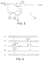
- the first pulse removing circuit 31 comprises a first inverter 311, a first counter 312, and a first AND gate 313.
- the first inverter 311 is supplied with the reference signal from the reference signal generator 21 (Fig. 2) as a first input pulse signal.
- the first inverter 311 inverts the first input pulse signal to produce a first inverted pulse signal.
- the first inverter 311 is connected to the first counter 312 which is supplied with the first pulse removing data.
- the first counter 312 counts up a first count in synchronism with the first inverted pulse signal.
- the first counter 312 produces a first time-up signal when the first count increases up to the first pulse number.
- the first time-up signal is supplied to the first AND gate 313 which is supplied with the first input pulse signal. Responsive to the first input pulse signal and the first time-up signal, the first AND gate 313 produces a first AND'ed signal as the first pulse removed signal.
- the second pulse removing circuit 32 comprises a second inverter 321, a second counter 322, and a second AND gate 323.
- the second inverter 321 is supplied with the divided signal from the variable frequency divider 23 (Fig. 2) as a second input pulse signal.
- the second inverter 321 inverts the second input pulse signal to produce a second inverted pulse signal.
- the second inverter 321 is connected to the second counter 322 which is supplied with the second pulse removing data.
- the second counter 322 counts up a second count in synchronism with the second inverted pulse signal.
- the second counter 322 produces a second time-up signal when the second count increases up to the second pulse number.
- the second time-up signal is supplied to the second AND gate 323 which is supplied with the second input pulse signal. Responsive to the second input pulse signal and the second time-up signal, the second AND gate 323 produces a second AND'ed signal as the second pulse removed signal.
- the first input pulse signal is depicted along Fig. 4(a).
- the first input pulse signal is inverted by the first inverter 311 into the first inverted pulse signal as shown in Fig. 4(b).
- the first inverter 311 has an inverting delay time denoted to d1.
- the first counter 312 is supplied with the first pulse removing data indicative of the first pulse number equal to four. In this event, the first counter 312 counts up the first count at a leading edge of each pulse in the first inverted pulse signal. The first counter 312 produces the first time-up signal of a logical "1" level when the first count increases up to the first pulse number, namely, four, as shown in Fig. 4(c). The first counter 312 is reset to produce the first time-up signal of a logical "0" level in response to another leading edge of the next succeeding pulse of the first inverted pulse signal. The first counter 312 has a counting delay time denoted to d2.
- the first AND gate 313 produces the first AND'ed signal as the first pulse removed signal as shown in Fig. 4(d). That is, the first AND gate 313 produces the first pulse removed signal having pulses which is one-fifth as large as those of the first input pulse signal. In other words, the first pulse removing circuit 31 removes four pulses from the reference signal for the first predetermined cycle which has five pulses.
- the first AND gate 313 has a gate delay time denoted to d3.
- the first counter 312 continuously produces the first time-up signal with the logical "1" level.
- the first AND gate 313 produces the first pulse removed signal to which the first input pulse signal is delayed for the gate delay time t3 by the first AND gate 313 as shown in Fig. 4(e).
- Operation of the second pulse removing circuit 32 is similar to that of the first pulse removing circuit 31 and the description thereof is therefore omitted.
- the PLL frequency synthesizer is similar in structure and operation to the conventional PLL frequency synthesizer illustrated in Fig. 1 except that the PLL frequency synthesizer further comprises a current controlling circuit 35.
- the current controlling circuit 35 is connected to the charge pump circuit 25 and is supplied with a current command C. Responsive to the current command C, the current controlling circuit 35 controls the current for the charge pump circuit 25. More specifically, the current command C is present while the output frequency is changed. The current controlling circuit 35 controls the current so as to increase the current when the current command C is present and then to gradually decrease the current after the current command C becomes absent. A little more in detail, the current controlling circuit 35 comprises a charge-up control circuit and a discharge control circuit.
- the charge pump circuit 25 comprises a complementary-symmetry metal-oxide-semiconductor field-effect transistor (CMOSFET) which consists of a p-channel MOSFET 36 and an n-channel MOSFET 37.
- CMOSFET complementary-symmetry metal-oxide-semiconductor field-effect transistor
- Each of the MOSFETs 36 and 37 has a gate terminal, a drain terminal, and a source terminal.
- the p-channel and the n-channel MOSFETs 36 and 37 are joined at their drain terminals which are connected to the loop filter 26 (Fig. 5).
- the p-channel MOSFET 36 has the source terminal which is connected to the charge-up control circuit of the current controlling circuit 35.
- the n-channel MOSFET 37 has the source terminal which is connected to the discharge control circuit of the current controlling circuit 35.
- Both of the p-channel and the n-channel MOSFETs 36 and 37 have the gate terminals which are connected to the phase-frequency comparator 24 (Fig. 5). More particularly, the phase-frequency difference signal comprises lag and lead phase signals which indicate the lag and the lead phases, respectively.
- the lag phase signal is supplied to the gate terminal of the p-channel MOSFET 36.
- the lead phase signal is supplied to the gate terminal of the n-channel MOSFET 37.
- the p-channel MOSFET 36 Supplied with the lag phase signal, the p-channel MOSFET 36 is put into an ON state, thereby the current flows from the charge-up control circuit to the loop filter 26 through the p-channel MOSFET 36.
- the n-channel MOSFET 37 Supplied with the lead phase signal, the n-channel MOSFET 37 is put into an ON state, thereby the current flows from the loop filter 26 to the discharge control circuit through the n-channel MOSFET 37.
- the charge-up control circuit of the current controlling circuit 36 comprises a switching element 41, an operational amplifier 42, an n-channel MOSFET 43, first and second p-channel MOSFETs 44 and 45, first through third resistors 46, 47, and 48, and a capacitor 49.
- the operational amplifier 42 has an inverting input terminal, a noninverting input terminal, and an amplifier output terminal.
- the switching element 41 has a control input terminal supplied with the current command C.
- the switching element 41 is supplied with a positive source voltage +V DD .
- the switching element 41 is connected to the noninverting input terminal of the operational amplifier 42.
- the switching element 41 turns on, thereby the positive source voltage +V DD is supplied to the noninverting input terminal of the operational amplifier 42.
- the inverting input terminal of the operational amplifier 42 is an end of the first resistor 46 which has another end grounded.
- the noninverting input terminal of the operational amplifier 42 is connected to an end of the second resistor 47 which has another end grounded.
- the second resistor 47 is connected to the capacitor 49 in parallel.
- the noninverting input terminal of the operational amplifier 42 is also connected to an end of the third resistor 47 which has another end supplied with the positive source voltage +V DD .
- the amplifier output terminal of the operational amplifier 42 is connected to the gate terminal of the n-channel MOSFET 43 which has the source terminal connected to the inverting input terminal of the operational amplifier 42.
- the n-channel MOSFET 43 has the drain terminal which is connected to the drain terminal of the first p-channel MOSFET 44.
- the drain terminal of the n-channel MOSFET 43 is also connected to the gate terminals of the first and the second p-channel MOSFETs 44 and 45.
- Both of the first and the second p-channel MOSFETs 44 and 45 have the source terminals which are supplied with the positive source voltage +V DD .
- the second p-channel MOSFET 45 has the drain terminal which is connected to the source terminal of the p-channel MOSFET 36 (Fig. 6). Therefore, a combination of the first and the second p-channel MOSFETs 44 and 45 composes a current Miller circuit.
- the second p-channel MOSFET 45 has a gate width which is N times as large as that of the first p-channel MOSFET 44, where N represents a predetermined number.
- N represents a predetermined number.
- Figs. 8(a) through (c) description will be made as regards operation of the charge-up control circuit of the current controlling circuit 36 illustrated in Fig. 7. It will be assumed that the first through the third resistors 46 to 48 have first through third resistance values, respectively, which are denoted to R 46 , R 47 , and R 48 . The third resistance value R 48 is larger than the second resistance value R 47 .
- Figs. 8(a) through (c) show the current command C, and the first and the second drain currents D 1 and D 2 , respectively.
- the switching element 41 turns on. Therefore, the capacitor 49 is charged up to a voltage of V DD .
- the n-channel MOSFET 43 flows the first drain current D 1 which has a current value of V DD /R 46 . Therefore, through the second p-channel MOSFET 45 flows the second drain current D 2 which has a current value of N x V DD /R 46 .
- the switching element 41 turns off. Therefore, the capacitor 49 is exponentially discharged up to a voltage of R 47 /(R 47 + R 48 )) x V DD .
- the first drain current D 1 exponentially decreases up to a current value of (R 47 /(R 47 + R 48 )) x V DD /R 46 .
- the second drain current D 2 exponentially decreases up to a current value of N x (R 47 /(R 47 + R 48 )) x V DD /R 46 .
- the discharge control circuit of the current controlling circuit 35 is similar in structure and operation to the charge-up control circuit illustrated in Fig. 7 except that the n-channel MOSFET 43 is replaced with a p-channel MOSFET, the p-channel MOSFETs 44 and 45 are replaced with n-channel MOSFETs, and the positive source voltage +V DD and the ground are exchanged each other.
- the PLL frequency synthesizer is similar in structure and operation to the conventional PLL frequency synthesizer illustrated in Fig. 1 except that the charge pump circuit is modified from that illustrated in Fig. 1 as will later become clear. The charge pump circuit is therefore depicted at 25a.
- the illustrated charge pump circuit 25a comprises a control circuit 51, a constant current circuit 52, an integrating circuit 53, and a sample and hold circuit 54.
- the control circuit 51 is connected to the phase-frequency comparator 24. Responsive to the phase-frequency difference signal, the control circuit 51 produces first through third control signals. The first through the third control signals are supplied to the constant current circuit 52, the integrating circuit 53, and the sample and hold circuit 54, respectively.
- the constant current circuit 52 produces a constant current.
- the constant current is supplied to the integrating circuit 53.
- the integrating circuit 53 has an initial voltage.
- the integrating circuit 53 integrates the constant current to an integrated voltage.
- the integrating circuit 53 is reset from the integrated voltage to the initial voltage in response to the second control signal.
- the integrated voltage is supplied to the sample and hold circuit 54.
- the sample and hold circuit 44 samples the integrated voltage to hold a sampled voltage as a held signal.
- the sample and hold circuit 44 supplies the held signal to the loop filter 26 as the current flow control signal.
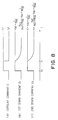
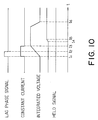
- Fig. 10 in addition to Fig. 9, description will be made as regards operation of the charge pump circuit 25a.
- Fig. 10 the lag phase signal, the constant current, the integrated voltage, and the held signal are depicted along first through fourth lines.
- the lag phase signal is supplied from the phase-frequency comparator 24 to the control circuit 51 during a first time duration between a first time instant t 1 and a second time instant t 2 .
- the control circuit 51 produces the first control signal during a second time duration between the first time instant t 1 and a third time instant t 3 .
- the constant current circuit 52 produces the constant current during the second time duration as shown in the second line in Fig. 10. Therefore, the integrating circuit 53 integrates the constant current to the integrated voltage during the second time duration as shown in the third line in Fig. 10. After the third time instant t 3 , the integrating circuit 53 keeps the integrated voltage.
- the control circuit 51 produces the third control signal. Responsive to the third control signal, the sample and hold circuit 44 samples the integrated voltage to hold a sampled voltage as a held signal at a fifth time instant t 5 . The held signal is supplied to the loop filter 26 as the current flow control signal. At a sixth time instant t 6 , the control circuit 51 produces the second control signal. Responsive to the second control signal, the integrating circuit 53 is reset from the integrated voltage to the initial voltage. Therefore, the charge pump circuit 25a increases a level of the current flow control signal in response to the lag phase signal. In the similar operation, the charge pump circuit 25a decreases the level of the current flow control signal in response to the lead phase signal.
- the PLL frequency synthesizer is similar in structure and operation to the conventional PLL frequency synthesizer illustrated in Fig. 1 except that the PLL frequency synthesizer further comprises a control circuit 60.
- the control circuit 60 is connected between the phase-frequency comparator 24 and the charge pump circuit 25.
- the control circuit 60 is supplied with a control enable signal CE. Responsive to the control enable signal CE, the control circuit 60 acts as a modifying arrangement for modifying the phase-frequency difference signal into a modified signal. Instead of the phase-frequency difference signal, the modified signal is supplied to the charge pump circuit 25. Therefore, the charge pump circuit 25 controls, in response to the modified signal, flow-in and flow-out of the current supplied therefrom/to to produce the current flow control signal.
- the control circuit 60 is operable in one of a first mode and a second mode. At first, the first mode will be described. The second mode will be described later in the following.
- the control enable signal CE is present while the output frequency is changed.
- the phase-frequency difference signal comprises a pulse sequence having pulses for a predetermined cycle that are equal in number to a controllable number.
- the control circuit 60 gradually decreases the controllable number until at last a predetermined final number.
- the predetermined final number is, for example, one sixty-fourths as large as the controllable number before being decreased.
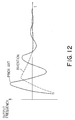
- Fig. 12 shows transient responses of the output frequency in the conventional PLL frequency synthesizer (Fig. 1) and the PLL frequency synthesizer according to the fourth embodiment.
- a transient response for the conventional PLL frequency synthesizer is depicted at a solid line.
- Another transient response for the PLL frequency synthesizer according to the fourth embodiment is depicted at a dotted line.
- the control enable signal CE is present in a steady state of the PLL frequency synthesizer.
- the phase-frequency difference signal comprises a pulse sequence having pulses each of which has a controllable pulse width.
- the control circuit 60 narrows the controllable pulse width when the control enable signal CE is present. It is possible to improve unstableness in the PLL frequency synthesizer.
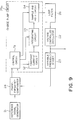
- the PLL frequency synthesizer is similar in structure and operation to the conventional PLL frequency synthesizer except that the PLL frequency synthesizer further comprises a switch 65, a reset circuit 66, a control circuit 70, and a digital-analog converter 71.
- the control circuit 70 is supplied with the designated dividing number D, the divided signal, the phase-frequency difference signal. On changing the output frequency, the control circuit 70 produces first and second control signals. The control circuit 70 also produces voltage data on changing the output frequency. The voltage data represents a control voltage which is defined by the designated dividing number D on the basis of the phase-frequency difference signal. The control circuit 70 determines the voltage data by carrying out binary search on the phase-frequency difference signal.
- the switch 65 is inserted between the loop filter 26 and the voltage controlled oscillator 22.
- the switch 65 is supplied with the first control signal.
- the switch 65 switches off in response to the first control signal.
- the loop filter 26 comprises first and second resistors 261 and 262 and a filter capacitor 263.
- the first resistor 261 has one end connected to the charge pump circuit 25 and has another end connected to the switch 65 and to one end of the second resistor.
- the second resistor 262 has another end connected to one end of the filter capacitor 263 which has another end grounded.
- the digital-analog converter 71 is supplied with the voltage data from the control circuit 70.
- the digital-analog converter 71 is activated only when the output frequency is changed.
- the digital-analog converter 71 converts the voltage data into the control voltage.
- the control voltage is supplied to the voltage controlled oscillator 22 and the filter capacitor 263 of the loop filter 26.
- the charge pump circuit 25 Responsive to the second control signal, the charge pump circuit 25 is unactivated or put into a high impedance state.
- the reset circuit 66 is inserted between the reference signal generator 29 and the phase-frequency comparator 24.
- the control circuit 70 controls the reset circuit 66 so as to make the reset circuit 66 produce a reset signal which has a phase equal to that of the divided signal.
- the reset signal is supplied to the phase-frequency comparator 24 instead of the reference signal.
- the digital-analog converter 71 supplies the control voltage to both of the voltage controlled oscillator 22 and the filter capacitor 263 of the loop filter 26.
- the digital-analog converter 71 may be modified into first and second digital-analog converters 71 and 72 as shown in Fig. 14. Under the circumstances, the first digital-analog converter 71 supplies the control voltage to the voltage controlled oscillator 22.
- the second digital-analog converter 72 supplies the control voltage to the filter capacitor 263 of the loop filter 26.
Landscapes
- Stabilization Of Oscillater, Synchronisation, Frequency Synthesizers (AREA)
Abstract
Description
- This invention relates to a frequency synthesizer with a phase-locked loop (PLL). Such a frequency synthesizer is called a PLL frequency synthesizer.
- As well known in the art, the PLL frequency synthesizer comprises a reference signal generator, a voltage controlled oscillator, a variable frequency divider, a phase-frequency comparator, and a control voltage supplying circuit. The reference signal generator generates a reference signal with a reference frequency. Responsive to a control voltage signal, the voltage controlled oscillator generates a voltage controlled signal having a controllable oscillating frequency. The PLL frequency synthesizer produces the voltage controlled signal as an output signal. Therefore, the output signal has an output frequency equal to the controllable oscillating frequency. The output signal is supplied to the variable frequency divider. The variable frequency divider is also supplied with a designated dividing number D which defines the output frequency, where D represents a positive integer. The variable frequency divider frequency divides the output signal on the basis of the designated dividing number D to produce a divided signal. In other words, the variable frequency divider is for frequency dividing the output signal by a factor l/D. The phase-frequency comparator is supplied with the reference signal and the divided signal. The phase-frequency comparator detects a phase-frequency difference between the reference signal and the divided signal to produce a phase-frequency difference signal indicative of the phase-frequency difference. In other words, the phase-frequency difference signal indicates one of lag and lead phases which the divided signal has in comparison with the reference signal. Responsive to the phase-frequency difference signal, the control voltage supplying circuit supplies the control voltage signal to the voltage controlled oscillator.
- More specifically, the control voltage supplying circuit comprises a current flow control circuit and a loop filter. Responsive to the phase-frequency difference signal, the current flow control circuit controls flow-in and flow-out of current supplied therefrom/to to produce a current flow control signal. The current flow control signal indicates the flow-out of the current when the phase-frequency difference signal indicates the lag phase. The current flow control signal indicates the flow-in of the current when the phase-frequency difference signal indicates the lead phase. Supplied with the current flow control signal, the loop filter filters the current flow control signal into a filtered signal as the control voltage signal. More particularly, the loop filter comprises a filter capacitor which is selectively charged and discharged when the current flow control signal indicates the flow-out and the flow-in of the current, respectively.
- In a conventional PLL frequency synthesizer, changing of the output frequency is carried out by changing step by step the designated dividing number D. Therefore, the PLL frequency synthesizer has a variable delay amount on changing the output frequency. As a result, a frequency error of the output frequency occurs in the PLL frequency synthesizer on changing the output frequency. Accordingly, the conventional PLL frequency synthesizer is defective in that it is impossible to change the output frequency at a high speed.
- It is therefore an object of the present invention to provide a PLL frequency synthesizer which is capable of changing an output frequency at a high speed.
- Other objects of this invention will become clear as the description proceeds.
- According to a first aspect of this invention, a frequency synthesizer comprises a reference signal generator for generating a reference signal with a reference frequency, a voltage controlled oscillator responsive to a control voltage signal for generating an output signal having an output frequency, a variable frequency divider supplied with the output signal and responsive to a designated dividing number defining the output frequency for frequency dividing the output signal on the basis of the designated dividing number to produce a divided signal, a first pulse removing circuit supplied with the reference signal and responsive to first removing data indicative of a first pulse number for removing pulses from the reference signal that are equal in number to the first pulse number for a first predetermined cycle to produce a first pulse removed signal, a second pulse removing circuit supplied with the divided signal and responsive to second removing data indicative of a second pulse number for removing pulses from the divided signal that are equal in number to the second pulse number for a second predetermined cycle to produce a second pulse removed signal, a phase-frequency comparator supplied with the first and the second pulse removed signals for detecting a phase-frequency difference between the first and the second pulse removed signals to produce a phase-frequency difference signal indicative of the phase-frequency difference, and a control voltage supplying circuit supplied with the phase-frequency difference signal for supplying the control voltage signal to the voltage controlled oscil-ator in response to the phase-frequency difference signal.
- According to a second aspect of this invention, a frequency synthesizer comprises a reference signal generator for generating a reference signal with a reference frequency, a voltage controlled oscillator responsive to a control voltage signal for generating an output signal having an output frequency, a variable frequency divider supplied with the output signal and responsive to a designated dividing number defining the output frequency for frequency dividing the output signal on the basis of the designated dividing number to produce a divided signal, a phase-frequency comparator supplied with the reference signal and the divided signal for detecting a phase-frequency difference between the reference signal and the divided signal to produce a phase-frequency difference signal indicating one of lag and lead phases which the divided signal has in comparison with the reference signal, a current flow control circuit responsive to the phase-frequency difference signal for controlling flow-in and flow-out of current supplied therefrom/to to produce a current flow control signal, a loop filter supplied with the current flow control signal for filtering the current flow control signal into a filtered signal as the control voltage signal, and a current controlling circuit responsive to a current command for controlling the current supplied from/to the current flow control circuit.
- According to a third aspect of this invention, a frequency synthesizer comprises a reference signal generator for generating a reference signal with a reference frequency, a voltage controlled oscillator responsive to a control voltage signal for generating an output signal having an output frequency, a variable frequency divider supplied with the output signal and responsive to a designated dividing number defining the output frequency for frequency dividing the output signal on the basis of the designated dividing number to produce a divided signal, a phase-frequency comparator supplied with the reference signal and the divided signal for detecting a phase-frequency difference between the reference signal and the divided signal to produce a phase-frequency difference signal indicating one of lag and lead phases which the divided signal has in comparison with the reference signal, a current flow control circuit responsive to the phase-frequency difference signal for controlling flow-in and flow-out of current supplied therefrom/to to produce a current flow control signal, and a loop filter supplied with the current flow control signal for filtering the current flow control signal into a filtered signal as the control voltage signal. The above-mentioned current flow control circuit comprises a control circuit responsive to the phase-frequency difference signal for producing first through third control signals, a constant current circuit responsive to the first control signal for producing a constant current, an integrating circuit having an initial voltage for integrating the constant current to an integrated voltage, the integrating circuit being reset from the integrated voltage to the initial voltage in response to the second control signal, and a sample and hold circuit responsive to the third control signal for sampling the integrated voltage to hold a sampled voltage as a held signal, the sample and hold circuit producing the held signal as the current flow control signal.
- According to a fourth aspect of this invention, a frequency synthesizer comprises a reference signal generator for generating a reference signal with a reference frequency, a voltage controlled oscillator responsive to a control voltage signal for generating an output signal having an output frequency, a variable frequency divider supplied with the output signal and responsive to a designated dividing number defining the output frequency for frequency dividing the output signal on the basis of the designated dividing number to produce a divided signal, a phase-frequency comparator supplied with the reference signal and the divided signal for detecting a phase-frequency difference between the reference signal and the divided signal to produce a phase-frequency difference signal indicative of the phase-frequency difference, modifying means connected to the phase-frequency comparator and responsive to a control enable signal for modifying the phase-frequency difference signal into a modified signal, and a control voltage supplying circuit supplied with the modified signal for supplying the control voltage signal to the voltage controlled oscillator in response to the modified signal.
- According to a fifth aspect of this invention, a frequency synthesizer comprises a reference signal generator for generating a reference signal with a reference frequency, a voltage controlled oscillator responsive to a control voltage signal for generating an output signal having an output frequency, a variable frequency divider supplied with the output signal and responsive to a designated dividing number defining the output frequency for frequency dividing the output signal on the basis of the designated dividing number to produce a divided signal, a phase-frequency comparator supplied with the reference signal and the divided signal for detecting a phase-frequency difference between the reference signal and the divided signal to produce a phase-frequency difference signal indicative of the phase-frequency difference, a current flow control circuit responsive to the phase-frequency difference signal for controlling flow-in and flow-out of current therefrom/to to produce a current flow control signal, a loop filter supplied with the current flow control signal for filtering the current flow control signal into a filtered signal, the loop filter comprising a filter capacitor which is selectively charged and discharged in accordance with the current flow control signal, a control circuit supplied with the phase-frequency difference signal and the designated dividing number for producing a control signal and voltage data on changing the output frequency, the voltage data representing a control voltage which is defined by the designated dividing number on the basis of the phase-frequency difference signal, a switch inserted between the loop filter and the voltage controlled oscillator for switching off in response to the control signal, and a digital-analog converter supplied with the voltage data for converting the voltage data into the control voltage, the digital-analog converter supplying the control voltage to the voltage controlled oscillator and the filter capacitor of the loop filter.
-
- Fig. 1 is a block diagram of a conventional PLL frequency synthesizer;
- Fig. 2 is a block diagram of a PLL frequency synthesizer according to a first embodiment of the instant invention;
- Fig. 3 is a block diagram of a pulse removing circuit for use in the PLL frequency synthesizer illustrated in Fig. 2;
- Figs. 4(a) through (e) collectively show a time chart for use in describing operation of the pulse removing circuit illustrated in Fig. 3;
- Fig. 5 is a block diagram of a PLL frequency synthesizer according to a second embodiment of the instant invention;
- Fig. 6 is a block diagram of a charge pump circuit for use in the PLL frequency synthesizer illustrated in Fig. 5;
- Fig. 7 is a block diagram of a charge-up control circuit of a current controlling circuit for use in the PLL frequency synthesizer illustrated in Fig. 5;
- Figs. 8(a) through (c) collectively show a time chart for use in describing operation of the charge-up control circuit illustrated in Fig. 7;
- Fig. 9 is a block diagram of a PLL frequency synthesizer according to a third embodiment of the instant invention;
- Fig. 10 shows a time chart for use in describing operation of a charge pump circuit of the PLL frequency synthesizer illustrated in Fig. 9;
- Fig. 11 is a block diagram of a PLL frequency synthesizer according to a fourth embodiment of the instant invention;
- Fig. 12 shows a time chart for use in describing operation of the PLL frequency synthesizer illustrated in Figs. 1 and 11;
- Fig. 13 is a block diagram of a PLL frequency synthesizer according to a fifth embodiment of the instant invention; and
- Fig. 14 shows a block diagram of a PLL frequency synthesizer which modifies the PLL frequency synthesizer illustrated in Fig. 12.
- Referring to Fig. 1, a conventional PLL frequency synthesizer will be described at first in order to facilitate an understanding of the present invention.
- The PLL frequency synthesizer comprises a
reference signal generator 21, a voltage controlledoscillator 22, avariable frequency divider 23, a phase-frequency comparator 24, acharge pump circuit 25, and aloop filter 26. - The
reference signal generator 21 generates a reference signal with a reference frequency. The voltage controlledoscillator 22 is supplied with a control voltage signal in the manner which will become clear as the description proceeds. Responsive to the control voltage signal, the voltage controlledoscillator 22 generates a voltage controlled signal having a controllable oscillating frequency. The PLL frequency synthesizer produces the voltage controlled signal as an output signal. Therefore, the output signal has an output frequency equal to the controllable oscillating frequency. - The output signal is supplied to the
variable frequency divider 23. Thevariable frequency divider 23 is also supplied with a designated dividing number D which defines the output frequency, where D represents a positive integer. Thevariable frequency divider 23 frequency divides the output signal on the basis of the designated dividing number D to produce a divided signal. In other words, thevariable frequency divider 23 is for frequency dividing the output signal by a factor l/D. The phase-frequency comparator 24 is supplied with the reference signal and the divided signal. The phase-frequency comparator 24 detects a phase-frequency difference between the reference signal and the divided signal to produce a phase-frequency difference signal indicative of the phase-frequency difference. In other words, the phase-frequency difference signal indicates one of lag and lead phases which the divided signal has in comparison with the reference signal. - The phase-frequency difference signal is supplied with the
charge pump circuit 25. Thecharge pump circuit 25 acts as a current flow control circuit which is for controlling flow-in and flow-out of current supplied therefrom/to to produce a current flow control signal. The current flow control signal indicates the flow-out of the current when the phase-frequency difference signal indicates the lag phase. The current flow control signal indicates the flow-in of the current when the phase-frequency difference signal indicates the lead phase. The current flow control signal is supplied with theloop filter 26. The loop filter filters the current flow control signal into a filtered signal as the control voltage signal. More particularly, theloop filter 26 comprises a filter capacitor (not shown) which is selectively charged and discharged when the current flow control signal indicates the flow-out and the flow-in of the current, respectively. At any rate, a combination of thecharge pump circuit 25 and theloop filter 26 serves as a control voltage supplying circuit for supplying the control voltage signal to the voltage controlled oscillator in response to the phase-frequency difference signal. - As apparent from the above description, the PLL frequency synthesizer produces the output signal having the output frequency which is equal to D times as large as the reference frequency of the reference signal. It is therefore possible to change the output frequency by changing the designated dividing number D. In the conventional PLL frequency synthesizer, changing of the output frequency is carried out by changing step by step the designated dividing number D. As a result, the conventional PLL frequency synthesizer is defective in that it is impossible to change the output frequency at a high speed, as mentioned in the preamble of the instant specification.
- Referring to Fig. 2, the description will proceed to a PLL frequency synthesizer according to a first embodiment of this invention. The PLL frequency synthesizer is similar in structure and operation to the conventional PLL frequency synthesizer illustrated in Fig. 1 except that the PLL frequency synthesizer further comprises first and second
pulse removing circuits - The first
pulse removing circuit 31 is connected between thereference signal generator 21 and the phase-frequency comparator 24. The secondpulse removing circuit 32 is connected between thevariable frequency divider 23 and the phase-frequency comparator 24. - The first
pulse removing circuit 31 is supplied with the reference signal from thereference signal generator 21 and first removing data A1 indicative of a first pulse number. Responsive to the first removing data A1, the firstpulse removing circuit 31 removes pulses from the reference signal that are equal in number to the first pulse number for a first predetermined cycle to produce a first pulse removed signal. Instead of the reference signal, the first pulse removed signal is supplied to the phase-frequency comparator 24. - The second
pulse removing circuit 32 is supplied with the divided signal from thevariable frequency divider 23 and second removing data A2 indicative of a second pulse number. The secondpulse removing circuit 32 removes pulses from the divided signal that are equal in number to the second pulse number for a second predetermined cycle to produce a second pulse removed signal. Instead of the divided signal, the second pulse removed signal is supplied to the phase-frequency comparator 24. - Therefore, the phase-
frequency comparator 24 detects a phase-frequency difference between the first and the second pulse removed signals to produce a phase-frequency difference signal indicative of the phase-frequency difference. - Turning to Fig. 3, the first
pulse removing circuit 31 comprises afirst inverter 311, afirst counter 312, and a first ANDgate 313. Thefirst inverter 311 is supplied with the reference signal from the reference signal generator 21 (Fig. 2) as a first input pulse signal. Thefirst inverter 311 inverts the first input pulse signal to produce a first inverted pulse signal. Thefirst inverter 311 is connected to thefirst counter 312 which is supplied with the first pulse removing data. Thefirst counter 312 counts up a first count in synchronism with the first inverted pulse signal. Thefirst counter 312 produces a first time-up signal when the first count increases up to the first pulse number. The first time-up signal is supplied to the first ANDgate 313 which is supplied with the first input pulse signal. Responsive to the first input pulse signal and the first time-up signal, the first ANDgate 313 produces a first AND'ed signal as the first pulse removed signal. - Similarly, the second
pulse removing circuit 32 comprises asecond inverter 321, asecond counter 322, and a second ANDgate 323. Thesecond inverter 321 is supplied with the divided signal from the variable frequency divider 23 (Fig. 2) as a second input pulse signal. Thesecond inverter 321 inverts the second input pulse signal to produce a second inverted pulse signal. Thesecond inverter 321 is connected to thesecond counter 322 which is supplied with the second pulse removing data. Thesecond counter 322 counts up a second count in synchronism with the second inverted pulse signal. Thesecond counter 322 produces a second time-up signal when the second count increases up to the second pulse number. The second time-up signal is supplied to the second ANDgate 323 which is supplied with the second input pulse signal. Responsive to the second input pulse signal and the second time-up signal, the second ANDgate 323 produces a second AND'ed signal as the second pulse removed signal. - Turning to Figs. 4(a) through (e), description will be made as regards operation of the first
pulse removing circuit 31. The first input pulse signal is depicted along Fig. 4(a). The first input pulse signal is inverted by thefirst inverter 311 into the first inverted pulse signal as shown in Fig. 4(b). Thefirst inverter 311 has an inverting delay time denoted to d1. - It will be assumed that the
first counter 312 is supplied with the first pulse removing data indicative of the first pulse number equal to four. In this event, thefirst counter 312 counts up the first count at a leading edge of each pulse in the first inverted pulse signal. Thefirst counter 312 produces the first time-up signal of a logical "1" level when the first count increases up to the first pulse number, namely, four, as shown in Fig. 4(c). Thefirst counter 312 is reset to produce the first time-up signal of a logical "0" level in response to another leading edge of the next succeeding pulse of the first inverted pulse signal. Thefirst counter 312 has a counting delay time denoted to d2. Under the circumstances, the first ANDgate 313 produces the first AND'ed signal as the first pulse removed signal as shown in Fig. 4(d). That is, the first ANDgate 313 produces the first pulse removed signal having pulses which is one-fifth as large as those of the first input pulse signal. In other words, the firstpulse removing circuit 31 removes four pulses from the reference signal for the first predetermined cycle which has five pulses. The first ANDgate 313 has a gate delay time denoted to d3. - If the first pulse removing data indicates the first pulse number equal to zero, the
first counter 312 continuously produces the first time-up signal with the logical "1" level. In this event, the first ANDgate 313 produces the first pulse removed signal to which the first input pulse signal is delayed for the gate delay time t3 by the first ANDgate 313 as shown in Fig. 4(e). - Operation of the second
pulse removing circuit 32 is similar to that of the firstpulse removing circuit 31 and the description thereof is therefore omitted. - Referring to Fig. 5, the description will proceed to a PLL frequency synthesizer according to a second embodiment of this invention. The PLL frequency synthesizer is similar in structure and operation to the conventional PLL frequency synthesizer illustrated in Fig. 1 except that the PLL frequency synthesizer further comprises a current
controlling circuit 35. - The current
controlling circuit 35 is connected to thecharge pump circuit 25 and is supplied with a current command C. Responsive to the current command C, the currentcontrolling circuit 35 controls the current for thecharge pump circuit 25. More specifically, the current command C is present while the output frequency is changed. The currentcontrolling circuit 35 controls the current so as to increase the current when the current command C is present and then to gradually decrease the current after the current command C becomes absent. A little more in detail, the currentcontrolling circuit 35 comprises a charge-up control circuit and a discharge control circuit. - Turning to Fig. 6, the
charge pump circuit 25 comprises a complementary-symmetry metal-oxide-semiconductor field-effect transistor (CMOSFET) which consists of a p-channel MOSFET 36 and an n-channel MOSFET 37. Each of theMOSFETs channel MOSFETs channel MOSFET 36 has the source terminal which is connected to the charge-up control circuit of the currentcontrolling circuit 35. The n-channel MOSFET 37 has the source terminal which is connected to the discharge control circuit of the currentcontrolling circuit 35. Both of the p-channel and the n-channel MOSFETs channel MOSFET 36. The lead phase signal is supplied to the gate terminal of the n-channel MOSFET 37. - Supplied with the lag phase signal, the p-
channel MOSFET 36 is put into an ON state, thereby the current flows from the charge-up control circuit to theloop filter 26 through the p-channel MOSFET 36. Supplied with the lead phase signal, the n-channel MOSFET 37 is put into an ON state, thereby the current flows from theloop filter 26 to the discharge control circuit through the n-channel MOSFET 37. - Turning to Fig. 7, the charge-up control circuit of the current
controlling circuit 36 comprises a switchingelement 41, anoperational amplifier 42, an n-channel MOSFET 43, first and second p-channel MOSFETs third resistors capacitor 49. Theoperational amplifier 42 has an inverting input terminal, a noninverting input terminal, and an amplifier output terminal. - The switching
element 41 has a control input terminal supplied with the current command C. The switchingelement 41 is supplied with a positive source voltage +VDD. The switchingelement 41 is connected to the noninverting input terminal of theoperational amplifier 42. When the current command C is present or has a logic one value, the switchingelement 41 turns on, thereby the positive source voltage +VDD is supplied to the noninverting input terminal of theoperational amplifier 42. The inverting input terminal of theoperational amplifier 42 is an end of thefirst resistor 46 which has another end grounded. The noninverting input terminal of theoperational amplifier 42 is connected to an end of thesecond resistor 47 which has another end grounded. Thesecond resistor 47 is connected to thecapacitor 49 in parallel. The noninverting input terminal of theoperational amplifier 42 is also connected to an end of thethird resistor 47 which has another end supplied with the positive source voltage +VDD. The amplifier output terminal of theoperational amplifier 42 is connected to the gate terminal of the n-channel MOSFET 43 which has the source terminal connected to the inverting input terminal of theoperational amplifier 42. - The n-
channel MOSFET 43 has the drain terminal which is connected to the drain terminal of the first p-channel MOSFET 44. The drain terminal of the n-channel MOSFET 43 is also connected to the gate terminals of the first and the second p-channel MOSFETs channel MOSFETs channel MOSFET 45 has the drain terminal which is connected to the source terminal of the p-channel MOSFET 36 (Fig. 6). Therefore, a combination of the first and the second p-channel MOSFETs channel MOSFET 45 has a gate width which is N times as large as that of the first p-channel MOSFET 44, where N represents a predetermined number. When a first drain current D1 flows through the n-channel MOSFET 43, through the second p-channel MOSFET 45 flows a second drain current D2 which is N times as large as the first drain current D1. - Turning to Figs. 8(a) through (c), description will be made as regards operation of the charge-up control circuit of the current
controlling circuit 36 illustrated in Fig. 7. It will be assumed that the first through thethird resistors 46 to 48 have first through third resistance values, respectively, which are denoted to R46, R47, and R48. The third resistance value R48 is larger than the second resistance value R47. Figs. 8(a) through (c) show the current command C, and the first and the second drain currents D1 and D2, respectively. - When the current command C is present or becomes the logic one value at a time instant t0, the switching
element 41 turns on. Therefore, thecapacitor 49 is charged up to a voltage of VDD. Through the n-channel MOSFET 43 flows the first drain current D1 which has a current value of VDD/R46. Therefore, through the second p-channel MOSFET 45 flows the second drain current D2 which has a current value of
- When the current command C becomes absent or the logic zero value at a time instant t1, the switching
element 41 turns off. Therefore, thecapacitor 49 is exponentially discharged up to a voltage of


- The discharge control circuit of the current
controlling circuit 35 is similar in structure and operation to the charge-up control circuit illustrated in Fig. 7 except that the n-channel MOSFET 43 is replaced with a p-channel MOSFET, the p-channel MOSFETs - Referring to Fig. 9, the description will proceed to a PLL frequency synthesizer according to a third embodiment of this invention. The PLL frequency synthesizer is similar in structure and operation to the conventional PLL frequency synthesizer illustrated in Fig. 1 except that the charge pump circuit is modified from that illustrated in Fig. 1 as will later become clear. The charge pump circuit is therefore depicted at 25a.
- The illustrated
charge pump circuit 25a comprises acontrol circuit 51, a constantcurrent circuit 52, an integratingcircuit 53, and a sample and holdcircuit 54. - The
control circuit 51 is connected to the phase-frequency comparator 24. Responsive to the phase-frequency difference signal, thecontrol circuit 51 produces first through third control signals. The first through the third control signals are supplied to the constantcurrent circuit 52, the integratingcircuit 53, and the sample and holdcircuit 54, respectively. - Responsive to the first control signal, the constant
current circuit 52 produces a constant current. The constant current is supplied to the integratingcircuit 53. The integratingcircuit 53 has an initial voltage. The integratingcircuit 53 integrates the constant current to an integrated voltage. The integratingcircuit 53 is reset from the integrated voltage to the initial voltage in response to the second control signal. The integrated voltage is supplied to the sample and holdcircuit 54. Responsive to the third control signal, the sample and holdcircuit 44 samples the integrated voltage to hold a sampled voltage as a held signal. The sample and holdcircuit 44 supplies the held signal to theloop filter 26 as the current flow control signal. - Referring to Fig. 10 in addition to Fig. 9, description will be made as regards operation of the
charge pump circuit 25a. In Fig. 10, the lag phase signal, the constant current, the integrated voltage, and the held signal are depicted along first through fourth lines. - As shown in the first line in Fig. 10, the lag phase signal is supplied from the phase-
frequency comparator 24 to thecontrol circuit 51 during a first time duration between a first time instant t1 and a second time instant t2. Under the circumstances, thecontrol circuit 51 produces the first control signal during a second time duration between the first time instant t1 and a third time instant t3. Responsive to the first control signal, the constantcurrent circuit 52 produces the constant current during the second time duration as shown in the second line in Fig. 10. Therefore, the integratingcircuit 53 integrates the constant current to the integrated voltage during the second time duration as shown in the third line in Fig. 10. After the third time instant t3, the integratingcircuit 53 keeps the integrated voltage. At a fourth time instant t4, thecontrol circuit 51 produces the third control signal. Responsive to the third control signal, the sample and holdcircuit 44 samples the integrated voltage to hold a sampled voltage as a held signal at a fifth time instant t5. The held signal is supplied to theloop filter 26 as the current flow control signal. At a sixth time instant t6, thecontrol circuit 51 produces the second control signal. Responsive to the second control signal, the integratingcircuit 53 is reset from the integrated voltage to the initial voltage. Therefore, thecharge pump circuit 25a increases a level of the current flow control signal in response to the lag phase signal. In the similar operation, thecharge pump circuit 25a decreases the level of the current flow control signal in response to the lead phase signal. - It is understood that it is possible to set a desired value to a gain of the
charge pump circuit 25a by changing the ratio of the first time duration to the second time duration. - Referring to Fig. 11, the description will proceed to a PLL frequency synthesizer according to a fourth embodiment of this invention. The PLL frequency synthesizer is similar in structure and operation to the conventional PLL frequency synthesizer illustrated in Fig. 1 except that the PLL frequency synthesizer further comprises a
control circuit 60. - The
control circuit 60 is connected between the phase-frequency comparator 24 and thecharge pump circuit 25. Thecontrol circuit 60 is supplied with a control enable signal CE. Responsive to the control enable signal CE, thecontrol circuit 60 acts as a modifying arrangement for modifying the phase-frequency difference signal into a modified signal. Instead of the phase-frequency difference signal, the modified signal is supplied to thecharge pump circuit 25. Therefore, thecharge pump circuit 25 controls, in response to the modified signal, flow-in and flow-out of the current supplied therefrom/to to produce the current flow control signal. A little more in detail, thecontrol circuit 60 is operable in one of a first mode and a second mode. At first, the first mode will be described. The second mode will be described later in the following. - In the first mode, the control enable signal CE is present while the output frequency is changed. The phase-frequency difference signal comprises a pulse sequence having pulses for a predetermined cycle that are equal in number to a controllable number. When the control enable signal CE is present, the
control circuit 60 gradually decreases the controllable number until at last a predetermined final number. The predetermined final number is, for example, one sixty-fourths as large as the controllable number before being decreased. - Fig. 12 shows transient responses of the output frequency in the conventional PLL frequency synthesizer (Fig. 1) and the PLL frequency synthesizer according to the fourth embodiment. In Fig. 12, a transient response for the conventional PLL frequency synthesizer is depicted at a solid line. Another transient response for the PLL frequency synthesizer according to the fourth embodiment is depicted at a dotted line. As apparent from Fig. 12, it is possible to raise up the transient response by decreasing the controllable number.
- In the second mode, the control enable signal CE is present in a steady state of the PLL frequency synthesizer. The phase-frequency difference signal comprises a pulse sequence having pulses each of which has a controllable pulse width. The
control circuit 60 narrows the controllable pulse width when the control enable signal CE is present. It is possible to improve unstableness in the PLL frequency synthesizer. - Referring to Fig. 13, the description will proceed to a PLL frequency synthesizer according to a fifth embodiment of this invention. The PLL frequency synthesizer is similar in structure and operation to the conventional PLL frequency synthesizer except that the PLL frequency synthesizer further comprises a
switch 65, areset circuit 66, acontrol circuit 70, and a digital-analog converter 71. - The
control circuit 70 is supplied with the designated dividing number D, the divided signal, the phase-frequency difference signal. On changing the output frequency, thecontrol circuit 70 produces first and second control signals. Thecontrol circuit 70 also produces voltage data on changing the output frequency. The voltage data represents a control voltage which is defined by the designated dividing number D on the basis of the phase-frequency difference signal. Thecontrol circuit 70 determines the voltage data by carrying out binary search on the phase-frequency difference signal. - The
switch 65 is inserted between theloop filter 26 and the voltage controlledoscillator 22. Theswitch 65 is supplied with the first control signal. Theswitch 65 switches off in response to the first control signal. - The
loop filter 26 comprises first andsecond resistors filter capacitor 263. Thefirst resistor 261 has one end connected to thecharge pump circuit 25 and has another end connected to theswitch 65 and to one end of the second resistor. Thesecond resistor 262 has another end connected to one end of thefilter capacitor 263 which has another end grounded. - The digital-
analog converter 71 is supplied with the voltage data from thecontrol circuit 70. The digital-analog converter 71 is activated only when the output frequency is changed. The digital-analog converter 71 converts the voltage data into the control voltage. The control voltage is supplied to the voltage controlledoscillator 22 and thefilter capacitor 263 of theloop filter 26. - Responsive to the second control signal, the
charge pump circuit 25 is unactivated or put into a high impedance state. - The
reset circuit 66 is inserted between the reference signal generator 29 and the phase-frequency comparator 24. On the basis of the divided signal, thecontrol circuit 70 controls thereset circuit 66 so as to make thereset circuit 66 produce a reset signal which has a phase equal to that of the divided signal. The reset signal is supplied to the phase-frequency comparator 24 instead of the reference signal. - In the PLL frequency synthesizer illustrated in Fig. 13, the digital-
analog converter 71 supplies the control voltage to both of the voltage controlledoscillator 22 and thefilter capacitor 263 of theloop filter 26. The digital-analog converter 71 may be modified into first and second digital-analog converters analog converter 71 supplies the control voltage to the voltage controlledoscillator 22. The second digital-analog converter 72 supplies the control voltage to thefilter capacitor 263 of theloop filter 26.
Claims (11)
- A frequency synthesizer comprising:a reference signal generator for generating a reference signal with a reference frequency;a voltage controlled oscillator responsive to a control voltage signal for generating an output signal having an output frequency;a variable frequency divider supplied with said output signal and responsive to a designated dividing number defining said output frequency for frequency dividing said output signal on the basis of said designated dividing number to produce a divided signal;a first pulse removing circuit supplied with said reference signal and responsive to first removing data indicative of a first pulse number for removing pulses from said reference signal that are equal in number to said first pulse number for a first predetermined cycle to produce a first pulse removed signal;a second pulse removing circuit supplied with said divided signal and responsive to second removing data indicative of a second pulse number for removing pulses from said divided signal that are equal in number to said second pulse number for a second predetermined cycle to produce a second pulse removed signal;a phase-frequency comparator supplied with said first and said second pulse removed signals for detecting a phase-frequency difference between said first and said second pulse removed signals to produce a phase-frequency difference signal indicative of said phase-frequency difference; anda control voltage supplying circuit supplied with said phase-frequency difference signal for supplying said control voltage signal to said voltage controlled oscillator in response to said phase-frequency difference signal.
- A frequency synthesizer as claimed in Claim 1, wherein said first pulse removing circuit comprises:a first inverter supplied with said reference signal as a first input pulse signal for inverting said first input pulse signal to produce a first inverted pulse signal;a first counter connected to said first inverter and supplied with said first pulse removing data for counting up a first count in synchronism with said first inverted pulse signal, said first counter producing a first time-up signal when said first count increases up to said first pulse number; anda first AND gate responsive to said first input pulse signal and said first time-up signal for producing a first AND'ed signal as said first pulse removed signal.
- A frequency synthesizer as claimed in Claim 1, wherein said second pulse removing circuit comprises:a second inverter supplied with said divided signal as a second input pulse signal for inverting said second input pulse signal to produce a second inverted pulse signal;a second counter connected to said second inverter and supplied with said second pulse removing data for counting up a second count in synchronism with said second inverted pulse signal, said second counter producing a second time-up signal when said second count increases up to said second pulse number; anda second AND gate responsive to said second input pulse signal and said second time-up signal for producing a second AND'ed signal as said second pulse removed signal.
- A frequency synthesizer comprising:a reference signal generator for generating a reference signal with a reference frequency;a voltage controlled oscillator responsive to a control voltage signal for generating an output signal having an output frequency;a variable frequency divider supplied with said output signal and responsive to a designated dividing number defining said output frequency for frequency dividing said output signal on the basis of said designated dividing number to produce a divided signal;a phase-frequency comparator supplied with said reference signal and said divided signal for detecting a phase-frequency difference between said reference signal and said divided signal to produce a phase-frequency difference signal indicating one of lag and lead phases which said divided signal has in comparison with said reference signal;a current flow control circuit responsive to said phase-frequency difference signal for controlling flow-in and flow-out of current supplied therefrom/to to produce a current flow control signal;a loop filter supplied with said current flow control signal for filtering said current flow control signal into a filtered signal as said control voltage signal; anda current controlling circuit responsive to a current command for controlling said current supplied from/to said current flow control circuit.
- A frequency synthesizer as claimed in Claim 4, said current command being present while said controllable oscillating frequency is changed, wherein said current controlling circuit controls said current so as to increase said current when said current command is present and then to gradually decrease said current after the current command becomes absent.
- In a frequency synthesizer comprising a reference signal generator for generating a reference signal with a reference frequency, a voltage controlled oscillator responsive to a control voltage signal for generating an output signal having an output frequency, a variable frequency divider supplied with said output signal and responsive to a designated dividing number defining said output frequency for frequency dividing said output signal on the basis of said designated dividing number to produce a divided signal, a phase-frequency comparator supplied with said reference signal and said divided signal for detecting a phase-frequency difference between said reference signal and said divided signal to produce a phase-frequency difference signal indicating one of lag and lead phases which said divided signal has in comparison with said reference signal, a current flow control circuit responsive to said phase-frequency difference signal for controlling flow-in and flow-out of current supplied therefrom/to to produce a current flow control signal, and a loop filter supplied with said current flow control signal for filtering said current flow control signal into a filtered signal as said control voltage signal, the improvement wherein said current flow control circuit comprises:a control circuit responsive to said phase-frequency difference signal for producing first through third control signals;a constant current circuit responsive to said first control signal for producing a constant current;an integrating circuit having an initial voltage for integrating said constant current to an integrated voltage, said integrating circuit being reset from said integrated voltage to said initial voltage in response to said second control signal; anda sample and hold circuit responsive to said third control signal for sampling said integrated voltage to hold a sampled voltage as a held signal, said sample and hold circuit producing said held signal as said current flow control signal.
- A frequency synthesizer comprising:a reference signal generator for generating a reference signal with a reference frequency;a voltage controlled oscillator responsive to a control voltage signal for generating an output signal having an output frequency;a variable frequency divider supplied with said output signal and responsive to a designated dividing number defining said output frequency for frequency dividing said output signal on the basis of said designated dividing number to produce a divided signal;a phase-frequency comparator supplied with said reference signal and said divided signal for detecting a phase-frequency difference between said reference signal and said divided signal to produce a phase-frequency difference signal indicative of said phase-frequency difference;modifying means connected to said phase-frequency comparator and responsive to a control enable signal for modifying said phase-frequency difference signal into a modified signal; anda control voltage supplying circuit supplied with said modified signal for supplying said control voltage signal to said voltage controlled oscillator in response to said modified signal.
- A frequency synthesizer as claimed in Claim 7, said control enable signal being present while said controllable oscillating frequency is changed, said phase-frequency difference signal comprising a pulse sequence having pulses for a predetermined cycle that are equal in number to a controllable number, wherein said modifying means gradually decreases said controllable number until at last a predetermined final number when said control enable signal is present.
- A frequency synthesizer as claimed in Claim 7, said phase-frequency difference signal comprising a pulse sequence having pulses each of which has a controllable pulse width, wherein said modifying means narrows said controllable pulse width in response to said control enable signal.
- A frequency synthesizer comprising:a reference signal generator for generating a reference signal with a reference frequency;a voltage controlled oscillator responsive to a control voltage signal for generating an output signal having an output frequency;a variable frequency divider supplied with said output signal and responsive to a designated dividing number defining said output frequency for frequency dividing said output signal on the basis of said designated dividing number to produce a divided signal;a phase-frequency comparator supplied with said reference signal and said divided signal for detecting a phase-frequency difference between said reference signal and said divided signal to produce a phase-frequency difference signal indicative of said phase-frequency difference;a current flow control circuit responsive to said phase-frequency difference signal for controlling flow-in and flow-out of current supplied therefrom/to to produce a current flow control signal;a loop filter supplied with said current flow control signal for filtering said current flow control signal into a filtered signal, said loop filter comprising a filter capacitor which is selectively charged and discharged in accordance with said current flow control signal;a control circuit supplied with said phase-frequency difference signal and said designated dividing number for producing a control signal and voltage data on changing the output frequency, said voltage data representing a control voltage which is defined by said designated dividing number on the basis of said phase-frequency difference signal;a switch inserted between said loop filter and said voltage controlled oscillator for switching off in response to said control signal; anda digital-analog converter supplied with said voltage data for converting said voltage data into said control voltage, said digital-analog converter supplying said control voltage to said voltage controlled oscillator and said filter capacitor of said loop filter.
- A frequency synthesizer as claimed in Claim 10, wherein said control circuit determines said voltage data by carrying out binary search on said phase-frequency difference signal.
Applications Claiming Priority (10)
| Application Number | Priority Date | Filing Date | Title |
|---|---|---|---|
| JP281784/90 | 1990-10-22 | ||
| JP2281784A JP2994021B2 (en) | 1990-10-22 | 1990-10-22 | PLL frequency synthesizer |
| JP28178490 | 1990-10-22 | ||
| JP31862990 | 1990-11-24 | ||
| JP318629/90 | 1990-11-24 | ||
| JP2318629A JP2927937B2 (en) | 1990-11-24 | 1990-11-24 | PLL frequency synthesizer |
| JP14142091 | 1991-05-16 | ||
| JP141420/91 | 1991-05-16 | ||
| JP3141420A JP2762769B2 (en) | 1991-05-16 | 1991-05-16 | PLL frequency synthesizer |
| EP91309560A EP0482823B1 (en) | 1990-10-22 | 1991-10-17 | PLL frequency synthesizer capable of changing an output frequency at a high speed |
Related Parent Applications (2)
| Application Number | Title | Priority Date | Filing Date |
|---|---|---|---|
| EP91309560.0 Division | 1991-10-17 | ||
| EP91309560A Division EP0482823B1 (en) | 1990-10-22 | 1991-10-17 | PLL frequency synthesizer capable of changing an output frequency at a high speed |
Publications (2)
| Publication Number | Publication Date |
|---|---|
| EP0840456A2 true EP0840456A2 (en) | 1998-05-06 |
| EP0840456A3 EP0840456A3 (en) | 1999-08-25 |
Family
ID=27318247
Family Applications (3)
| Application Number | Title | Priority Date | Filing Date |
|---|---|---|---|
| EP97204136A Withdrawn EP0840457A3 (en) | 1990-10-22 | 1991-10-17 | PLL frequency synthesizer capable of changing an output frequency at a high speed |
| EP97204137A Withdrawn EP0840456A3 (en) | 1990-10-22 | 1991-10-17 | PLL frequency synthesizer capable of changing an output frequency at a high speed |
| EP91309560A Expired - Lifetime EP0482823B1 (en) | 1990-10-22 | 1991-10-17 | PLL frequency synthesizer capable of changing an output frequency at a high speed |
Family Applications Before (1)
| Application Number | Title | Priority Date | Filing Date |
|---|---|---|---|
| EP97204136A Withdrawn EP0840457A3 (en) | 1990-10-22 | 1991-10-17 | PLL frequency synthesizer capable of changing an output frequency at a high speed |
Family Applications After (1)
| Application Number | Title | Priority Date | Filing Date |
|---|---|---|---|
| EP91309560A Expired - Lifetime EP0482823B1 (en) | 1990-10-22 | 1991-10-17 | PLL frequency synthesizer capable of changing an output frequency at a high speed |
Country Status (5)
| Country | Link |
|---|---|
| US (2) | US5173665A (en) |
| EP (3) | EP0840457A3 (en) |
| AU (1) | AU642536B2 (en) |
| CA (1) | CA2053748C (en) |
| DE (1) | DE69130046T2 (en) |
Cited By (6)
| Publication number | Priority date | Publication date | Assignee | Title |
|---|---|---|---|---|
| GB2361119A (en) * | 2000-04-07 | 2001-10-10 | Lucent Technologies Inc | Phase locked loop synthesisers |
| WO2003017495A1 (en) * | 2001-08-20 | 2003-02-27 | Koninklijke Philips Electronics N.V. | Frequency synthesizer with three mode loop filter charging |
| EP1341308A1 (en) * | 2002-02-07 | 2003-09-03 | Nippon Telegraph and Telephone Corporation | Phase locked loop |
| WO2005015383A1 (en) * | 2003-08-12 | 2005-02-17 | System General Corp. | Switched charge multiplier-divider |
| CN104283569A (en) * | 2013-07-04 | 2015-01-14 | 奇景光电股份有限公司 | Signal decoding circuit |
| US20180302096A1 (en) * | 2017-04-18 | 2018-10-18 | Taiwan Semiconductor Manufacturing Co., Ltd. | Track-and-hold charge pump and pll |
Families Citing this family (42)
| Publication number | Priority date | Publication date | Assignee | Title |
|---|---|---|---|---|
| JP2841693B2 (en) * | 1990-04-19 | 1998-12-24 | 日本電気株式会社 | PLL frequency synthesizer |
| DE4216714A1 (en) * | 1992-05-20 | 1993-12-02 | Siemens Ag | Procedure for setting PLL parameters |
| GB9213624D0 (en) * | 1992-06-26 | 1992-08-12 | Motorola Israel Ltd | A phase lock loop |
| US5384550A (en) * | 1992-09-18 | 1995-01-24 | Rockwell International Corporation | Loop transient response estimator for improved acquisition performance |
| US5535337A (en) * | 1992-12-22 | 1996-07-09 | 3Com Corporation | Port circuit for a token ring concentrator having phase lock loop timing recovery with additional circuitry to verify appropriate signals |
| JPH06232738A (en) * | 1993-02-03 | 1994-08-19 | Mitsubishi Electric Corp | Synchronous pulse generating circuit |
| US5420545A (en) * | 1993-03-10 | 1995-05-30 | National Semiconductor Corporation | Phase lock loop with selectable frequency switching time |
| US5568098A (en) * | 1993-03-18 | 1996-10-22 | Toshiba Corporation | Frequency synthesizer for use in radio transmitter and receiver |
| US6288602B1 (en) * | 1993-06-25 | 2001-09-11 | International Business Machines Corporation | CMOS on-chip precision voltage reference scheme |
| JP3184688B2 (en) * | 1993-12-10 | 2001-07-09 | キヤノン株式会社 | Optical information reproducing device |
| CA2123477A1 (en) * | 1994-05-12 | 1995-11-13 | Thomas Atkin Denning Riley | Delta-sigma fractional-n frequency synthesizer and frequency discriminator suitable for use therein |
| US5422603A (en) * | 1994-06-02 | 1995-06-06 | International Business Machines Corporation | CMOS frequency synthesizer |
| FI98258C (en) * | 1994-06-07 | 1997-05-12 | Nokia Telecommunications Oy | A method for controlling a phase-locked loop and a phase-locked loop |
| JP3338748B2 (en) * | 1996-01-30 | 2002-10-28 | 日本電気株式会社 | PLL frequency synthesizer |
| US5675291A (en) * | 1996-02-16 | 1997-10-07 | National Semiconductor Corporation | Phase-lock loop with reduced acquistion time |
| US5808573A (en) * | 1996-08-01 | 1998-09-15 | Nec Electronics Incorporated | Methods and structure for sampled-data timing recovery with reduced complexity and latency |
| US5949820A (en) * | 1996-08-01 | 1999-09-07 | Nec Electronics Inc. | Method for optimizing an equalization and receive filter |
| US5914989A (en) * | 1997-02-19 | 1999-06-22 | Nec Electronics, Inc. | PRML system with reduced complexity maximum likelihood detector |
| JP3313998B2 (en) * | 1997-03-17 | 2002-08-12 | 日本プレシジョン・サーキッツ株式会社 | Phase locked loop |
| JP3047968B2 (en) * | 1997-08-07 | 2000-06-05 | 日本電気株式会社 | PLL circuit |
| US6057739A (en) * | 1997-09-26 | 2000-05-02 | Advanced Micro Devices, Inc. | Phase-locked loop with variable parameters |
| KR100483052B1 (en) * | 1997-12-24 | 2005-08-25 | 주식회사 하이닉스반도체 | Phase delay circuit |
| DE69830173D1 (en) * | 1998-10-06 | 2005-06-16 | St Microelectronics Srl | Method for reducing the settling time of PLL circuits |
| US6127859A (en) * | 1999-03-26 | 2000-10-03 | Tritech Microelectronics Ltd. | All-digital minimal jitter frequency synthesizer incorporating an improved pulse stripping method to reduce spurious tones |
| DE19946200A1 (en) | 1999-09-27 | 2001-05-03 | Infineon Technologies Ag | Phase locked loop |
| JP3818624B2 (en) * | 2000-02-23 | 2006-09-06 | 株式会社ルネサステクノロジ | Wireless communication system |
| JP2001274682A (en) * | 2000-03-27 | 2001-10-05 | Toshiba Corp | Phase locked loop circuit |
| FR2811166B1 (en) * | 2000-06-30 | 2005-01-28 | Cit Alcatel | METHOD AND APPARATUS FOR FREQUENCY SYNTHESIS USING A SUSPECTED PHASE LOOP |
| US6763474B1 (en) | 2000-08-03 | 2004-07-13 | International Business Machines Corporation | System for synchronizing nodes in a heterogeneous computer system by using multistage frequency synthesizer to dynamically adjust clock frequency of the nodes |
| US6566921B1 (en) | 2000-08-03 | 2003-05-20 | International Business Machines Corporation | Apparatus and method for high resolution frequency adjustment in a multistage frequency synthesizer |
| US6522207B1 (en) | 2000-08-03 | 2003-02-18 | International Business Machines Corporation | Apparatus and method for dynamic frequency adjustment in a frequency synthesizer |
| US6580329B2 (en) * | 2001-04-11 | 2003-06-17 | Tropian, Inc. | PLL bandwidth switching |
| GB2376578A (en) * | 2001-06-13 | 2002-12-18 | Ericsson Telefon Ab L M | Frequency synthesizer |
| US6963629B2 (en) * | 2001-07-31 | 2005-11-08 | International Business Machines Corporation | Adaptive phase locked loop |
| CN100353673C (en) * | 2002-08-14 | 2007-12-05 | 联发科技股份有限公司 | Lock phare cycle frequency synthesizer |
| JP3094707U (en) * | 2002-12-17 | 2003-07-04 | アルプス電気株式会社 | Signal generator |
| US7496169B2 (en) * | 2004-09-14 | 2009-02-24 | Nippon Precision Circuits Inc. | Frequency synthesizer, pulse train generation apparatus and pulse train generation method |
| JP2006279392A (en) * | 2005-03-29 | 2006-10-12 | Renesas Technology Corp | Communication semiconductor integrated circuit |
| KR100907001B1 (en) * | 2007-07-11 | 2009-07-08 | 주식회사 하이닉스반도체 | PLL Circuit |
| US8217692B2 (en) * | 2010-03-03 | 2012-07-10 | King Fahd University Of Petroleum And Minerals | Frequency synthesizer |
| CN109314396B (en) * | 2017-04-07 | 2022-07-19 | Oppo广东移动通信有限公司 | Wireless charging system, device and method and to-be-charged equipment |
| CN109417308B (en) | 2017-04-07 | 2023-06-20 | Oppo广东移动通信有限公司 | Wireless charging system, device and method and equipment to be charged |
Citations (6)
| Publication number | Priority date | Publication date | Assignee | Title |
|---|---|---|---|---|
| US3164777A (en) * | 1959-02-18 | 1965-01-05 | Patelhold Patentverwertung | Means for the production of a voltage which depends upon the difference between two frequencies |
| US4745372A (en) * | 1985-10-17 | 1988-05-17 | Matsushita Electric Industrial Co., Ltd. | Phase-locked-loop circuit having a charge pump |
| US4774480A (en) * | 1986-02-27 | 1988-09-27 | Hitachi, Ltd. | Phase-locked loop having separate smoothing and loop filters |
| US4926140A (en) * | 1989-07-19 | 1990-05-15 | Itt Corporation | High gain zero offset linear phase detector apparatus |
| US4935707A (en) * | 1989-05-01 | 1990-06-19 | Motorola, Inc. | Current reduction of a synthesizer |
| EP0376847A2 (en) * | 1988-12-28 | 1990-07-04 | Fujitsu Limited | PLL synthesizer |
Family Cites Families (6)
| Publication number | Priority date | Publication date | Assignee | Title |
|---|---|---|---|---|
| JP2879763B2 (en) * | 1989-06-27 | 1999-04-05 | ソニー株式会社 | PLL charge pump circuit |
| JPH03157018A (en) * | 1989-08-10 | 1991-07-05 | Mitsubishi Electric Corp | Frequency synthesizer |
| US5045813A (en) * | 1989-10-19 | 1991-09-03 | Nihon Musen Kabushiki Kaisha | Slip phase control PLL |
| SE8903799D0 (en) * | 1989-11-13 | 1989-11-13 | Ericsson Telefon Ab L M | PROCEDURE AND DEVICE TO VARY THE WIRE BANDWIDTH OF A FIXED TIP |
| US5027087A (en) * | 1990-02-02 | 1991-06-25 | Motorola, Inc. | Fast-switching frequency synthesizer |
| US5028885A (en) * | 1990-08-30 | 1991-07-02 | Motorola, Inc. | Phase-locked loop signal generation system with control maintenance |
-
1991
- 1991-10-17 EP EP97204136A patent/EP0840457A3/en not_active Withdrawn
- 1991-10-17 EP EP97204137A patent/EP0840456A3/en not_active Withdrawn
- 1991-10-17 EP EP91309560A patent/EP0482823B1/en not_active Expired - Lifetime
- 1991-10-17 DE DE69130046T patent/DE69130046T2/en not_active Expired - Fee Related
- 1991-10-18 CA CA002053748A patent/CA2053748C/en not_active Expired - Fee Related
- 1991-10-21 AU AU86021/91A patent/AU642536B2/en not_active Ceased
- 1991-10-22 US US07/781,093 patent/US5173665A/en not_active Expired - Fee Related
-
1992
- 1992-08-21 US US07/933,988 patent/US5276408A/en not_active Expired - Fee Related
Patent Citations (6)
| Publication number | Priority date | Publication date | Assignee | Title |
|---|---|---|---|---|
| US3164777A (en) * | 1959-02-18 | 1965-01-05 | Patelhold Patentverwertung | Means for the production of a voltage which depends upon the difference between two frequencies |
| US4745372A (en) * | 1985-10-17 | 1988-05-17 | Matsushita Electric Industrial Co., Ltd. | Phase-locked-loop circuit having a charge pump |
| US4774480A (en) * | 1986-02-27 | 1988-09-27 | Hitachi, Ltd. | Phase-locked loop having separate smoothing and loop filters |
| EP0376847A2 (en) * | 1988-12-28 | 1990-07-04 | Fujitsu Limited | PLL synthesizer |
| US4935707A (en) * | 1989-05-01 | 1990-06-19 | Motorola, Inc. | Current reduction of a synthesizer |
| US4926140A (en) * | 1989-07-19 | 1990-05-15 | Itt Corporation | High gain zero offset linear phase detector apparatus |
Non-Patent Citations (1)
| Title |
|---|
| SHARONI E: "FAST SWITCHING SYNTHESIZER" 1985 IEEE MILITARY COMMUNICATIONS CONFERENCE, vol. 2, 20 - 23 October 1985, pages 329-333, XP002107542 BOSTON * |
Cited By (11)
| Publication number | Priority date | Publication date | Assignee | Title |
|---|---|---|---|---|
| GB2361119A (en) * | 2000-04-07 | 2001-10-10 | Lucent Technologies Inc | Phase locked loop synthesisers |
| WO2003017495A1 (en) * | 2001-08-20 | 2003-02-27 | Koninklijke Philips Electronics N.V. | Frequency synthesizer with three mode loop filter charging |
| EP1341308A1 (en) * | 2002-02-07 | 2003-09-03 | Nippon Telegraph and Telephone Corporation | Phase locked loop |
| US6759912B2 (en) | 2002-02-07 | 2004-07-06 | Nippon Telegraph And Telephone Corporation | Phase locked loop |
| WO2005015383A1 (en) * | 2003-08-12 | 2005-02-17 | System General Corp. | Switched charge multiplier-divider |
| CN100421067C (en) * | 2003-08-12 | 2008-09-24 | 崇贸科技股份有限公司 | Switched charge multiplier-divider |
| CN104283569A (en) * | 2013-07-04 | 2015-01-14 | 奇景光电股份有限公司 | Signal decoding circuit |
| US20180302096A1 (en) * | 2017-04-18 | 2018-10-18 | Taiwan Semiconductor Manufacturing Co., Ltd. | Track-and-hold charge pump and pll |
| US10523218B2 (en) * | 2017-04-18 | 2019-12-31 | Taiwan Semiconductor Manufacturing Co., Ltd. | Track-and-hold charge pump and PLL |
| US10855292B2 (en) | 2017-04-18 | 2020-12-01 | Taiwan Semiconductor Manufacturing Co., Ltd | Phase locked loop |
| US11201625B2 (en) | 2017-04-18 | 2021-12-14 | Taiwan Semiconductor Manufacturing Company, Ltd. | Phase locked loop |
Also Published As
| Publication number | Publication date |
|---|---|
| EP0840457A2 (en) | 1998-05-06 |
| US5173665A (en) | 1992-12-22 |
| EP0840457A3 (en) | 1999-08-25 |
| EP0482823B1 (en) | 1998-08-26 |
| AU8602191A (en) | 1992-04-30 |
| DE69130046T2 (en) | 1999-05-06 |
| DE69130046D1 (en) | 1998-10-01 |
| EP0840456A3 (en) | 1999-08-25 |
| EP0482823A3 (en) | 1993-06-09 |
| US5276408A (en) | 1994-01-04 |
| AU642536B2 (en) | 1993-10-21 |
| CA2053748C (en) | 1995-02-07 |
| EP0482823A2 (en) | 1992-04-29 |
Similar Documents
| Publication | Publication Date | Title |
|---|---|---|
| US5276408A (en) | PLL frequency synthesizer capable of changing an output frequency at a high speed | |
| US7288977B2 (en) | High resolution pulse width modulator | |
| US6392494B2 (en) | Frequency comparator and clock regenerating device using the same | |
| US6320437B1 (en) | Duty cycle regulator | |
| US8306175B2 (en) | Clock and data recovery circuit | |
| EP0304791A1 (en) | Phase-locked loop having elongated time for charge and discharge | |
| US5247265A (en) | PLL frequency synthesizer capable of changing an output frequency at a high speed | |
| EP0560525B1 (en) | Frequency synthesizer | |
| US20030151435A1 (en) | Duty cycle regulator | |
| US6177842B1 (en) | Stabilized phase lock detection circuits and methods of operation therefor | |
| US20020075050A1 (en) | Duty cycle regulator | |
| US6400932B1 (en) | Low offset automatic frequency tuning circuits for continuous-time filter | |
| US5315623A (en) | Dual mode phase-locked loop | |
| JP2000048113A (en) | Integration method and integrator and voltage control oscillator and frequency/voltage converter | |
| JPH01157612A (en) | Voltage controlled oscillating circuit | |
| US4851839A (en) | Dual-slope analog-to-digital converter with voltage to current converter | |
| AU654627B2 (en) | PLL frequency synthesizer capable of changing an output frequency at a high speed | |
| CA2122637C (en) | Pll frequency synthesizer capable of changing an output frequency at a high speed | |
| EP0453083B1 (en) | An asynchronous delay circuit | |
| US4345219A (en) | Frequency agile hold-sample-hold phase detector | |
| EP3506513A1 (en) | Charge pump having level-shifting mechanism | |
| US4570131A (en) | PLL circuit with selectable current charging | |
| JP2830297B2 (en) | PLL circuit | |
| JP2927937B2 (en) | PLL frequency synthesizer | |
| EP0308540B1 (en) | Oscillator circuit |
Legal Events
| Date | Code | Title | Description |
|---|---|---|---|
| PUAI | Public reference made under article 153(3) epc to a published international application that has entered the european phase |
Free format text: ORIGINAL CODE: 0009012 |
|
| AC | Divisional application: reference to earlier application |
Ref document number: 482823 Country of ref document: EP |
|
| AK | Designated contracting states |
Kind code of ref document: A2 Designated state(s): DE FR GB |
|
| PUAL | Search report despatched |
Free format text: ORIGINAL CODE: 0009013 |
|
| AK | Designated contracting states |
Kind code of ref document: A3 Designated state(s): DE FR GB |
|
| 17P | Request for examination filed |
Effective date: 19990907 |
|
| 17Q | First examination report despatched |
Effective date: 20050111 |
|
| STAA | Information on the status of an ep patent application or granted ep patent |
Free format text: STATUS: THE APPLICATION IS DEEMED TO BE WITHDRAWN |
|
| 18D | Application deemed to be withdrawn |
Effective date: 20050524 |